EP0740073B1 - Circuit for detecting an overvoltage on an electric load - Google Patents
Circuit for detecting an overvoltage on an electric load Download PDFInfo
- Publication number
- EP0740073B1 EP0740073B1 EP95830168A EP95830168A EP0740073B1 EP 0740073 B1 EP0740073 B1 EP 0740073B1 EP 95830168 A EP95830168 A EP 95830168A EP 95830168 A EP95830168 A EP 95830168A EP 0740073 B1 EP0740073 B1 EP 0740073B1
- Authority
- EP
- European Patent Office
- Prior art keywords
- voltage
- output
- input terminal
- overvoltage
- output terminal
- Prior art date
- Legal status (The legal status is an assumption and is not a legal conclusion. Google has not performed a legal analysis and makes no representation as to the accuracy of the status listed.)
- Expired - Lifetime
Links
Images


Classifications
-
- H—ELECTRICITY
- H01—ELECTRIC ELEMENTS
- H01T—SPARK GAPS; OVERVOLTAGE ARRESTERS USING SPARK GAPS; SPARKING PLUGS; CORONA DEVICES; GENERATING IONS TO BE INTRODUCED INTO NON-ENCLOSED GASES
- H01T13/00—Sparking plugs
- H01T13/58—Testing
- H01T13/60—Testing of electrical properties
-
- F—MECHANICAL ENGINEERING; LIGHTING; HEATING; WEAPONS; BLASTING
- F02—COMBUSTION ENGINES; HOT-GAS OR COMBUSTION-PRODUCT ENGINE PLANTS
- F02P—IGNITION, OTHER THAN COMPRESSION IGNITION, FOR INTERNAL-COMBUSTION ENGINES; TESTING OF IGNITION TIMING IN COMPRESSION-IGNITION ENGINES
- F02P17/00—Testing of ignition installations, e.g. in combination with adjusting; Testing of ignition timing in compression-ignition engines
- F02P17/12—Testing characteristics of the spark, ignition voltage or current
-
- G—PHYSICS
- G01—MEASURING; TESTING
- G01R—MEASURING ELECTRIC VARIABLES; MEASURING MAGNETIC VARIABLES
- G01R29/00—Arrangements for measuring or indicating electric quantities not covered by groups G01R19/00 - G01R27/00
- G01R29/02—Measuring characteristics of individual pulses, e.g. deviation from pulse flatness, rise time or duration
- G01R29/027—Indicating that a pulse characteristic is either above or below a predetermined value or within or beyond a predetermined range of values
- G01R29/0273—Indicating that a pulse characteristic is either above or below a predetermined value or within or beyond a predetermined range of values the pulse characteristic being duration, i.e. width (indicating that frequency of pulses is above or below a certain limit)
Description
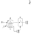
- Figure 1 shows a diagram of an electronic ignition device for an internal combustion engine,
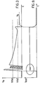
- Figures 2 and 3 show respective diagrams of the electrical signals present in the device in Figure 1 on the same time base,
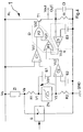
- Figure 4 shows a block diagram of a circuit constructed according to the invention,
- Figure 5 shows a possible application of the circuit constructed according to the invention,
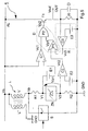
- Figure 6 shows an embodiment of the circuit in the block diagram illustrated in Figure 4,
- Figures 7 and 8 show the change in an output voltage of the circuit according to the invention.
Claims (9)
- A circuit for detecting a time duration of an overvoltage signal (Va) on an electrical load (Z1) inserted with first and second terminals between a feed line (AL) and a control switch (S), said circuit having an output voltage signal (Vout) at an output terminal (OUT) and comprising:at least one first threshold comparator (C1) having a first input terminal receiving a voltage indicative of the overvoltage (Va), said voltage including a first reference voltage (E1) applied to said first input terminal, a second input terminal coupled to the feed line (AL) and an output terminals for producing a first voltage signal (Vc1) at a first logic level when the overvoltage signal (Va) exceeds a second threshold voltage (Vth2) and at a second logic level when the overvoltage signal (Va) falls below a second threshold voltage (Vth2),at least one second threshold comparator (C2) having a first input terminal held at a second reference voltage (E2), a second input terminal receiving a voltage indicative of the overvoltage (Va), and an output terminal for producing a second voltage signal (Vc2) at a first logic level when the overvoltage signal (Va) exceeds a first threshold voltage (Vth1) and at a second logic level when the overvoltage signal (Va) falls below the first threshold voltage (Vth1),at least one output transistor (T1) inserted with first and second terminals between the feed line (AL) and the output terminal (OUT)for producing the output voltage signal (Vout), said transistor (T1) being connected to at least one logic block (D) having inputs connected to the outputs of threshold comparators (C1) and (C2), said logic block (D) being for controlling the output transistor (T1) so as to have the output voltage signal (Vout) at the first logic level when the first (Vc1) and the second (Vc2) voltage signal are at the first logic level,at least one feedback block (R) inserted with an input terminal and an output terminal respectively between the output terminal (OUT) and a further input terminal to the logic block (D), said feedback block (R) being for maintaining the output voltage signal (Vout) at the first logic level for a time interval sufficient to suppress changes in said logic level due to rapid changes of the overvoltage (Va), said time duration being detected by the condition Va<Vth2 persinsting for a sufficient long time in order to distinguish between rapid changes and regular overvoltage duration during the time duration of the overvoltage signal (Va).
- A circuit according to claim 1, characterised in that the feedback block (R) includes at least a third threshold comparator (C3) having a first input terminal held at a third reference voltage (E3), a second input terminal connected to the output (OUT) terminal from circuit (1) and an output terminal.
- A circuit according to claim 1, characterised in that the logic block (D) comprises:at least one first logic gate (P1) having a first input terminal connected to the output terminal of the second threshold comparator (C2), a second input terminal connected to the output terminal from the third threshold comparator (C3) and an output terminal,at least one second logic gate (P2) having a first input terminal connected to the output terminal from the first comparator (C1), a second input terminal connected to the output terminal from the first logic gate (P1) and an output terminal capable of controlling the output transistor (T1).
- A circuit according to claim 1, characterised in that the second input terminal to the second comparator (C2) is connected to the second terminal of the electric load (Z1) through at least one one-way block (ZN) connected in series to a first resistance element (R1).
- A circuit according to claim 1, characterised in that a condenser (C1) connected in parallel to a second resistance element (R1) is inserted between its output terminal (OUT) and a fourth reference voltage (GND).
- A circuit according to claim 3, characterised in that the first logic gate (P1) is of the OR type.
- A circuit according to claim 3, characterised in that the second logic gate (P2) is of the AND type.
- A circuit according to claim 1, characterised in that the output transistor (T1) is of the NPN type.
- A circuit according to claim 1, characterised in that it is integrated using technology of the VIPower type.
Priority Applications (4)
| Application Number | Priority Date | Filing Date | Title |
|---|---|---|---|
| DE69533391T DE69533391D1 (en) | 1995-04-28 | 1995-04-28 | Circuit for detecting an overvoltage on an electrical consumer |
| EP95830168A EP0740073B1 (en) | 1995-04-28 | 1995-04-28 | Circuit for detecting an overvoltage on an electric load |
| JP8105533A JPH08304480A (en) | 1995-04-28 | 1996-04-25 | Overvoltage detector circuit |
| US08/639,794 US5735254A (en) | 1995-04-28 | 1996-04-29 | Circuit for detecting an overvoltage on a switched inductive load |
Applications Claiming Priority (1)
| Application Number | Priority Date | Filing Date | Title |
|---|---|---|---|
| EP95830168A EP0740073B1 (en) | 1995-04-28 | 1995-04-28 | Circuit for detecting an overvoltage on an electric load |
Publications (2)
| Publication Number | Publication Date |
|---|---|
| EP0740073A1 EP0740073A1 (en) | 1996-10-30 |
| EP0740073B1 true EP0740073B1 (en) | 2004-08-18 |
Family
ID=8221907
Family Applications (1)
| Application Number | Title | Priority Date | Filing Date |
|---|---|---|---|
| EP95830168A Expired - Lifetime EP0740073B1 (en) | 1995-04-28 | 1995-04-28 | Circuit for detecting an overvoltage on an electric load |
Country Status (4)
| Country | Link |
|---|---|
| US (1) | US5735254A (en) |
| EP (1) | EP0740073B1 (en) |
| JP (1) | JPH08304480A (en) |
| DE (1) | DE69533391D1 (en) |
Families Citing this family (12)
| Publication number | Priority date | Publication date | Assignee | Title |
|---|---|---|---|---|
| KR100486351B1 (en) * | 1997-11-13 | 2005-07-07 | 페어차일드코리아반도체 주식회사 | Pulse Width Modulation Control with Overload Protection |
| DE60015711T2 (en) | 2000-01-27 | 2005-11-24 | Stmicroelectronics S.R.L., Agrate Brianza | Electronic ignition unit with limitation of the voltage to a connection of the ignition coil primary winding |
| EP1184954A1 (en) * | 2000-08-31 | 2002-03-06 | STMicroelectronics S.r.l. | Integrated and self-supplied voltage regulator and related regulation method |
| JP3607902B2 (en) * | 2002-07-22 | 2005-01-05 | 三菱電機株式会社 | Ignition device for internal combustion engine |
| DE10243858A1 (en) * | 2002-09-20 | 2004-04-01 | Siemens Ag | Power surge protection |
| FR2853941B1 (en) * | 2003-04-17 | 2007-02-09 | Siemens Vdo Automotive | METHOD FOR THE PRIMARY IGNITION CURRENT CHECK OF AN INTERNAL COMBUSTION ENGINE WITH COMMAND IGNITION |
| US8238823B2 (en) * | 2005-02-09 | 2012-08-07 | Nxp B.V. | Method for ensuring a secure NFC functionality of a wireless mobile communication device and wireless mobile communication device having a secure NFC functionality |
| US20100006066A1 (en) * | 2008-07-14 | 2010-01-14 | Nicholas Danne | Variable primary current for ionization |
| US8342151B2 (en) * | 2008-12-18 | 2013-01-01 | GM Global Technology Operations LLC | Deactivation of high pressure pump for noise control |
| CN101557099B (en) * | 2009-05-12 | 2011-09-21 | 中兴通讯股份有限公司 | Module power supply short-circuit protective circuit |
| JP5664327B2 (en) * | 2011-02-23 | 2015-02-04 | 富士電機株式会社 | Control device for DC-DC converter |
| CN105422360B (en) * | 2015-11-30 | 2017-12-15 | 深圳市轱辘车联数据技术有限公司 | A kind of detection circuit of automotive ignition action |
Family Cites Families (14)
| Publication number | Priority date | Publication date | Assignee | Title |
|---|---|---|---|---|
| DE3071012D1 (en) * | 1979-05-25 | 1985-09-26 | Lucas Ind Plc | A test procedure for testing an internal combustion engine electronic ignition system |
| US4380989A (en) * | 1979-11-27 | 1983-04-26 | Nippondenso Co., Ltd. | Ignition system for internal combustion engine |
| US4604750A (en) * | 1983-11-07 | 1986-08-05 | Digital Equipment Corporation | Pipeline error correction |
| US4612640A (en) * | 1984-02-21 | 1986-09-16 | Seeq Technology, Inc. | Error checking and correction circuitry for use with an electrically-programmable and electrically-erasable memory array |
| US4750467A (en) * | 1986-09-11 | 1988-06-14 | General Motors Corporation | Internal combustion engine ignition system |
| JP2606862B2 (en) * | 1987-12-28 | 1997-05-07 | 株式会社東芝 | Single error detection and correction method |
| JP2583547B2 (en) * | 1988-01-13 | 1997-02-19 | 株式会社日立製作所 | Semiconductor memory |
| US4886029A (en) * | 1988-05-26 | 1989-12-12 | Motorola Inc. | Ignition misfire detector |
| US4918389A (en) * | 1988-06-03 | 1990-04-17 | Robert Bosch Gmbh | Detecting misfiring in spark ignition engines |
| JP2664236B2 (en) * | 1989-02-01 | 1997-10-15 | 富士通株式会社 | Semiconductor storage device |
| DE3907616A1 (en) * | 1989-03-09 | 1990-09-20 | Bosch Gmbh Robert | CIRCUIT ARRANGEMENT FOR MEASURING THE PRIMARY VOLTAGE OF A IGNITION COIL |
| DE4107335A1 (en) * | 1991-03-07 | 1992-09-10 | Beru Werk Ruprecht Gmbh Co A | METHOD AND DEVICE FOR MONITORING A IGNITION SYSTEM |
| US5309888A (en) * | 1991-08-02 | 1994-05-10 | Motorola, Inc. | Ignition system |
| US5446385A (en) * | 1992-10-02 | 1995-08-29 | Robert Bosch Gmbh | Ignition system for internal combustion engines |
-
1995
- 1995-04-28 DE DE69533391T patent/DE69533391D1/en not_active Expired - Lifetime
- 1995-04-28 EP EP95830168A patent/EP0740073B1/en not_active Expired - Lifetime
-
1996
- 1996-04-25 JP JP8105533A patent/JPH08304480A/en active Pending
- 1996-04-29 US US08/639,794 patent/US5735254A/en not_active Expired - Lifetime
Also Published As
| Publication number | Publication date |
|---|---|
| JPH08304480A (en) | 1996-11-22 |
| EP0740073A1 (en) | 1996-10-30 |
| US5735254A (en) | 1998-04-07 |
| DE69533391D1 (en) | 2004-09-23 |
Similar Documents
| Publication | Publication Date | Title |
|---|---|---|
| EP0740073B1 (en) | Circuit for detecting an overvoltage on an electric load | |
| EP0366622A2 (en) | A circuit for piloting an inductive load, particularly for controlling the electro-injectors of a diesel engine | |
| US20010040470A1 (en) | Method and device for driving a power output stage | |
| US4520420A (en) | Current control method and apparatus for electromagnetic valves | |
| US7525783B2 (en) | Monitoring method for an actuator and corresponding driver circuit | |
| US6060814A (en) | Device and method for driving at least one capacitive actuator | |
| EP0763882A1 (en) | Load driving device | |
| US4314305A (en) | Solenoid drive circuits | |
| US6456156B1 (en) | Method and device for the open-load diagnosis of a switching stage | |
| US6531908B1 (en) | Power output stage for switching inductive loads with reduced radiation emission | |
| EP0924589A1 (en) | Electroactuator control device and method for controlling this control device | |
| US5218339A (en) | Arrangement for monitoring a consumer in combination with an internal combustion engine and/or a motor vehicle | |
| US4246881A (en) | System for decreasing the power consumption in the output transistor of an ignition system | |
| US20020144544A1 (en) | Automotive ignition monitoring system with misfire and fouled plug detection | |
| US7367302B2 (en) | Method and device for switching on a power switch arranged between capacitive elements | |
| US4461979A (en) | Low-drive power switching transistor control circuit | |
| EP0590223B1 (en) | Method and device to recover energy in driving inductive loads | |
| JP2000110640A (en) | Solenoid valve driving device | |
| US4097770A (en) | SCR trigger circuit | |
| WO1998026487A1 (en) | Device including a thermally protected switching transistor | |
| US4105006A (en) | Ignition system for internal combustion engine | |
| US4448180A (en) | Ignition system for an internal combustion engine | |
| JP3801336B2 (en) | Load drive device | |
| JP3843332B2 (en) | Electromagnetic actuator drive | |
| US6194951B1 (en) | Method and device for diving an integrated power output stage |
Legal Events
| Date | Code | Title | Description |
|---|---|---|---|
| PUAI | Public reference made under article 153(3) epc to a published international application that has entered the european phase |
Free format text: ORIGINAL CODE: 0009012 |
|
| AK | Designated contracting states |
Kind code of ref document: A1 Designated state(s): DE FR GB IT |
|
| 17P | Request for examination filed |
Effective date: 19970421 |
|
| 17Q | First examination report despatched |
Effective date: 19970924 |
|
| RAP3 | Party data changed (applicant data changed or rights of an application transferred) |
Owner name: STMICROELECTRONICS S.R.L. Owner name: CO.RI.M.ME. CONSORZIO PER LA RICERCA SULLA MICROEL |
|
| GRAP | Despatch of communication of intention to grant a patent |
Free format text: ORIGINAL CODE: EPIDOSNIGR1 |
|
| GRAS | Grant fee paid |
Free format text: ORIGINAL CODE: EPIDOSNIGR3 |
|
| GRAA | (expected) grant |
Free format text: ORIGINAL CODE: 0009210 |
|
| AK | Designated contracting states |
Kind code of ref document: B1 Designated state(s): DE FR GB IT |
|
| PG25 | Lapsed in a contracting state [announced via postgrant information from national office to epo] |
Ref country code: FR Free format text: LAPSE BECAUSE OF FAILURE TO SUBMIT A TRANSLATION OF THE DESCRIPTION OR TO PAY THE FEE WITHIN THE PRESCRIBED TIME-LIMIT Effective date: 20040818 |
|
| REG | Reference to a national code |
Ref country code: GB Ref legal event code: FG4D |
|
| REF | Corresponds to: |
Ref document number: 69533391 Country of ref document: DE Date of ref document: 20040923 Kind code of ref document: P |
|
| PG25 | Lapsed in a contracting state [announced via postgrant information from national office to epo] |
Ref country code: DE Free format text: LAPSE BECAUSE OF FAILURE TO SUBMIT A TRANSLATION OF THE DESCRIPTION OR TO PAY THE FEE WITHIN THE PRESCRIBED TIME-LIMIT Effective date: 20041119 |
|
| PG25 | Lapsed in a contracting state [announced via postgrant information from national office to epo] |
Ref country code: IT Free format text: LAPSE BECAUSE OF NON-PAYMENT OF DUE FEES;WARNING: LAPSES OF ITALIAN PATENTS WITH EFFECTIVE DATE BEFORE 2007 MAY HAVE OCCURRED AT ANY TIME BEFORE 2007. THE CORRECT EFFECTIVE DATE MAY BE DIFFERENT FROM THE ONE RECORDED. Effective date: 20050428 |
|
| PLBE | No opposition filed within time limit |
Free format text: ORIGINAL CODE: 0009261 |
|
| STAA | Information on the status of an ep patent application or granted ep patent |
Free format text: STATUS: NO OPPOSITION FILED WITHIN TIME LIMIT |
|
| 26N | No opposition filed |
Effective date: 20050519 |
|
| EN | Fr: translation not filed | ||
| PGFP | Annual fee paid to national office [announced via postgrant information from national office to epo] |
Ref country code: GB Payment date: 20070328 Year of fee payment: 13 |
|
| GBPC | Gb: european patent ceased through non-payment of renewal fee |
Effective date: 20080428 |
|
| PG25 | Lapsed in a contracting state [announced via postgrant information from national office to epo] |
Ref country code: GB Free format text: LAPSE BECAUSE OF NON-PAYMENT OF DUE FEES Effective date: 20080428 |