EP0736907B1 - Semiconductor field effect device with an integrated ohmic resistance - Google Patents
Semiconductor field effect device with an integrated ohmic resistance Download PDFInfo
- Publication number
- EP0736907B1 EP0736907B1 EP96104243A EP96104243A EP0736907B1 EP 0736907 B1 EP0736907 B1 EP 0736907B1 EP 96104243 A EP96104243 A EP 96104243A EP 96104243 A EP96104243 A EP 96104243A EP 0736907 B1 EP0736907 B1 EP 0736907B1
- Authority
- EP
- European Patent Office
- Prior art keywords
- contact area
- gate electrode
- gate
- reactive resistor
- contact
- Prior art date
- Legal status (The legal status is an assumption and is not a legal conclusion. Google has not performed a legal analysis and makes no representation as to the accuracy of the status listed.)
- Expired - Lifetime
Links
- 239000004065 semiconductor Substances 0.000 title claims description 23
- 230000005669 field effect Effects 0.000 title description 6
- 229910021420 polycrystalline silicon Inorganic materials 0.000 claims description 22
- 229920005591 polysilicon Polymers 0.000 claims description 19
- 239000002184 metal Substances 0.000 claims description 6
- 239000004020 conductor Substances 0.000 description 3
- 238000001465 metallisation Methods 0.000 description 2
- 230000007423 decrease Effects 0.000 description 1
- 230000001419 dependent effect Effects 0.000 description 1
- 238000011161 development Methods 0.000 description 1
- 230000018109 developmental process Effects 0.000 description 1
- 230000000694 effects Effects 0.000 description 1
- 238000005530 etching Methods 0.000 description 1
- 238000005468 ion implantation Methods 0.000 description 1
- 230000003071 parasitic effect Effects 0.000 description 1
- 238000004513 sizing Methods 0.000 description 1
Images

Classifications
-
- H—ELECTRICITY
- H01—ELECTRIC ELEMENTS
- H01L—SEMICONDUCTOR DEVICES NOT COVERED BY CLASS H10
- H01L29/00—Semiconductor devices specially adapted for rectifying, amplifying, oscillating or switching and having potential barriers; Capacitors or resistors having potential barriers, e.g. a PN-junction depletion layer or carrier concentration layer; Details of semiconductor bodies or of electrodes thereof ; Multistep manufacturing processes therefor
- H01L29/40—Electrodes ; Multistep manufacturing processes therefor
- H01L29/41—Electrodes ; Multistep manufacturing processes therefor characterised by their shape, relative sizes or dispositions
- H01L29/423—Electrodes ; Multistep manufacturing processes therefor characterised by their shape, relative sizes or dispositions not carrying the current to be rectified, amplified or switched
- H01L29/42312—Gate electrodes for field effect devices
- H01L29/42316—Gate electrodes for field effect devices for field-effect transistors
- H01L29/4232—Gate electrodes for field effect devices for field-effect transistors with insulated gate
- H01L29/42372—Gate electrodes for field effect devices for field-effect transistors with insulated gate characterised by the conducting layer, e.g. the length, the sectional shape or the lay-out
- H01L29/4238—Gate electrodes for field effect devices for field-effect transistors with insulated gate characterised by the conducting layer, e.g. the length, the sectional shape or the lay-out characterised by the surface lay-out
-
- H—ELECTRICITY
- H01—ELECTRIC ELEMENTS
- H01L—SEMICONDUCTOR DEVICES NOT COVERED BY CLASS H10
- H01L29/00—Semiconductor devices specially adapted for rectifying, amplifying, oscillating or switching and having potential barriers; Capacitors or resistors having potential barriers, e.g. a PN-junction depletion layer or carrier concentration layer; Details of semiconductor bodies or of electrodes thereof ; Multistep manufacturing processes therefor
- H01L29/66—Types of semiconductor device ; Multistep manufacturing processes therefor
- H01L29/68—Types of semiconductor device ; Multistep manufacturing processes therefor controllable by only the electric current supplied, or only the electric potential applied, to an electrode which does not carry the current to be rectified, amplified or switched
- H01L29/76—Unipolar devices, e.g. field effect transistors
-
- H—ELECTRICITY
- H01—ELECTRIC ELEMENTS
- H01L—SEMICONDUCTOR DEVICES NOT COVERED BY CLASS H10
- H01L29/00—Semiconductor devices specially adapted for rectifying, amplifying, oscillating or switching and having potential barriers; Capacitors or resistors having potential barriers, e.g. a PN-junction depletion layer or carrier concentration layer; Details of semiconductor bodies or of electrodes thereof ; Multistep manufacturing processes therefor
- H01L29/40—Electrodes ; Multistep manufacturing processes therefor
- H01L29/43—Electrodes ; Multistep manufacturing processes therefor characterised by the materials of which they are formed
- H01L29/435—Resistive materials for field effect devices, e.g. resistive gate for MOSFET or MESFET
-
- H—ELECTRICITY
- H01—ELECTRIC ELEMENTS
- H01L—SEMICONDUCTOR DEVICES NOT COVERED BY CLASS H10
- H01L2224/00—Indexing scheme for arrangements for connecting or disconnecting semiconductor or solid-state bodies and methods related thereto as covered by H01L24/00
- H01L2224/01—Means for bonding being attached to, or being formed on, the surface to be connected, e.g. chip-to-package, die-attach, "first-level" interconnects; Manufacturing methods related thereto
- H01L2224/42—Wire connectors; Manufacturing methods related thereto
- H01L2224/47—Structure, shape, material or disposition of the wire connectors after the connecting process
- H01L2224/48—Structure, shape, material or disposition of the wire connectors after the connecting process of an individual wire connector
- H01L2224/484—Connecting portions
- H01L2224/4847—Connecting portions the connecting portion on the bonding area of the semiconductor or solid-state body being a wedge bond
-
- H—ELECTRICITY
- H01—ELECTRIC ELEMENTS
- H01L—SEMICONDUCTOR DEVICES NOT COVERED BY CLASS H10
- H01L2924/00—Indexing scheme for arrangements or methods for connecting or disconnecting semiconductor or solid-state bodies as covered by H01L24/00
- H01L2924/10—Details of semiconductor or other solid state devices to be connected
- H01L2924/11—Device type
- H01L2924/13—Discrete devices, e.g. 3 terminal devices
- H01L2924/1304—Transistor
- H01L2924/1305—Bipolar Junction Transistor [BJT]
- H01L2924/13055—Insulated gate bipolar transistor [IGBT]
-
- H—ELECTRICITY
- H01—ELECTRIC ELEMENTS
- H01L—SEMICONDUCTOR DEVICES NOT COVERED BY CLASS H10
- H01L2924/00—Indexing scheme for arrangements or methods for connecting or disconnecting semiconductor or solid-state bodies as covered by H01L24/00
- H01L2924/10—Details of semiconductor or other solid state devices to be connected
- H01L2924/11—Device type
- H01L2924/13—Discrete devices, e.g. 3 terminal devices
- H01L2924/1304—Transistor
- H01L2924/1306—Field-effect transistor [FET]
- H01L2924/13091—Metal-Oxide-Semiconductor Field-Effect Transistor [MOSFET]
Definitions
- the invention relates to a controllable by field effect Semiconductor component with a semiconductor body on which one isolated from the surface of the semiconductor body doped polysilicon layer is arranged, one of which first part is a gate electrode and a second part is one Contact area for a gate lead.
- Semiconductor components of the aforementioned that can be controlled by field effect Type e.g. Power MOSFET or IGBT are state of the art Technology. E.g. there are generally many such in modules Semiconductor components connected in parallel. Because of of the parasitic line inductances in the control circuit tend such arrangements when leading control to vibrations that prevent a defined switching on.
- a power MOS transistor is described in US Pat. No. 4,920,388. which contains a polycrystalline silicon layer, the as a resistance between a gate metallization and the gate terminal of the power MOS transistor is used. Furthermore, the semiconductor component contains a second one Area of a gate metallization that is adjacent to the active The source gate region of the component lies.
- JP-A-05055588 is a multi-chip-like MOS field effect transistor described a resistance with a higher Has impedance as a bond wire, and that between the Gate electrode and the gate contact area lies.
- the resistance is in by a lightly doped polysilicon layer a predetermined area.
- JP-A-62098670 is a semiconductor device with one with the gate connected in series resistance, arranged between the gate pad and the gate is.
- the resistor is made of polysilicon and its resistance value can be adjusted by ion implantation.
- the invention has for its object a field effect controllable semiconductor device of the type described to develop such that a simple and inexpensive Manufacturability is possible. Furthermore, the contact area easy and safe to contact for a gate lead be.
- the contact surface on Edge is provided with at least one recess, the ohmic resistance is arranged in the recess.
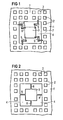
- Figure 1 is a section of a controllable by field effect Semiconductor device shown.
- the surface of a semiconductor body is covered with an insulating layer (not shown), on which in turn a doped polysilicon layer is arranged.
- the polysilicon layer has one first part 1, which serves as a gate electrode and a second Part 3, which is the contact surface for attaching a Gate lead forms.
- the gate electrode 1 of the polysilicon layer is provided with openings 2 through which -insulated against the polysilicon layer - via contact holes Source zones of the individual cells of the semiconductor component are contacted. These contact holes form a regular, distributed over the surface of the gate electrode 1 Template. To accommodate so-called gate contact fingers better distribution of the gate potential with larger chips can open wider areas 7 between adjacent cells of contact holes.
- the gate electrode 1 has a recess 4 in which the contact area 3 is arranged. Between the contact surface 3 and the gate electrode 1 is the doped polysilicon e.g. by Etching interrupted. In the recess 4 are between the Contact surface 3 and the gate electrode 1 islands 5, the integrated form ohmic resistors. They preferably exist made of doped polycrystalline silicon and have the same Doping like the contact area 3 and the gate electrode 1. They preferably also have the same thickness as 1 and 3.
- the islands 5 are on the one hand via conductor tracks 6 with the Gate electrode 1 and on the other hand with the contact surface 3 connected.
- the islands 5 can be generated simultaneously with the structuring of the contact area 3 and the gate electrode 1. Their length and cross-section depend on the size of the gate series resistor R g .
- the contact surface 3 is connected to the gate electrode 1 by means of webs 8.
- webs 8. are. These also consist of polysilicon. Their length and their cross section in turn depend on the resistance value that the gate series resistor R g should have.
- the embodiment of Figure 3 differs from that of Figure 1 in that the islands 5 in recesses 24th a contact surface 23 are arranged.
- the islands become 5 here as in the embodiment of Figure 1 by conductor tracks on the one hand with the contact surface 23 and on the other hand with contacted the gate electrode 1.
- the recesses 24 can as shown at the corners of the contact surface 23 or also in other places of the scope.
- the islands 5 can like the cutouts are square, other shapes are possible.
- Figure 4 it is shown that the surface of a semiconductor device with the semiconductor zones 11, 14 with a Oxide layer 12 is covered. This lies on the oxide layer 12 structured polysilicon layer consisting of the contact area 3, the islands 5 and the gate electrode 1.
- On the Polysilicon layer is an insulating layer 10 that both the gate electrode 1 and the contact surface 3 and Islands 5 covered.
- On the oxide layer 10 is above the Contact surface 3, a metal layer 14 is arranged.
- On the Gate electrode 1 sits a mentioned in connection with Figure 1 Gate contact finger 15. It is also through a metal layer educated.
- the metal layer 14 is on the contact surface 3 via contact holes 19 with the underlying polysilicon layer electrically connected. In the same way it is Gate contact finger 15 via contact holes 16 with the gate electrode 1 connected.
- the separate conductor tracks 6 are via contact holes 17 with the island's 5 polysilicon, which is the resistor represents connected.
- the metal layer 14 protrudes a bond wire 18 with an external connection of the semiconductor component in connection.
- the islands 5 or the webs 8 are according to one Embodiment by 0.5 to 1 micron thick polysilicon educated. Their width and length can e.g. 0.5 mm be.
- the polysilicon can e.g. be endowed in such a way that it has a resistance of 20 ohms / ⁇ .
Landscapes
- Engineering & Computer Science (AREA)
- Microelectronics & Electronic Packaging (AREA)
- Power Engineering (AREA)
- Physics & Mathematics (AREA)
- Ceramic Engineering (AREA)
- Condensed Matter Physics & Semiconductors (AREA)
- General Physics & Mathematics (AREA)
- Computer Hardware Design (AREA)
- Semiconductor Integrated Circuits (AREA)
- Insulated Gate Type Field-Effect Transistor (AREA)
- Electrodes Of Semiconductors (AREA)
Description
Die Erfindung bezieht sich auf ein durch Feldeffekt steuerbares Halbleiterbauelement mit einem Halbleiterkörper, auf dem eine gegen die Oberfläche des Halbleiterkörpers isolierte dotierte Polysiliziumschicht angeordnet ist, von der ein erster Teil eine Gateelektrode ist und ein zweiter Teil eine Kontaktfläche für eine Gatezuleitung.The invention relates to a controllable by field effect Semiconductor component with a semiconductor body on which one isolated from the surface of the semiconductor body doped polysilicon layer is arranged, one of which first part is a gate electrode and a second part is one Contact area for a gate lead.
Durch Feldeffekt steuerbare Halbleiterbauelemente der erwähnten Art, z.B. Leistungs-MOSFET oder IGBT, sind Stand der Technik. Z.B. in Modulen werden im allgemeinen viele solcher Halbleiterbauelemente einander parallel geschaltet. Aufgrund der parasitären Leitungsinduktivitäten im Steuerkreis neigen solche Anordnungen beim Leitendsteuern zu Schwingungen, die ein definiertes Einschalten verhindern.Semiconductor components of the aforementioned that can be controlled by field effect Type, e.g. Power MOSFET or IGBT are state of the art Technology. E.g. there are generally many such in modules Semiconductor components connected in parallel. Because of of the parasitic line inductances in the control circuit tend such arrangements when leading control to vibrations that prevent a defined switching on.
Bisher wurden daher in die Module Widerstandschips eingebaut, die einerseits mit den Gatenanschlüssen der Halbleiterbauelemente und andererseits mit externen Gateanschlüssen des Moduls durch Bonddrähte verbunden werden müssen. Diese Lösung erfordert zusätzliche Fläche im Modul und zusätzliche Verbindungsleitungen.So far, resistance chips have been built into the modules, on the one hand with the gate connections of the semiconductor components and on the other hand with external gate connections of the Module must be connected by bond wires. This solution requires additional space in the module and additional connecting cables.
In der US 4,920,388 ist ein Leistungs-MOS-Transistor beschrieben, der eine polykristalline Siliziumschicht beinhaltet, die als Widerstand zwischen einer Gate-Metallisierung und dem Gateanschluß des Leistungs-MOS-Transistors dient. Weiterhin beinhaltet das Halbleiterbauelement einen zweiten Bereich einer Gate-Metallisierung, die benachbart der aktiven Source-Gate-Region des Bauelementes liegt.A power MOS transistor is described in US Pat. No. 4,920,388. which contains a polycrystalline silicon layer, the as a resistance between a gate metallization and the gate terminal of the power MOS transistor is used. Furthermore, the semiconductor component contains a second one Area of a gate metallization that is adjacent to the active The source gate region of the component lies.
In Patent Abstracts of Japan, Vol. 017, No. 356, 6. Juli 1993 + JP-A-05055588 ist ein Multi-Chip-ähnlicher MOS-Feldeffekt-transistor beschrieben, der einen Widerstand mit einer höheren Impedanz aufweist als ein Bonddraht, und der zwischen der Gate-Elektrode und der Gate-Kontaktfläche liegt. Der Widerstand ist durch eine leicht dotierte Polysiliziumschicht in einem vorgegebenen Bereich gebildet.In Patent Abstracts of Japan, Vol. 017, No. 356, July 6, 1993 + JP-A-05055588 is a multi-chip-like MOS field effect transistor described a resistance with a higher Has impedance as a bond wire, and that between the Gate electrode and the gate contact area lies. The resistance is in by a lightly doped polysilicon layer a predetermined area.
In Patent Abstracts of Japan, Vol. 011, No. 306, 6. Oktober 1987 + JP-A-62098670 ist ein Halbleiterbauelement mit einem mit dem Gate in Serie geschaltenen Widerstand beschrieben, der zwischen der Gate-Kontaktfläche und dem Gate angeordnet ist. Der Widerstand besteht aus Polysilizium und sein Widerstandswert kann durch Ionenimplantation eingestellt werden.In Patent Abstracts of Japan, Vol. 011, No. 306, October 6 1987 + JP-A-62098670 is a semiconductor device with one with the gate connected in series resistance, arranged between the gate pad and the gate is. The resistor is made of polysilicon and its resistance value can be adjusted by ion implantation.
In dem Artikel "A Study on the Effect of the Gate Contact Geometry and Dimensions on ESD Failure Threshold Level of Power MOSFET's", K. Throngnumchai, IEEE Transactions on Electron Devices, July 1994, USA, Vol. 41, No. 7, Pages 1282 - 1287 ist beschrieben, wie durch Ausgestaltung der Gate-Kontaktelektrode und über Dimensionierung Fehler des Leistungs-MOSFETs durch elektrostatische Entladung (ESD) vermieden werden können. Zu diesem Zweck sollte die Gate-Kontaktelektrode in ihrer Breite vergrößert werden sowie der aus Polysilizium bestehende Widerstand zwischen dem Gateanschluß und der Kontaktelektrode verringert werden.In the article "A Study on the Effect of the Gate Contact Geometry and Dimensions on ESD Failure Threshold Level of Power MOSFETs ", K. Throngnumchai, IEEE Transactions on Electron Devices, July 1994, USA, Vol. 41, No. 7, Pages 1282 - 1287 is described as by designing the gate contact electrode and about sizing errors of the Power MOSFETs through electrostatic discharge (ESD) can be avoided. For this purpose, the gate contact electrode be enlarged in width as well as the Resistor made of polysilicon between the gate connection and the contact electrode can be reduced.
Der Erfindung liegt die Aufgabe zugrunde, ein durch Feldeffekt steuerbares Halbleiterbauelement der beschriebenen Art derart weiterzubilden, daß eine einfache und kostengünstige Herstellbarkeit möglich ist. Ferner soll die Kontaktfläche für eine Gatezuleitung einfach und sicher zu kontaktieren sein.The invention has for its object a field effect controllable semiconductor device of the type described to develop such that a simple and inexpensive Manufacturability is possible. Furthermore, the contact area easy and safe to contact for a gate lead be.
Diese Aufgabe wird dadurch gelöst, daß die Kontaktfläche am Rand mit mindestens einer Aussparung versehen ist, wobei der ohmsche Widerstand in der Aussparung angeordnet ist. This object is achieved in that the contact surface on Edge is provided with at least one recess, the ohmic resistance is arranged in the recess.
Weiterbildungen der Erfindung sind Gegenstand der Unteransprüche.Developments of the invention are the subject of the dependent claims.
Die Erfindung wird anhand einiger Ausführungsbeispiele in Verbindung mit den Figuren 1 bis 4 näher erläutert. Es zeigen
Figuren 1 bis 3- die Aufsicht auf je ein Ausführungsbeispiel und
Figur 4- einen Schnitt durch ein weiteres Ausführungsbeispiel.
- Figures 1 to 3
- supervision of one embodiment and
- Figure 4
- a section through a further embodiment.
In Figur 1 ist ein Ausschnitt eines durch Feldeffekt steuerbaren
Halbleiterbauelementes dargestellt. Die Oberfläche
eines Halbleiterkörpers ist mit einer Isolierschicht bedeckt
(nicht dargestellt), auf der wiederum eine dotierte Polysiliziumschicht
angeordnet ist. Die Polysiliziumschicht hat einen
ersten Teil 1, der als Gateelektrode dient und einen zweiten
Teil 3, der die Kontaktfläche für die Befestigung einer
Gatezuleitung bildet. Die Gateelektrode 1 der Polysiliziumschicht
ist mit Öffnungen 2 versehen, durch die -isoliert
gegen die Polysiliziumschicht- über Kontakt löcher die
Sourcezonen der einzelnen Zellen des Halbleiterbauelementes
kontaktiert sind. Diese Kontaktlöcher bilden ein regelmäßiges,
über die Oberfläche der Gateelektrode 1 verteiltes
Muster. Zur Aufnahme von sogenannten Gatekontaktfingern zur
besseren Verteilung des Gatepotentials bei größeren Chips
können zwischen benachbarten Zellen breitere Flächen 7 frei
von Kontaktlöchern sein.In Figure 1 is a section of a controllable by field effect
Semiconductor device shown. The surface
of a semiconductor body is covered with an insulating layer
(not shown), on which in turn a doped polysilicon layer
is arranged. The polysilicon layer has one
Die Gateelektrode 1 hat eine Aussparung 4, in der die Kontaktfläche
3 angeordnet ist. Zwischen der Kontaktfläche 3 und
der Gateelektrode 1 ist das dotierte Polysilizium z.B. durch
Ätzen unterbrochen. In der Aussparung 4 liegen zwischen der
Kontaktfläche 3 und der Gateelektrode 1 Inseln 5, die integrierte
ohmsche Widerstände bilden. Sie bestehen vorzugsweise
aus dotiertem polykristallinem Silizium und haben die gleiche
Dotierung wie die Kontaktfläche 3 und die Gateelektrode 1.
Sie haben vorzugsweise auch die gleiche Dicke wie 1 und 3. The
Die Inseln 5 sind über Leiterbahnen 6 einerseits mit der
Gateelektrode 1 und andererseits mit der Kontaktfläche 3
verbunden.The
Die Inseln 5 können gleichzeitig mit der Strukturierung der
Kontaktfläche 3 und der Gateelektrode 1 erzeugt werden. Ihre
Länge und ihr Querschnitt richten sich danach, welche Größe
der Gatevorwiderstand Rg haben soll.The
Im Ausführungsbeispiel nach Figur 2 ist die Kontaktfläche 3
mit der Gateelektrode 1 durch Stege 8 verbunden. ist. Diese
bestehen ebenfalls aus Polysilizium. Ihre Länge und ihr
Querschnitt richten sich wiederum nach demjenigen Widerstandswert,
den der Gatevorwiderstand Rg haben soll.In the exemplary embodiment according to FIG. 2, the
Das Ausführungsbeispiel nach Figur 3 unterscheidet sich von
dem der Figur 1 dadurch, daß die Inseln 5 in Aussparungen 24
einer Kontaktfläche 23 angeordnet sind. Die Inseln 5 werden
hier wie im Ausführungsbeispiel nach Figur 1 durch Leiterbahnen
einerseits mit der Kontaktfläche 23 und andererseits mit
der Gateelektrode 1 kontaktiert. Die Aussparungen 24 können
wie dargestellt an den Ecken der Kontaktfläche 23 liegen oder
auch an anderen Stellen des Umfangs. Die Inseln 5 können wie
die Aussparungen quadratisch sein, andere Formen sind möglich.The embodiment of Figure 3 differs from
that of Figure 1 in that the
In Figur 4 ist dargestellt, daß die Oberfläche eines Halbleiterbauelementes
mit den Halbleiterzonen 11, 14 mit einer
Oxidschicht 12 bedeckt ist. Auf der Oxidschicht 12 liegt die
strukturierte Polysiliziumschicht bestehend aus der Kontaktfläche
3, den Inseln 5 und der Gateelektrode 1. Auf der
Polysiliziumschicht liegt eine Isolierschicht 10, die sowohl
die Gateelektrode 1 als auch die Kontaktfläche 3 und die
Inseln 5 bedeckt. Auf der Oxidschicht 10 ist oberhalb der
Kontaktfläche 3 eine Metallschicht 14 angeordnet. Auf der
Gateelektrode 1 sitzt ein in Verbindung mit Figur 1 erwähnter
Gatekontaktfinger 15. Auch er ist durch eine Metallschicht
gebildet. Die Metallschicht 14 auf der Kontaktfläche 3 ist
über Kontakt löcher 19 mit der darunter liegenden Polysiliziumschicht
elektrisch verbunden. Auf gleiche Weise ist der
Gatekontaktfinger 15 über Kontakt löcher 16 mit der Gatelektrode
1 verbunden. Da auch die Insel 5 mit der Oxidschicht 10
bedeckt ist, sind die getrennten Leiterbahnen 6 über Kontaktlöcher
17 mit dem Polysilizium der Insel 5, die den Widerstand
darstellt, verbunden. Die Metallschicht 14 steht über
einen Bonddraht 18 mit einem externen Anschluß des Halbleiterbauelements
in Verbindung.In Figure 4 it is shown that the surface of a semiconductor device
with the
Die Inseln 5 bzw. die Stege 8 (Figur 2) werden gemäß einem
Ausführungsbeispiel durch 0,5 bis 1 µm dickes Polysilizium
gebildet. Ihre Breite und ihre Länge können z.B. 0,5 mm
betragen. Das Polysilizium kann z.B. derart dotiert sein, daß
es einen Widerstand von 20 Ohm/□ hat.The
Beim Schnitt nach Figur 4 wurde vereinfachend nur eine einzige
Widerstandsinsel 5 dargestellt. Es können jedoch wie in
den Figuren 1, 2 und 3 auch mehrere Widerstände integriert
werden. Entsprechend der Anzahl der parallelgeschalteten
Widerstände verringert sich dann der Widerstandswert für Rg.In the section according to FIG. 4, only a
Claims (5)
- Field effect-controllable semiconductor component having a semiconductor body on which is arranged a doped polysilicon layer which is insulated from the surface of the semiconductor body, a first part of which polysilicon layer is a gate electrode (1) and a second part of which polysilicon layer is a contact area (3) for a gate supply lead, in which the contact area is electrically connected to the gate electrode via at least one integrated non-reactive resistor situated between the contact area (3) and the gate electrode (1), the non-reactive resistor being composed of doped polycrystalline silicon,
characterized in that the contact area (23) is provided with at least one cutout (24) at the edge, and in that the non-reactive resistor (5) is arranged in the cutout. - Semiconductor component according to Claim 1,
characterized in that the non-reactive resistor is connected to the contact area (3) via at least one interconnect (6) and is connected to the gate electrode (1) via at least one interconnect (6). - Semiconductor component according to Claim 1,
characterized in that the contact area (3) is designed to be rectangular, and in that a non-reactive resistor (5) is arranged at or in the vicinity of each corner. - Semiconductor component according to Claim 3,
characterized in that each corner of the contact area has a square cutout (24), and in that a square non-reactive resistor (5) is arranged in each cutout. - Semiconductor component according to Claim 1 or 2,
characterized in that the contact area (3), the non-reactive resistor (5) and the gate electrode (1) are covered with an insulating layer (10), in that a respective metal layer (14, 15) lies on the insulating layer above the gate electrode and above the contact area, which metal layers are electrically connected respectively to the gate electrode and to the contact area via contact holes (16, 19) provided in the insulating layer, and in that the interconnects (6) are electrically connected to the non-reactive resistor (5), to the contact area (3) and to the gate electrode (1) likewise via contact holes (17).
Applications Claiming Priority (2)
| Application Number | Priority Date | Filing Date | Title |
|---|---|---|---|
| DE19512799A DE19512799C2 (en) | 1995-04-05 | 1995-04-05 | Semiconductor component controllable by field effect |
| DE19512799 | 1995-04-05 |
Publications (2)
| Publication Number | Publication Date |
|---|---|
| EP0736907A1 EP0736907A1 (en) | 1996-10-09 |
| EP0736907B1 true EP0736907B1 (en) | 1999-12-22 |
Family
ID=7758878
Family Applications (1)
| Application Number | Title | Priority Date | Filing Date |
|---|---|---|---|
| EP96104243A Expired - Lifetime EP0736907B1 (en) | 1995-04-05 | 1996-03-18 | Semiconductor field effect device with an integrated ohmic resistance |
Country Status (5)
| Country | Link |
|---|---|
| US (1) | US5726474A (en) |
| EP (1) | EP0736907B1 (en) |
| JP (1) | JP3677346B2 (en) |
| KR (1) | KR100397079B1 (en) |
| DE (2) | DE19512799C2 (en) |
Families Citing this family (15)
| Publication number | Priority date | Publication date | Assignee | Title |
|---|---|---|---|---|
| US6069398A (en) * | 1997-08-01 | 2000-05-30 | Advanced Micro Devices, Inc. | Thin film resistor and fabrication method thereof |
| JP2002505525A (en) | 1998-02-27 | 2002-02-19 | アーベーベー (シュヴァイツ) アクチェンゲゼルシャフト | Insulated gate bipolar transistor |
| DE19808154A1 (en) * | 1998-02-27 | 1999-09-02 | Asea Brown Boveri | Bipolar transistor with insulated gate (IGBT) |
| DE19823170A1 (en) * | 1998-05-23 | 1999-11-25 | Asea Brown Boveri | Bipolar transistor with insulated gate electrode |
| JP2994326B2 (en) * | 1998-04-27 | 1999-12-27 | 日本電気アイシーマイコンシステム株式会社 | Semiconductor device |
| US6992916B2 (en) * | 2003-06-13 | 2006-01-31 | Taiwan Semiconductor Manufacturing Co., Ltd. | SRAM cell design with high resistor CMOS gate structure for soft error rate improvement |
| US7486541B2 (en) * | 2003-06-13 | 2009-02-03 | Taiwan Semiconductor Manufacturing Company, Ltd. | Resistive cell structure for reducing soft error rate |
| US8155916B2 (en) | 2008-07-07 | 2012-04-10 | Infineon Technologies Ag | Semiconductor component and method of determining temperature |
| US8314462B2 (en) | 2009-07-28 | 2012-11-20 | Cree, Inc. | Semiconductor devices including electrodes with integrated resistances |
| EP2602828A1 (en) | 2011-12-07 | 2013-06-12 | Nxp B.V. | Semiconductor device having isolation trenches |
| US9917102B2 (en) | 2013-11-28 | 2018-03-13 | Rohm Co., Ltd. | Semiconductor device |
| DE102017105548A1 (en) | 2017-03-15 | 2018-09-20 | Infineon Technologies Dresden Gmbh | SEMICONDUCTOR DEVICE CONTAINING A GATE CONTACT STRUCTURE |
| JP7127413B2 (en) * | 2018-08-03 | 2022-08-30 | 富士電機株式会社 | Resistance element and its manufacturing method |
| JP7180359B2 (en) * | 2018-12-19 | 2022-11-30 | 富士電機株式会社 | resistive element |
| US11664436B2 (en) * | 2021-03-01 | 2023-05-30 | Wolfspeed, Inc. | Semiconductor devices having gate resistors with low variation in resistance values |
Family Cites Families (7)
| Publication number | Priority date | Publication date | Assignee | Title |
|---|---|---|---|---|
| JPS60171771A (en) * | 1984-02-17 | 1985-09-05 | Hitachi Ltd | Insulated gate semiconductor device |
| JPH0758781B2 (en) * | 1985-10-24 | 1995-06-21 | 三菱電機株式会社 | Field effect semiconductor device |
| US4920388A (en) * | 1987-02-17 | 1990-04-24 | Siliconix Incorporated | Power transistor with integrated gate resistor |
| US5182225A (en) * | 1990-01-10 | 1993-01-26 | Microunity Systems Engineering, Inc. | Process for fabricating BICMOS with hypershallow junctions |
| JPH03238868A (en) * | 1990-02-15 | 1991-10-24 | Nec Corp | Vertical type field effect transistor |
| JPH0555588A (en) * | 1991-08-27 | 1993-03-05 | Sanyo Electric Co Ltd | Multi-chip type mos field-effect transistor |
| US5436197A (en) * | 1993-09-07 | 1995-07-25 | Motorola, Inc. | Method of manufacturing a bonding pad structure |
-
1995
- 1995-04-05 DE DE19512799A patent/DE19512799C2/en not_active Expired - Fee Related
-
1996
- 1996-03-18 EP EP96104243A patent/EP0736907B1/en not_active Expired - Lifetime
- 1996-03-18 DE DE59603948T patent/DE59603948D1/en not_active Expired - Lifetime
- 1996-03-19 US US08/617,566 patent/US5726474A/en not_active Expired - Lifetime
- 1996-04-03 JP JP10473996A patent/JP3677346B2/en not_active Expired - Lifetime
- 1996-04-04 KR KR1019960010104A patent/KR100397079B1/en not_active IP Right Cessation
Also Published As
| Publication number | Publication date |
|---|---|
| DE59603948D1 (en) | 2000-01-27 |
| DE19512799A1 (en) | 1996-10-10 |
| US5726474A (en) | 1998-03-10 |
| JPH08288512A (en) | 1996-11-01 |
| EP0736907A1 (en) | 1996-10-09 |
| JP3677346B2 (en) | 2005-07-27 |
| KR960039426A (en) | 1996-11-25 |
| KR100397079B1 (en) | 2004-03-18 |
| DE19512799C2 (en) | 1998-11-12 |
Similar Documents
| Publication | Publication Date | Title |
|---|---|---|
| EP0736907B1 (en) | Semiconductor field effect device with an integrated ohmic resistance | |
| DE69128566T2 (en) | Composite integrated circuit arrangement | |
| DE2730202C2 (en) | ||
| DE3586268T2 (en) | INPUT PROTECTIVE ARRANGEMENT FOR VLSI CIRCUIT ARRANGEMENTS. | |
| DE69526630T2 (en) | Improvements in or related to integrated circuits | |
| DE69029907T2 (en) | POWER MOSFET TRANSISTOR CIRCUIT | |
| EP0750352B1 (en) | Semiconductor device layout | |
| DE102015105638B4 (en) | Semiconductor device with electrostatic discharge protection structure | |
| DE102016104796B4 (en) | SEMICONDUCTOR DEVICE | |
| DE69407497T2 (en) | Integrated semiconductor circuit arrangement equipped with a protection system for the direct discharge of overvoltages occurring at connections onto a discharge line | |
| DE10122931A1 (en) | Semiconductor module | |
| DE102014113465B4 (en) | electronic component | |
| DE102021110214A1 (en) | Semiconductor device | |
| DE68916192T2 (en) | Integrated circuit output buffer with improved ESD protection. | |
| EP0730332A1 (en) | Semiconductor component with electrostatic discharge protection structure | |
| DE2045567A1 (en) | Semiconductor integrated circuit device | |
| DE69529040T2 (en) | Monolithic high frequency integrated circuit | |
| DE3206060A1 (en) | SEMICONDUCTOR ARRANGEMENT | |
| CH670334A5 (en) | ||
| DE69025973T2 (en) | Semiconductor arrangement with a multilayer conductor structure | |
| DE10014455B4 (en) | level shifter | |
| EP0199231B1 (en) | Cell formed by using the cmos technique | |
| DE68905682T2 (en) | I / O CELLS FOR INTEGRATED SEMICONDUCTOR CIRCUITS. | |
| DE1949484B2 (en) | Monolithic integrated circuit conductive tracks intersection - has low ohmic electrode region of one integrated component longitudinally extended and containing terminal contacts | |
| EP1719174B1 (en) | Protective diode for protecting semiconductor switching circuits from electrostatic discharges |
Legal Events
| Date | Code | Title | Description |
|---|---|---|---|
| PUAI | Public reference made under article 153(3) epc to a published international application that has entered the european phase |
Free format text: ORIGINAL CODE: 0009012 |
|
| AK | Designated contracting states |
Kind code of ref document: A1 Designated state(s): DE FR GB IT |
|
| 17P | Request for examination filed |
Effective date: 19961022 |
|
| 17Q | First examination report despatched |
Effective date: 19980612 |
|
| GRAG | Despatch of communication of intention to grant |
Free format text: ORIGINAL CODE: EPIDOS AGRA |
|
| GRAG | Despatch of communication of intention to grant |
Free format text: ORIGINAL CODE: EPIDOS AGRA |
|
| GRAH | Despatch of communication of intention to grant a patent |
Free format text: ORIGINAL CODE: EPIDOS IGRA |
|
| GRAH | Despatch of communication of intention to grant a patent |
Free format text: ORIGINAL CODE: EPIDOS IGRA |
|
| GRAA | (expected) grant |
Free format text: ORIGINAL CODE: 0009210 |
|
| AK | Designated contracting states |
Kind code of ref document: B1 Designated state(s): DE FR GB IT |
|
| REF | Corresponds to: |
Ref document number: 59603948 Country of ref document: DE Date of ref document: 20000127 |
|
| ET | Fr: translation filed | ||
| ITF | It: translation for a ep patent filed | ||
| GBT | Gb: translation of ep patent filed (gb section 77(6)(a)/1977) |
Effective date: 20000224 |
|
| PLBE | No opposition filed within time limit |
Free format text: ORIGINAL CODE: 0009261 |
|
| STAA | Information on the status of an ep patent application or granted ep patent |
Free format text: STATUS: NO OPPOSITION FILED WITHIN TIME LIMIT |
|
| 26N | No opposition filed | ||
| REG | Reference to a national code |
Ref country code: GB Ref legal event code: IF02 |
|
| REG | Reference to a national code |
Ref country code: GB Ref legal event code: 732E Free format text: REGISTERED BETWEEN 20110707 AND 20110713 |
|
| REG | Reference to a national code |
Ref country code: FR Ref legal event code: TP Owner name: INFINEON TECHNOLOGIES AG, DE Effective date: 20110922 |
|
| REG | Reference to a national code |
Ref country code: DE Ref legal event code: R081 Ref document number: 59603948 Country of ref document: DE Owner name: INFINEON TECHNOLOGIES AG, DE Free format text: FORMER OWNER: SIEMENS AKTIENGESELLSCHAFT, 80333 MUENCHEN, DE Effective date: 20111107 |
|
| REG | Reference to a national code |
Ref country code: FR Ref legal event code: PLFP Year of fee payment: 20 |
|
| PGFP | Annual fee paid to national office [announced via postgrant information from national office to epo] |
Ref country code: IT Payment date: 20150327 Year of fee payment: 20 |
|
| PGFP | Annual fee paid to national office [announced via postgrant information from national office to epo] |
Ref country code: GB Payment date: 20150319 Year of fee payment: 20 Ref country code: FR Payment date: 20150319 Year of fee payment: 20 |
|
| PGFP | Annual fee paid to national office [announced via postgrant information from national office to epo] |
Ref country code: DE Payment date: 20150513 Year of fee payment: 20 |
|
| REG | Reference to a national code |
Ref country code: DE Ref legal event code: R071 Ref document number: 59603948 Country of ref document: DE |
|
| REG | Reference to a national code |
Ref country code: GB Ref legal event code: PE20 Expiry date: 20160317 |
|
| PG25 | Lapsed in a contracting state [announced via postgrant information from national office to epo] |
Ref country code: GB Free format text: LAPSE BECAUSE OF EXPIRATION OF PROTECTION Effective date: 20160317 |