EP0735540B1 - Low power sense amplifier for gain memory cells - Google Patents
Low power sense amplifier for gain memory cells Download PDFInfo
- Publication number
- EP0735540B1 EP0735540B1 EP96104548A EP96104548A EP0735540B1 EP 0735540 B1 EP0735540 B1 EP 0735540B1 EP 96104548 A EP96104548 A EP 96104548A EP 96104548 A EP96104548 A EP 96104548A EP 0735540 B1 EP0735540 B1 EP 0735540B1
- Authority
- EP
- European Patent Office
- Prior art keywords
- bit line
- line
- potential
- sense amplifier
- drain
- Prior art date
- Legal status (The legal status is an assumption and is not a legal conclusion. Google has not performed a legal analysis and makes no representation as to the accuracy of the status listed.)
- Expired - Lifetime
Links
Images


Classifications
-
- G—PHYSICS
- G11—INFORMATION STORAGE
- G11C—STATIC STORES
- G11C7/00—Arrangements for writing information into, or reading information out from, a digital store
- G11C7/06—Sense amplifiers; Associated circuits, e.g. timing or triggering circuits
- G11C7/067—Single-ended amplifiers
-
- G—PHYSICS
- G11—INFORMATION STORAGE
- G11C—STATIC STORES
- G11C11/00—Digital stores characterised by the use of particular electric or magnetic storage elements; Storage elements therefor
- G11C11/21—Digital stores characterised by the use of particular electric or magnetic storage elements; Storage elements therefor using electric elements
- G11C11/34—Digital stores characterised by the use of particular electric or magnetic storage elements; Storage elements therefor using electric elements using semiconductor devices
- G11C11/40—Digital stores characterised by the use of particular electric or magnetic storage elements; Storage elements therefor using electric elements using semiconductor devices using transistors
- G11C11/401—Digital stores characterised by the use of particular electric or magnetic storage elements; Storage elements therefor using electric elements using semiconductor devices using transistors forming cells needing refreshing or charge regeneration, i.e. dynamic cells
- G11C11/4063—Auxiliary circuits, e.g. for addressing, decoding, driving, writing, sensing or timing
- G11C11/407—Auxiliary circuits, e.g. for addressing, decoding, driving, writing, sensing or timing for memory cells of the field-effect type
Definitions
- the present invention relates to a memory arrangement comprising a low power CMOS sense amplifier for gain memory cells.
- the output signal from a standard memory cell provides a well defined predetermined voltage difference for both logical states which can be sensed by a standard sense amplifier.
- a gain memory cell differs from the standard memory cell by not having a well defined voltage difference for both logic states. The gain memory cell will deliver charge only when a logical "1" is present. The output signal from a gain memory cell cannot be. sensed by a standard sense amplifier.
- the sense amplifier for a gain memory cell must provide a well defined output state for both logical levels "1" and "0" from a charge signal delivered only when a logical "1" is present.
- CMOS complementary metal-oxide-semiconductor
- a typical CMOS circuit application can provide very low standby power. Current flows in the circuit only when a transition of state is occurring. This feature makes it extremely easy to manage the power dissipation in CMOS designs.
- CMOS complementary metal-oxide-semiconductor
- For an n-channel device the current carriers are electrons, whereas for a p-channel device the carriers are holes.
- MOS transistor Source, drain, gate and substrate.
- the source, drain and gate voltages measured with respect to substrate are positive for an n-channel device and negative for a p-channel device.
- the output is always connected to one of the power supply rails because at any given state only one transistor is on and the other is off. This guarantees that the logic swing will be determined by the power supply voltage only, and not by the ratio of the effective impedance of the devices, as is the case with static nMOS design.
- the sense amplifier uses a feedback circuit to control the potential drop of the bit line.
- U.S. Patent No. 4,574,365 entitled Shared Access Lines Memory Cells, issued to R. E. Scheuerlein, discloses shared sense amplifiers for coupled memory cells. The memory cells are read out using a sense line, a first and a second bit line.
- U.S. Patent No. 4,970,689 entitled Charge Amplifying Trench Memory Cell, issued to Donald M. Kenney on November 13, 1990, discloses a memory cell with a storage node that is not directly connected to the bit line during a read. The circuit requires two data lines for writing and reading.
- European Patent Application EP 0 603 651 A3 relates to a memory system connected via bit lines to sense amplifiers having at least two pairs of MOS transistors which have opposite conductivity types.
- the disclosed sense amplifiers are used with gain memory cells.
- a problem typically associated with a sense amplifier for a gain memory cell is that of a relatively high component count.
- the high component count inflicts a cost and size penalty in the memory circuit and thus limits the operating speed and the density of the memory circuit.
- the present invention is a memory arrangement with a low power sense amplifier to sense the output of any memory cell which delivers a signal charge in one logical state and substantially no charge in the other logical state, and is especially suited for use with gain memory cells.
- the present invention low power sense amplifier circuit is based on an inverter with a feedback loop with additional circuitry providing stability after signal sensing.
- the bit sense line is discharged before sensing and after sensing it is locked to either a logical "0" or a logical "1" corresponding to the logical value of the gain memory cell during the read sensing cycle.
- the sense amplifier provides a logic output that is well defined with respect to the supply voltage and corresponds to the logic value of the gain memory cell.
- the present invention low power sense amplifier has no bias current flow during signal sensing and no power consumption in the stand by mode.
- the present invention low power sense amplifier is capable of being shared by two bit sense lines.
- the low power sense amplifier has a relatively low component count which allows for greater memory density and for the amplifier to be capable of very fast sensing of the output signals.
- the present invention low power sense amplifier can be used for a gain memory cell operative in a first state for storing a logical 1 and in a second state for storing a logical 0 wherein the gain memory cell is activated by applying a signal to a control line so that the gain memory cell applies a stored potential to a bit line, the stored potential indicative of a first potential level that corresponds to a stored logical 1 and a second potential level that corresponds to a stored logical 0.
- the sense amplifier comprises a preliminary discharge means, an actuatable sense amplifier means and an activation means.
- the preliminary discharge means is coupled to the bit line, for discharging the bit line prior to sensing.
- the actuatable sense amplifier means is responsive to an actuation control signal to sense a level on the bit line and provide an output signal.
- the sense amplifier means is coupled to the bit line.
- the output signal of the sense amplifier means has a first state of a supply voltage in response to the first potential level and a second floating state in response to the second potential level on the bit line.
- An output line for providing the output signal is being supplied by the supply voltage by means of switching means connected to the supply voltage.
- the output line is precharged by means of precharge switching means.
- the activation means is coupled to the control line of the memory gain cell so that the gain memory cell applies the stored potential level to the bit line and for activating the actuatable sense amplifier means to sense the bit line. Wherein the output signal of the actuatable sense amplifier means is operative in the first state when the gain memory cell contains the stored logical 1 and in the second state when the gain memory cell contains the stored logical 0.
- the present invention low power sense amplifier can be used to sense the outputs of any memory cell which delivers a signal charge in one logical state and substantially no charge in the other logical state, having only a small voltage difference between both logic states, the present invention is especially suited for use with gain memory cells. Accordingly the present invention low power sense amplifier will be described below in the context of a gain memory cell application in order to describe the best mode of the invention.
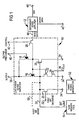
- FIG. 1 there is shown a preferred embodiment of the present invention low power sense amplifier 10 connected to a gain memory cell 14 with a secondary sense amplifier 12 and timing signal generator 52.
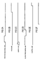
- the timing signal generator 52 provides the signals which are connected to the first bit discharge line 32, the hold line 36, the supply line 38, the output precharge line 40, the control line 42 and the word line. The sequence of the signals are shown in FIG. 2 and their functionality is explained later.
- the low power sense amplifier 10 is implemented utilizing two pMOS transistors 16 and 18 and five nMOS transistors 20, 22, 24, 26 and 28.
- a first bit sense line 30 from the gain memory cell 14 is commonly interconnected to the drain of nMOS transistor 20, the drain of nMOS transistor 22, the gate of nMOS transistor 26, and the drain of pMOS transistor 16.
- a first bit discharge line 32 is coupled to the gate of nMOS transistor 20.
- the source of nMOS transistor 20 is coupled to ground 34.
- the source of nMOS transistor 22 is coupled to the drain of nMOS transistor 24.
- a hold line 36 is coupled to the gate of nMOS transistor 24.
- the source of nMOS transistor 24 and the source of nMOS transistor 26 are coupled to ground 34.
- a supply line 38 is coupled to the source of pMOS transistor 16 and the source of pMOS transistor 18.
- An output precharge line 40 is coupled to the gate of pMOS transistor 18.
- the gate of pMOS transistor 16, the gate of nMOS transistor 22, the drain of pMOS transistor 18, the drain of nMOS transistor 26, and the drain of nMOS transistor 28 are commonly interconnected.
- a control line 42 is connected to the gate of pMOS transistor 28.
- a secondary sense amplifier 12 has a read data line 44, a word data line 46 and a R/W line 48.
- the read data line 44 is connected to the source of nMOS transistor 28.
- the secondary sense amplifier 12 can be a current sensitive differential amplifier connected to the read data line 44 and a reference current source or a voltage differential amplifier connected to the read data line 44 and a reference voltage source.
- the designs of a current sensitive differential amplifier and a voltage differential amplifier are well known to those ordinarily skilled in the art.
- FIG. 2 shows the timing of input signals from the first bit discharge line 32 (FIG. 2A), the hold line 36 (FIG. 2B), the supply line 38 (FIG. 2C), the output precharge line 40 (FIG. 2D), the control line 42 (FIG. 2E) and the word line (FIG. 2F) during a read sensing cycle.
- the input signals are generated by a timing signal generator 52.
- the timing signal generator 52 is constructed from logic gates and timers, electronic components that are well known in the art and can be selected by a person of ordinary skill in the art and from readily available commercial sources.
- the first bit discharge line 32 (FIG. 2A) becomes HIGH and turns nMOS transistor 20 ON which shunts the first bit sense line 30 to ground 34.
- a voltage source V DD is applied to the supply line 38 (FIG. 2C) which turns ON the low power sense amplifier 10 for sensing the signal of a gain memory cell.
- the first bit discharge line 32 (FIG. 2A) now becomes LOW which causes the first bit sense line 30 to float.
- the output precharge line 40 (FIG. 2D) becomes LOW and turns ON pMOS transistor 18 which shunts the drain of nMOS transistor 26 and the commonly connected component terminals to the supply line 38 (FIG. 2C) which has a voltage source V DD currently applied to it.
- the output precharge line 40 (FIG. 2D) now becomes HIGH and turns OFF pMOS transistor 18 which causes the drain of nMOS transistor 26 and the commonly connected component terminals to float.
- the gain memory cell 14 is now activated for sensing by turning ON an appropriate word line (FIG 2F).
- nMOS transistor 24 When the hold line 36 (FIG. 2B) becomes HIGH, nMOS transistor 24 is turned ON. Because nMOS transistor 22 is already ON the first bit sense line 30 is shunted to ground 34. This causes the first bit sense line 30 to remain stable with a LOW value for the duration of the sensing cycle.
- nMOS transistor 24 When the hold line 36 (FIG. 2B) becomes HIGH, nMOS transistor 24 is turned ON. However, because nMOS transistor 22 is OFF the first bit sense line 30 is not shunted to ground 34.
- the low power sense amplifier 10 has two primary modes, an active mode and a stand by mode.
- the low power sense amplifier 10 is in the stand by mode when the supply line 38 (FIG. 2C) is disconnected from the voltage source V DD or when the supply line 38 (FIG. 2C) is connected to ground 34. When operated in the stand by mode no power is consumed by the low power sense amplifier 10.
- the read data line 44 is precharged with voltage source V DD . Then the control line 42 (FIG. 2E) becomes HIGH and nMOS transistor 28 is turned ON which connects the low power sense amplifier 10 to the read data line 44. If the signal from the low power sense amplifier 10 has the value of logical "1" the read data line 44 remains HIGH. If the signal from the low power sense amplifier 10 has the value of logical "0" the read data line 44 is discharged and made LOW.
- an optional second bit sense line 50 reduces in half the number of low power sense amplifiers for a gain memory cell 14 array.
- the second bit sense line 50 represent a greater capacitive load to the low power sense amplifier 10. This increased capacitive load requires an increase of the channel size in nMOS transistor 20 and pMOS transistor 16 in order to provide the necessary increase in current.
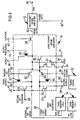
- FIG. 3 there is shown an alternate embodiment of the low power sense amplifier 10.
- the same reference numbers used in FIG. 1 have been retained to refer to the same components.
- the source and the drain of nMOS transistor 60 is connected in series with the first bit sense line 30.
- the source and the drain of nMOS transistor 62 is connected in series with the second bit sense line 50.
- a first bit control line 64 is connected to the gate of nMOS transistor 60.
- a second bit control line 66 is connected to the gate of nMOS transistor 62.
- the drain of nMOS transistor 70 is connected to the second bit sense line 50.
- Second bit discharge line 68 is connected to the gate of nMOS transistor 70.
- the source of nMOS transistor 70 is connected to ground 34.
- the timing signal generator 52 provides the first bit control signal 64, the second bit control signal 66, and the second bit precharge signal 68.
- first bit control line 64 is HIGH
- second bit control line 66 is HIGH
- nMOS transistor 62 is turned ON to connect second bit sense line 50.
- the first bit sense line 30 When the first bit sense line 30 is selected, the first bit sense line 30 is discharged as described before.
- the second bit sense line 50 is selected, the second bit discharge line 68 becomes HIGH to turn nMOS transistor 70 ON which shunts the second bit sense line 50 to ground 34. Further, after the second bit sense line 50 has been discharged, the second bit discharge line 68 becomes LOW to causes the second bit sense line 50 to float.
- the alternate embodiment of the low power sense amplifier 10 reduces the capacitive load by disconnecting either the first bit sense line 30 or the second bit sense line 50. Therefore, an increase of the channel size in nMOS transistor 20 and pMOS transistor 16 is not required.
- nMOS transistor 60 and the gate of nMOS transistor 62 it is necessary for the gate of nMOS transistor 60 and the gate of nMOS transistor 62 to be boosted in order to pass the full level of the signal from the corresponding bit sense line.
- FIG. 4 there is shown an alternate third embodiment of the low power sense amplifier 10.
- the same reference numbers used in FIG. 1 and in FIG. 3 have been retained to refer to the same components.
- the timing signal generator 52 provides the second supply signal 84 and the third supply signal 86.
- the pMOS transistor 16 shown in FIG. 3. has been replaced by separate pMOS transistors 80 and 82.
- the drain of pMOS transistor 80 is connected to the first bit sense line 30.
- the drain of pMOS transistor 82 is connected to the second bit sense line 50.
- the source of pMOS transistor 80 is connected to a second supply line 84.
- the source of pMOS transistor 82 is connected to a third supply line 86.
- the gate of pMOS transistor 80 and the gate of pMOS transistor 82 are connected in common with the drain of pMOS transistor 18, the drain of nMOS transistor 26, the drain of nMOS transistor 28 and the gate of nMOS transistor 22.
- the functioning of the alternate third embodiment of the low power sense amplifier 10 shown in FIG. 4 in relationship to the sequence of input signals is the same as described for the low power sense amplifier 10 shown in FIG. 3 except for the second supply line 84 and the third supply line 86.
- the voltage source V DD is applied to the second supply line 84 when the first bit sense line 30 is selected as previously described.
- the voltage source V DD is applied to the third supply line 86 when the second bit sense line 50 is selected as previously described.
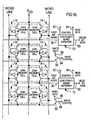
- the low power sense amplifier 10 has a first bit sense line 30, a second bit sense line 50, a control line 42, and a read data line 44.
- the first bit sense line 30 is connected to the array of gain memory cells 14.
- the connection to the second bit sense line 50 to another part of the array of the gain memory cells 14 is not shown for simplicity.
- the source and the drain of nMOS transfer transistor 92 is connected between the write data line signal 96 and the array of gain memory cells 14.
- the gate of the nMOS transfer transistor 92 is connected to the write control line 94.
- Writing into the gain memory cells 14 is accomplished by control of the read data line 44 by the control line 42 or by directly applying the write data line signal 96 to the bit sense line by the appropriate transfer transistor 92 by write control line 94. This results in a very short writing cycle time.
Landscapes
- Engineering & Computer Science (AREA)
- Microelectronics & Electronic Packaging (AREA)
- Computer Hardware Design (AREA)
- Dram (AREA)
- Static Random-Access Memory (AREA)
- Amplifiers (AREA)
- Semiconductor Memories (AREA)
Abstract
Description
- The present invention relates to a memory arrangement comprising a low power CMOS sense amplifier for gain memory cells.
- The output signal from a standard memory cell provides a well defined predetermined voltage difference for both logical states which can be sensed by a standard sense amplifier. A gain memory cell differs from the standard memory cell by not having a well defined voltage difference for both logic states. The gain memory cell will deliver charge only when a logical "1" is present. The output signal from a gain memory cell cannot be. sensed by a standard sense amplifier. The sense amplifier for a gain memory cell must provide a well defined output state for both logical levels "1" and "0" from a charge signal delivered only when a logical "1" is present.
- In designing a sense amplifier, the potential for low-power operation is one of the attractive attributes of CMOS technology. A typical CMOS circuit application can provide very low standby power. Current flows in the circuit only when a transition of state is occurring. This feature makes it extremely easy to manage the power dissipation in CMOS designs. For an n-channel device the current carriers are electrons, whereas for a p-channel device the carriers are holes. Four separate regions or terminals exist in a MOS transistor: source, drain, gate and substrate. For normal operation, the source, drain and gate voltages measured with respect to substrate are positive for an n-channel device and negative for a p-channel device. The output is always connected to one of the power supply rails because at any given state only one transistor is on and the other is off. This guarantees that the logic swing will be determined by the power supply voltage only, and not by the ratio of the effective impedance of the devices, as is the case with static nMOS design.
- The prior art is replete with sense amplifiers for use with memory cells. Some examples of prior art devices are as follows:
- U.S. Patent No. 3,932,848, entitled Feedback Circuit For Allowing Rapid Charging And Discharging Of A Sense Node In A Static Memory, issued to E. Porat, discloses an n-channel sense amplifier which incorporates feedback to a charged sense node. This allows for the rapid charging and discharging necessary to maintain a predetermined signal level. The sense amplifier uses a feedback circuit to control the potential drop of the bit line.
- U.S. Patent No. 4,434,381, entitled Sense Amplifiers, issued to R. G. Stewart, discloses a sense amplifier and concepts related to precharging and setting of sensing transitions. This circuit requires the use of a relatively high number of devices.
- U.S. Patent No. 4,567,387, entitled Linear Sense Amplifier, issued to I. T. Wacyk, discloses a sense amplifier that adds a bias current to the current delivered by the memory device.
- U.S. Patent No. 4,574,365, entitled Shared Access Lines Memory Cells, issued to R. E. Scheuerlein, discloses shared sense amplifiers for coupled memory cells. The memory cells are read out using a sense line, a first and a second bit line.
- U.S. Patent No. 4,970,689, entitled Charge Amplifying Trench Memory Cell, issued to Donald M. Kenney on November 13, 1990, discloses a memory cell with a storage node that is not directly connected to the bit line during a read. The circuit requires two data lines for writing and reading.
- U.S. Patent No. 5,015,890, entitled Sense Amplifier Having Pull-up Circuit Controlled By Feedback, issued to Hiroaki Murakami et al. on May 14, 1991, discloses a sense amplifier for a low signal generated by a conventional memory cell.
- U.S. Patent No. 5,015,891, entitled Output Feedback Control Circuit For Integrated Circuit Device, issued to Yun-ho Choi on May 14, 1991, discloses a sense amplifier consisting of a read driver and an output latch transition block which utilizes a high device count.
- U.S. Patent No. 5,138,198, entitled Intregrated Programmable Logic Device With Control Circuit To Power Down Unused Sense Amplifiers, issued to Ju Shen et al. on August 11, 1992, discloses a logic device which powers down sense amplifiers that are not in use.
- European Patent Application EP 0 603 651 A3 relates to a memory system connected via bit lines to sense amplifiers having at least two pairs of MOS transistors which have opposite conductivity types. The disclosed sense amplifiers are used with gain memory cells.
- A problem typically associated with a sense amplifier for a gain memory cell is that of a relatively high component count. The high component count inflicts a cost and size penalty in the memory circuit and thus limits the operating speed and the density of the memory circuit.
- It is, therefore, desirable to reduce the component count for a sense amplifier for a gain memory cell.
- Another problem with sense amplifiers for gain memory cells is their power consumption both in the active mode and in the stand by mode. This power consumption limits the memory circuit density because of heat dissipation limitations as well as increases the power supply capacity requirements. It is desirable to minimize the power consumption of a sense amplifier for a gain memory cell in both the active mode and the stand by mode of operation.
- It is, therefore, an object of the present invention to provide a sense amplifier which reduces power consumption.
- It is a further object of the present invention to provide a sense amplifier capable of very fast sensing of the output signals of gain memory cells.
- The present invention is a memory arrangement with a low power sense amplifier to sense the output of any memory cell which delivers a signal charge in one logical state and substantially no charge in the other logical state, and is especially suited for use with gain memory cells. The present invention low power sense amplifier circuit is based on an inverter with a feedback loop with additional circuitry providing stability after signal sensing. The bit sense line is discharged before sensing and after sensing it is locked to either a logical "0" or a logical "1" corresponding to the logical value of the gain memory cell during the read sensing cycle. The sense amplifier provides a logic output that is well defined with respect to the supply voltage and corresponds to the logic value of the gain memory cell. The present invention low power sense amplifier has no bias current flow during signal sensing and no power consumption in the stand by mode. The present invention low power sense amplifier is capable of being shared by two bit sense lines. The low power sense amplifier has a relatively low component count which allows for greater memory density and for the amplifier to be capable of very fast sensing of the output signals.
- The present invention low power sense amplifier can be used for a gain memory cell operative in a first state for storing a logical 1 and in a second state for storing a logical 0 wherein the gain memory cell is activated by applying a signal to a control line so that the gain memory cell applies a stored potential to a bit line, the stored potential indicative of a first potential level that corresponds to a stored logical 1 and a second potential level that corresponds to a stored logical 0. The sense amplifier comprises a preliminary discharge means, an actuatable sense amplifier means and an activation means. The preliminary discharge means is coupled to the bit line, for discharging the bit line prior to sensing. The actuatable sense amplifier means is responsive to an actuation control signal to sense a level on the bit line and provide an output signal. The sense amplifier means is coupled to the bit line. The output signal of the sense amplifier means has a first state of a supply voltage in response to the first potential level and a second floating state in response to the second potential level on the bit line. An output line for providing the output signal is being supplied by the supply voltage by means of switching means connected to the supply voltage. The output line is precharged by means of precharge switching means. The activation means is coupled to the control line of the memory gain cell so that the gain memory cell applies the stored potential level to the bit line and for activating the actuatable sense amplifier means to sense the bit line. Wherein the output signal of the actuatable sense amplifier means is operative in the first state when the gain memory cell contains the stored logical 1 and in the second state when the gain memory cell contains the stored logical 0.
- The above objects and further features and advantages of the invention are described in detail below in conjunction with the drawing, of which:
- FIG. 1 shows a schematic diagram of a low power sense amplifier with an optional second bit sense line;
- FIG. 2A shows a timing diagram for a read sensing cycle of first bit discharge line;
- FIG. 2B shows a timing diagram for a read sensing cycle of hold line;
- FIG. 2C shows a timing diagram for a read sensing cycle of supply line;
- FIG. 2D shows a timing diagram for a read sensing cycle of output precharge line;
- FIG. 2E shows a timing diagram for a read sensing cycle of control line;
- FIG. 2F shows a timing diagram for a read sensing cycle of word line;
- FIG. 3 shows a schematic diagram of a low power sense amplifier shared between two bit sense lines with bit sense line switches;
- FIG. 4 shows a schematic diagram of a low power sense amplifier shared by two bit sense lines with bit sense line switches and separate pull-up transistors.
- FIG. 5 shows a schematic diagram of a low power sense amplifiers connected to an array of gain memory cells.
-
- Although the present invention low power sense amplifier can be used to sense the outputs of any memory cell which delivers a signal charge in one logical state and substantially no charge in the other logical state, having only a small voltage difference between both logic states, the present invention is especially suited for use with gain memory cells. Accordingly the present invention low power sense amplifier will be described below in the context of a gain memory cell application in order to describe the best mode of the invention.
- Referring to FIG. 1 there is shown a preferred embodiment of the present invention low
power sense amplifier 10 connected to again memory cell 14 with asecondary sense amplifier 12 andtiming signal generator 52. - The
timing signal generator 52 provides the signals which are connected to the firstbit discharge line 32, thehold line 36, thesupply line 38, theoutput precharge line 40, thecontrol line 42 and the word line. The sequence of the signals are shown in FIG. 2 and their functionality is explained later. - The low
power sense amplifier 10 is implemented utilizing twopMOS transistors nMOS transistors bit sense line 30 from thegain memory cell 14 is commonly interconnected to the drain ofnMOS transistor 20, the drain ofnMOS transistor 22, the gate ofnMOS transistor 26, and the drain ofpMOS transistor 16. A firstbit discharge line 32 is coupled to the gate ofnMOS transistor 20. The source ofnMOS transistor 20 is coupled toground 34. The source ofnMOS transistor 22 is coupled to the drain ofnMOS transistor 24. Ahold line 36 is coupled to the gate ofnMOS transistor 24. The source ofnMOS transistor 24 and the source ofnMOS transistor 26 are coupled toground 34. Asupply line 38 is coupled to the source ofpMOS transistor 16 and the source ofpMOS transistor 18. Anoutput precharge line 40 is coupled to the gate ofpMOS transistor 18. The gate ofpMOS transistor 16, the gate ofnMOS transistor 22, the drain ofpMOS transistor 18, the drain ofnMOS transistor 26, and the drain ofnMOS transistor 28 are commonly interconnected. Acontrol line 42 is connected to the gate ofpMOS transistor 28. - A
secondary sense amplifier 12 has a readdata line 44, aword data line 46 and a R/W line 48. The readdata line 44 is connected to the source ofnMOS transistor 28. - The
secondary sense amplifier 12 can be a current sensitive differential amplifier connected to the readdata line 44 and a reference current source or a voltage differential amplifier connected to the readdata line 44 and a reference voltage source. The designs of a current sensitive differential amplifier and a voltage differential amplifier are well known to those ordinarily skilled in the art. - FIG. 2 shows the timing of input signals from the first bit discharge line 32 (FIG. 2A), the hold line 36 (FIG. 2B), the supply line 38 (FIG. 2C), the output precharge line 40 (FIG. 2D), the control line 42 (FIG. 2E) and the word line (FIG. 2F) during a read sensing cycle.
- Referring back to FIG. 1 in conjunction with FIG. 2, the functioning of the low
power sense amplifier 10 in relationship to the sequence of input signals will be explained. The input signals are generated by atiming signal generator 52. Thetiming signal generator 52 is constructed from logic gates and timers, electronic components that are well known in the art and can be selected by a person of ordinary skill in the art and from readily available commercial sources. The first bit discharge line 32 (FIG. 2A) becomes HIGH and turnsnMOS transistor 20 ON which shunts the firstbit sense line 30 to ground 34. A voltage source VDD is applied to the supply line 38 (FIG. 2C) which turns ON the lowpower sense amplifier 10 for sensing the signal of a gain memory cell. - The first bit discharge line 32 (FIG. 2A) now becomes LOW which causes the first
bit sense line 30 to float. At the same time, the output precharge line 40 (FIG. 2D) becomes LOW and turnsON pMOS transistor 18 which shunts the drain ofnMOS transistor 26 and the commonly connected component terminals to the supply line 38 (FIG. 2C) which has a voltage source VDD currently applied to it. - The output precharge line 40 (FIG. 2D) now becomes HIGH and turns
OFF pMOS transistor 18 which causes the drain ofnMOS transistor 26 and the commonly connected component terminals to float. Thegain memory cell 14 is now activated for sensing by turning ON an appropriate word line (FIG 2F). - When the
gain memory cell 14 has the value of logical "0" no charge is supplied to the firstbit sense line 30 which therefore remains LOW and causes thenMOS transistor 26 to remain OFF, the drain ofnMOS transistor 26 remains charged,pMOS transistor 16 remains OFF andnMOS transistor 22 remains ON. - When the hold line 36 (FIG. 2B) becomes HIGH,
nMOS transistor 24 is turned ON. BecausenMOS transistor 22 is already ON the firstbit sense line 30 is shunted to ground 34. This causes the firstbit sense line 30 to remain stable with a LOW value for the duration of the sensing cycle. - When the
gain memory cell 14 has the value of logical "1" charge is supplied to the firstbit sense line 30 which becomes HIGH and causesnMOS transistor 26 to turn ON. This causes the drain ofnMOS transistor 26 to become LOW which turnsnMOS transistor 22 OFF andpMOS transistor 16 ON which locks the firstbit sense line 30 HIGH. - When the hold line 36 (FIG. 2B) becomes HIGH,
nMOS transistor 24 is turned ON. However, becausenMOS transistor 22 is OFF the firstbit sense line 30 is not shunted to ground 34. - The low
power sense amplifier 10 has two primary modes, an active mode and a stand by mode. The lowpower sense amplifier 10 is in the stand by mode when the supply line 38 (FIG. 2C) is disconnected from the voltage source VDD or when the supply line 38 (FIG. 2C) is connected to ground 34. When operated in the stand by mode no power is consumed by the lowpower sense amplifier 10. - Before the signal from the low
power sense amplifier 10 is transferred to thesecondary sense amplifier 12 theread data line 44 is precharged with voltage source VDD. Then the control line 42 (FIG. 2E) becomes HIGH andnMOS transistor 28 is turned ON which connects the lowpower sense amplifier 10 to the readdata line 44. If the signal from the lowpower sense amplifier 10 has the value of logical "1" theread data line 44 remains HIGH. If the signal from the lowpower sense amplifier 10 has the value of logical "0" theread data line 44 is discharged and made LOW. - Referring back to FIG. 1 there is shown an optional second
bit sense line 50. The addition of the secondbit sense line 50 reduces in half the number of low power sense amplifiers for again memory cell 14 array. However, the secondbit sense line 50 represent a greater capacitive load to the lowpower sense amplifier 10. This increased capacitive load requires an increase of the channel size innMOS transistor 20 andpMOS transistor 16 in order to provide the necessary increase in current. - Referring to FIG. 3 there is shown an alternate embodiment of the low
power sense amplifier 10. The same reference numbers used in FIG. 1 have been retained to refer to the same components. The source and the drain ofnMOS transistor 60 is connected in series with the firstbit sense line 30. The source and the drain ofnMOS transistor 62 is connected in series with the secondbit sense line 50. A firstbit control line 64 is connected to the gate ofnMOS transistor 60. A secondbit control line 66 is connected to the gate ofnMOS transistor 62. The drain ofnMOS transistor 70 is connected to the secondbit sense line 50. Secondbit discharge line 68 is connected to the gate ofnMOS transistor 70. The source ofnMOS transistor 70 is connected to ground 34. - The functioning of the alternate embodiment of the low
power sense amplifier 10 shown in FIG. 3 in relationship to the sequence of input signals is the same as described for the lowpower sense amplifier 10 shown in FIG. 1 except for the selection of the firstbit sense line 30 or the secondbit sense line 50 and the precharging of the corresponding bit sense line. Thetiming signal generator 52 provides the firstbit control signal 64, the secondbit control signal 66, and the second bitprecharge signal 68. When the firstbit control line 64 is HIGH,nMOS transistor 60 is turned ON to connect firstbit sense line 30. When the secondbit control line 66 is HIGH,nMOS transistor 62 is turned ON to connect secondbit sense line 50. - When the first
bit sense line 30 is selected, the firstbit sense line 30 is discharged as described before. When the secondbit sense line 50 is selected, the secondbit discharge line 68 becomes HIGH to turnnMOS transistor 70 ON which shunts the secondbit sense line 50 to ground 34. Further, after the secondbit sense line 50 has been discharged, the secondbit discharge line 68 becomes LOW to causes the secondbit sense line 50 to float. - The alternate embodiment of the low
power sense amplifier 10 reduces the capacitive load by disconnecting either the firstbit sense line 30 or the secondbit sense line 50. Therefore, an increase of the channel size innMOS transistor 20 andpMOS transistor 16 is not required. - However, with the alternate embodiment of the low
power sense amplifier 10 it is necessary for the gate ofnMOS transistor 60 and the gate ofnMOS transistor 62 to be boosted in order to pass the full level of the signal from the corresponding bit sense line. - Referring to FIG. 4 there is shown an alternate third embodiment of the low
power sense amplifier 10. The same reference numbers used in FIG. 1 and in FIG. 3 have been retained to refer to the same components. Thetiming signal generator 52 provides thesecond supply signal 84 and thethird supply signal 86. In the alternate third embodiment of the lowpower sense amplifier 10 thepMOS transistor 16 shown in FIG. 3. has been replaced by separatepMOS transistors 80 and 82. The drain ofpMOS transistor 80 is connected to the firstbit sense line 30. The drain of pMOS transistor 82 is connected to the secondbit sense line 50. The source ofpMOS transistor 80 is connected to asecond supply line 84. The source of pMOS transistor 82 is connected to athird supply line 86. The gate ofpMOS transistor 80 and the gate of pMOS transistor 82 are connected in common with the drain ofpMOS transistor 18, the drain ofnMOS transistor 26, the drain ofnMOS transistor 28 and the gate ofnMOS transistor 22. - The functioning of the alternate third embodiment of the low
power sense amplifier 10 shown in FIG. 4 in relationship to the sequence of input signals is the same as described for the lowpower sense amplifier 10 shown in FIG. 3 except for thesecond supply line 84 and thethird supply line 86. The voltage source VDD is applied to thesecond supply line 84 when the firstbit sense line 30 is selected as previously described. The voltage source VDD is applied to thethird supply line 86 when the secondbit sense line 50 is selected as previously described. - With the alternate third embodiment of the low
power sense amplifier 10 shown in FIG. 4 it is not necessary for the gate ofnMOS transistor 60 or the gate ofnMOS transistor 62 to be boosted in order to pass the full level of the signal from the corresponding bit sense line as was necessary with the low power sense amplifier shown in FIG. 3. - Referring to FIG. 5 there are shown four low
power sense amplifiers 10 connected to an array ofgain memory cells 14. The same reference numbers used in FIG. 1 have been retained to refer to the same components. The lowpower sense amplifier 10 has a firstbit sense line 30, a secondbit sense line 50, acontrol line 42, and aread data line 44. The firstbit sense line 30 is connected to the array ofgain memory cells 14. The connection to the secondbit sense line 50 to another part of the array of thegain memory cells 14 is not shown for simplicity. The source and the drain ofnMOS transfer transistor 92 is connected between the writedata line signal 96 and the array ofgain memory cells 14. The gate of thenMOS transfer transistor 92 is connected to thewrite control line 94. - Writing into the
gain memory cells 14 is accomplished by control of the readdata line 44 by thecontrol line 42 or by directly applying the writedata line signal 96 to the bit sense line by theappropriate transfer transistor 92 bywrite control line 94. This results in a very short writing cycle time. - It should be understood that the embodiments described herein are merely exemplary and that a person skilled in the art may make variations and modifications without departing from the scope of the invention. All such variations and modifications are intended to be included within the scope of the invention as defined in the appended claims.
Claims (15)
- A memory arrangement comprising:characterized in thatat least a gain memory cell (14) operative in a first state for storing a logical 1 and in a second state for storing a logical 0 wherein the gain memory cell (14) is activated by applying a signal to a control line so that the gain memory cell (14) applies a stored potential to a bit line (30), the stored potential indicative of a first potential level that corresponds to a stored logical 1 and a second potential level that corresponds to a stored logical 0,preliminary discharge means (20), coupled to the bit line (30), for discharging the bit line (30) prior to sensing;activation means (52) coupled to the control line of the gain memory cell (14) so that the gain memory cell (14) applies the stored potential level to the bit line (30) and for activating an actuatable amplifier means (10) to sense the bit line (30);the actuatable sense amplifier means (10) responsive to an actuation control signal (38) to sense a level on the bit line (30) and provide an output signal at an output line (44), said sense amplifier means (10) coupled to the bit line (30), said sense amplifier means (10) including feedback means (16, 22, 26) for ensuring a full potential level back to the bit line (30) for each of the first potential level and second potential level,said output line (44) of said sense amplifier means (10) being supplied by a supply voltage (34) by means of switching means (26) connected to a terminal for the supply voltage in response to the first potential level,
the actuatable sense amplifier means (10) include precharge switching means (18) for applying a precharge potential (38) to said output line which is being in a floating condition in response to the second potential level on the bit line (30). - The memory arrangement as recited in claim 1, wherein said preliminary discharge means (20) comprises an nMOS transistor having a source, a drain and a gate electrode, with said source electrode adapted to receive a first potential (34), said drain electrode coupled to the bit line (30), and said gate electrode coupled to a preliminary discharge control line (32).
- The memory arrangement as recited in claim 1, further comprising switching means (28) adapted to receive said output signal of said actuatable sense amplifier means (10) for providing a switched output signal in response to a switch control signal (42).
- The memory arrangement as recited in claim 3, wherein said switching means (28) comprises an nMOS transistor having a source, a drain and a gate electrode, with said drain electrode adapted to receive said output signal of said actuatable sense amplifier means (10), said gate electrode adapted to receive a switch control signal (42).
- The memory arrangement as recited in claim 1, wherein said actuatable sense means (10) further comprises:a first nMOS transistor (26), having a drain, a source and a gate electrode,
said gate electrode coupled to the bit line (30), said source electrode coupled to the first potential (34);a second nMOS transistor (22), having a drain, a source and a gate electrode, said drain electrode coupled to the bit line (30);a third nMOS transistor (24), having a drain, a source and a gate electrode, said drain electrode coupled to said source electrode of said second nMOS transistor (22), said source electrode coupled to said first potential (34), said gate adapted to receive a hold signal (36);a first pMOS transistor (16) having a drain, source and a gate electrode, said source electrode coupled to a second potential (38), said drain electrode coupled to the bit line (30);a second pMOS transistor (18), having a drain, a source and a gate electrode, said source electrode coupled to said second potential (38), said gate electrode adapted to receive a precharge control signal (40);the output line (44) commonly coupled to said gate electrode of said first pMOS transistor (16), said drain electrode of said second pMOS transistor (18), said gate electrode of said second nMOS transistor (22), and said drain electrode of said first nMOS transistor (26). - The memory arrangement as recited in claim 5, wherein said sense amplifier (10) has an active mode and a stand by mode, wherein said second potential (38) is equivalent to said first potential (34) in said stand by mode, whereby said sense amplifier (10) utilizes no power in said stand by mode.
- The memory arrangement as recited in anyone of claims 1 to 6, comprising:a plurality of gain memory cells (14);a shared bit line commonly interconnected to the bit line (30, 50) of each gain memory cell (14) of the plurality of gain memory cells (14);the activation means (52) coupled to the control line of a selected one of the plurality gain memory cells (14) so that said selected one of the plurality of gain memory cells (14) applies the stored potential level to said shared bit line and for activating said actuatable amplifier means (10) to sense said shared bit line.
- The memory arrangement as recited in claim 7, wherein said shared bit line is interconnected to the bit line (30, 50) of each gain memory cell (14) of the plurality of gain memory cells (14) by a plurality of switching means (60, 62) for switching said interconnection.
- The memory arrangement as recited in claim 8, wherein a plurality of discharge means (20, 70) is connected to the bit line (30, 50) of each one of the gain memory cells (14) of the plurality of gain memory cells (14) before said active switching means (60, 62).
- The memory arrangement as recited in claims 8 or 9,
wherein each of said plurality of switching means (60, 62) comprises an nMOS transistor having a drain, a source and a gate electrode, said source electrode coupled to the bit line (30, 50) of one of the gain memory cells (14) of the plurality of gain memory cells (14), said drain electrode coupled to said shared bit line, and said gate electrode adapted to receive a bit control signal (64, 66). - The memory arrangement as recited in claim 9, wherein each of said plurality of active discharge means (20, 70) comprises an nMOS transistor having a source, a drain and a gate electrode, wherein said source electrode coupled to the first potential (34), said drain electrode coupled to the bit line (30, 50) of one of the plurality of gain memory cells (14), and said gate electrode adapted to receive a preliminary discharge control signal (68, 32).
- The memory arrangement as recited in claim 7, wherein said plurality of gain memory cells (14) commonly interconnected to said shared bit line comprises two gain memory cells (14).
- A method for sensing at least a gain memory cell (14) operative in a first state for storing a logical 1 and in a second state for storing a logical 0 wherein the gain memory cell (14) is activated by applying a signal to a memory control line so that the gain memory cell (14) applies a stored potential to a bit line (30), the potential operative in a first state that corresponds to the stored logical 1 and a second state that corresponds to the stored logical 0, the method comprising the steps of:characterized infirst discharging the bit line (30) in response to a control signal (32);applying a signal to the memory control line so that the gain memory cell (14) applies the potential to the bit line (30);then activating feedback means (16, 22, 26) for ensuring a full potential level back to the bit line (30) for the potential operative in each of the first state and second state ,providing an output signal operating in a state of a supply voltage (34) in response to the first state of the potential,
precharging an output line (44) for said output signal and providing the output signal operating in a floating state in response to the second state of the potential. - The method as recited in claim 13 further comprising the step of latching said output signal for a predetermined period.
- The method as recited in claim 13, wherein the step of first discharging the bit line (30) in response to a control signal (32) comprises an nMOS transistor having a source, a drain and a gate, wherein said source connected to a first potential (34), said drain connected to the bit line (30), and said gate connected to a preliminary discharge control line.
Applications Claiming Priority (2)
| Application Number | Priority Date | Filing Date | Title |
|---|---|---|---|
| US41409095A | 1995-03-31 | 1995-03-31 | |
| US414090 | 1995-03-31 |
Publications (3)
| Publication Number | Publication Date |
|---|---|
| EP0735540A2 EP0735540A2 (en) | 1996-10-02 |
| EP0735540A3 EP0735540A3 (en) | 1996-10-30 |
| EP0735540B1 true EP0735540B1 (en) | 2002-06-19 |
Family
ID=23639918
Family Applications (1)
| Application Number | Title | Priority Date | Filing Date |
|---|---|---|---|
| EP96104548A Expired - Lifetime EP0735540B1 (en) | 1995-03-31 | 1996-03-21 | Low power sense amplifier for gain memory cells |
Country Status (7)
| Country | Link |
|---|---|
| US (1) | US5610540A (en) |
| EP (1) | EP0735540B1 (en) |
| JP (1) | JPH08287692A (en) |
| KR (1) | KR100417479B1 (en) |
| AT (1) | ATE219599T1 (en) |
| DE (1) | DE69621870T2 (en) |
| TW (1) | TW315541B (en) |
Families Citing this family (10)
| Publication number | Priority date | Publication date | Assignee | Title |
|---|---|---|---|---|
| US5734275A (en) * | 1996-07-18 | 1998-03-31 | Advanced Micro Devices, Inc. | Programmable logic device having a sense amplifier with virtual ground |
| US5929660A (en) * | 1997-12-29 | 1999-07-27 | United Technologies Corporation | Dynamic, single-ended sense amplifier |
| JP2002083493A (en) * | 2000-09-05 | 2002-03-22 | Toshiba Corp | Semiconductor memory |
| US6753719B2 (en) * | 2002-08-26 | 2004-06-22 | Motorola, Inc. | System and circuit for controlling well biasing and method thereof |
| JP5518409B2 (en) | 2009-09-15 | 2014-06-11 | ピーエスフォー ルクスコ エスエイアールエル | Semiconductor device, semiconductor memory device, and information processing system including semiconductor device |
| FR2953643B1 (en) * | 2009-12-08 | 2012-07-27 | Soitec Silicon On Insulator | MEMORY CELL FLASH ON SEOI HAVING A SECOND CHECK GRID ENTERREE UNDER THE INSULATING LAYER |
| FR2957449B1 (en) | 2010-03-11 | 2022-07-15 | S O I Tec Silicon On Insulator Tech | READOUT MICRO-AMPLIFIER FOR MEMORY |
| KR101288216B1 (en) | 2011-09-23 | 2013-07-18 | 삼성전기주식회사 | Power amplifier |
| JP2014142995A (en) * | 2014-04-02 | 2014-08-07 | Ps4 Luxco S A R L | Semiconductor device, semiconductor memory and information processing system including semiconductor device |
| CN108806742B (en) * | 2017-05-04 | 2022-01-04 | 汤朝景 | Random access memory and having circuitry, methods and apparatus associated therewith |
Family Cites Families (13)
| Publication number | Priority date | Publication date | Assignee | Title |
|---|---|---|---|---|
| US3932848A (en) * | 1975-01-20 | 1976-01-13 | Intel Corporation | Feedback circuit for allowing rapid charging and discharging of a sense node in a static memory |
| JPS5836503B2 (en) * | 1980-01-25 | 1983-08-09 | 株式会社東芝 | semiconductor memory device |
| US4434381A (en) * | 1981-12-07 | 1984-02-28 | Rca Corporation | Sense amplifiers |
| US4574365A (en) * | 1983-04-18 | 1986-03-04 | International Business Machines Corporation | Shared access lines memory cells |
| US4567387A (en) * | 1983-06-30 | 1986-01-28 | Rca Corporation | Linear sense amplifier |
| JPS6254893A (en) * | 1985-09-03 | 1987-03-10 | Nec Corp | Semiconductor memory |
| US4970689A (en) * | 1988-03-07 | 1990-11-13 | International Business Machines Corporation | Charge amplifying trench memory cell |
| KR910008101B1 (en) * | 1988-12-30 | 1991-10-07 | 삼성전자 주식회사 | Feedback type data output circuit of semiconductor memory device |
| JPH0814995B2 (en) * | 1989-01-27 | 1996-02-14 | 株式会社東芝 | Semiconductor memory |
| US5013943A (en) * | 1989-08-11 | 1991-05-07 | Simtek Corporation | Single ended sense amplifier with improved data recall for variable bit line current |
| US5138198A (en) * | 1991-05-03 | 1992-08-11 | Lattice Semiconductor Corporation | Integrated programmable logic device with control circuit to power down unused sense amplifiers |
| TW223172B (en) * | 1992-12-22 | 1994-05-01 | Siemens Ag | Siganl sensing circuits for memory system using dynamic gain memory cells |
| US5426385A (en) * | 1994-06-07 | 1995-06-20 | National Science Council | Double positive feedback loop precharge CMOS single-ended sense amplifier |
-
1996
- 1996-03-21 AT AT96104548T patent/ATE219599T1/en active
- 1996-03-21 DE DE69621870T patent/DE69621870T2/en not_active Expired - Fee Related
- 1996-03-21 EP EP96104548A patent/EP0735540B1/en not_active Expired - Lifetime
- 1996-03-22 TW TW085103483A patent/TW315541B/zh not_active IP Right Cessation
- 1996-03-28 KR KR1019960008696A patent/KR100417479B1/en not_active IP Right Cessation
- 1996-04-01 US US08/625,840 patent/US5610540A/en not_active Expired - Lifetime
- 1996-04-01 JP JP8079249A patent/JPH08287692A/en active Pending
Also Published As
| Publication number | Publication date |
|---|---|
| TW315541B (en) | 1997-09-11 |
| EP0735540A3 (en) | 1996-10-30 |
| ATE219599T1 (en) | 2002-07-15 |
| DE69621870D1 (en) | 2002-07-25 |
| KR960035644A (en) | 1996-10-24 |
| EP0735540A2 (en) | 1996-10-02 |
| US5610540A (en) | 1997-03-11 |
| DE69621870T2 (en) | 2003-01-02 |
| JPH08287692A (en) | 1996-11-01 |
| KR100417479B1 (en) | 2004-04-29 |
Similar Documents
| Publication | Publication Date | Title |
|---|---|---|
| US10482952B2 (en) | Integrated circuit with separate supply voltage for memory that is different from logic circuit supply voltage | |
| US5258950A (en) | Semiconductor memory device | |
| US6492863B2 (en) | Internal high voltage generation circuit capable of stably generating internal high voltage and circuit element therefor | |
| US5734604A (en) | Static random access memory capable of both reducing power consumption and retaining data at standby-time | |
| JP2009151932A (en) | Low-power high-performance memory circuit and related method | |
| JP2006500702A5 (en) | ||
| US5793671A (en) | Static random access memory cell utilizing enhancement mode N-channel transistors as load elements | |
| EP0821364B1 (en) | Sense circuit | |
| KR19990036155A (en) | Charge transfer sense amplifier | |
| EP0735540B1 (en) | Low power sense amplifier for gain memory cells | |
| US5532969A (en) | Clocking circuit with increasing delay as supply voltage VDD | |
| US6362661B1 (en) | Sense amplifier for use in a semiconductor memory device | |
| EP0439154A2 (en) | Semiconductor memory device and data processing device using same | |
| US7046565B1 (en) | Bi-mode sense amplifier with dual utilization of the reference cells and dual precharge scheme for improving data retention | |
| GB2300282A (en) | Substrate bias voltage control circuit | |
| US20040017713A1 (en) | Ferroelectric memory supplying predetermined amount of direct-current bias electricity to first and second bit lines upon reading data from memory cell | |
| CA1169964A (en) | Decoder circuit for semiconductor memory | |
| US6898136B2 (en) | Semiconductor memory device, capable of reducing power consumption | |
| JP2003510754A (en) | Zero power precharge SRAM | |
| US20010026189A1 (en) | Intermediate voltage control circuit having reduced power consumption five | |
| US5768200A (en) | Charging a sense amplifier | |
| KR100256295B1 (en) | Circuit of sram |
Legal Events
| Date | Code | Title | Description |
|---|---|---|---|
| PUAI | Public reference made under article 153(3) epc to a published international application that has entered the european phase |
Free format text: ORIGINAL CODE: 0009012 |
|
| PUAL | Search report despatched |
Free format text: ORIGINAL CODE: 0009013 |
|
| AK | Designated contracting states |
Kind code of ref document: A2 Designated state(s): AT DE FR GB IE IT NL |
|
| AK | Designated contracting states |
Kind code of ref document: A3 Designated state(s): AT DE FR GB IE IT NL |
|
| 17P | Request for examination filed |
Effective date: 19970522 |
|
| 17Q | First examination report despatched |
Effective date: 19991221 |
|
| RAP1 | Party data changed (applicant data changed or rights of an application transferred) |
Owner name: INFINEON TECHNOLOGIES AG |
|
| GRAG | Despatch of communication of intention to grant |
Free format text: ORIGINAL CODE: EPIDOS AGRA |
|
| GRAG | Despatch of communication of intention to grant |
Free format text: ORIGINAL CODE: EPIDOS AGRA |
|
| GRAH | Despatch of communication of intention to grant a patent |
Free format text: ORIGINAL CODE: EPIDOS IGRA |
|
| GRAH | Despatch of communication of intention to grant a patent |
Free format text: ORIGINAL CODE: EPIDOS IGRA |
|
| GRAA | (expected) grant |
Free format text: ORIGINAL CODE: 0009210 |
|
| AK | Designated contracting states |
Kind code of ref document: B1 Designated state(s): AT DE FR GB IE IT NL |
|
| PG25 | Lapsed in a contracting state [announced via postgrant information from national office to epo] |
Ref country code: NL Free format text: LAPSE BECAUSE OF FAILURE TO SUBMIT A TRANSLATION OF THE DESCRIPTION OR TO PAY THE FEE WITHIN THE PRESCRIBED TIME-LIMIT Effective date: 20020619 Ref country code: IT Free format text: LAPSE BECAUSE OF FAILURE TO SUBMIT A TRANSLATION OF THE DESCRIPTION OR TO PAY THE FEE WITHIN THE PRE;WARNING: LAPSES OF ITALIAN PATENTS WITH EFFECTIVE DATE BEFORE 2007 MAY HAVE OCCURRED AT ANY TIME BEFORE 2007. THE CORRECT EFFECTIVE DATE MAY BE DIFFERENT FROM THE ONE RECORDED.SCRIBED TIME-LIMIT Effective date: 20020619 Ref country code: FR Free format text: LAPSE BECAUSE OF FAILURE TO SUBMIT A TRANSLATION OF THE DESCRIPTION OR TO PAY THE FEE WITHIN THE PRESCRIBED TIME-LIMIT Effective date: 20020619 Ref country code: AT Free format text: LAPSE BECAUSE OF FAILURE TO SUBMIT A TRANSLATION OF THE DESCRIPTION OR TO PAY THE FEE WITHIN THE PRESCRIBED TIME-LIMIT Effective date: 20020619 |
|
| REF | Corresponds to: |
Ref document number: 219599 Country of ref document: AT Date of ref document: 20020715 Kind code of ref document: T |
|
| REG | Reference to a national code |
Ref country code: GB Ref legal event code: FG4D |
|
| REG | Reference to a national code |
Ref country code: IE Ref legal event code: FG4D |
|
| REF | Corresponds to: |
Ref document number: 69621870 Country of ref document: DE Date of ref document: 20020725 |
|
| NLV1 | Nl: lapsed or annulled due to failure to fulfill the requirements of art. 29p and 29m of the patents act | ||
| EN | Fr: translation not filed | ||
| PG25 | Lapsed in a contracting state [announced via postgrant information from national office to epo] |
Ref country code: IE Free format text: LAPSE BECAUSE OF NON-PAYMENT OF DUE FEES Effective date: 20030321 Ref country code: GB Free format text: LAPSE BECAUSE OF NON-PAYMENT OF DUE FEES Effective date: 20030321 |
|
| PLBE | No opposition filed within time limit |
Free format text: ORIGINAL CODE: 0009261 |
|
| STAA | Information on the status of an ep patent application or granted ep patent |
Free format text: STATUS: NO OPPOSITION FILED WITHIN TIME LIMIT |
|
| 26N | No opposition filed |
Effective date: 20030320 |
|
| GBPC | Gb: european patent ceased through non-payment of renewal fee |
Effective date: 20030321 |
|
| REG | Reference to a national code |
Ref country code: IE Ref legal event code: MM4A |
|
| REG | Reference to a national code |
Ref country code: HK Ref legal event code: WD Ref document number: 1003742 Country of ref document: HK |
|
| PGFP | Annual fee paid to national office [announced via postgrant information from national office to epo] |
Ref country code: DE Payment date: 20080510 Year of fee payment: 13 |
|
| PG25 | Lapsed in a contracting state [announced via postgrant information from national office to epo] |
Ref country code: DE Free format text: LAPSE BECAUSE OF NON-PAYMENT OF DUE FEES Effective date: 20091001 |