EP0735501A2 - Arrangement de senseurs de couleur pour lire des marquages en couleur - Google Patents
Arrangement de senseurs de couleur pour lire des marquages en couleur Download PDFInfo
- Publication number
- EP0735501A2 EP0735501A2 EP96103880A EP96103880A EP0735501A2 EP 0735501 A2 EP0735501 A2 EP 0735501A2 EP 96103880 A EP96103880 A EP 96103880A EP 96103880 A EP96103880 A EP 96103880A EP 0735501 A2 EP0735501 A2 EP 0735501A2
- Authority
- EP
- European Patent Office
- Prior art keywords
- sensor arrangement
- radiation
- semiconductor radiation
- color sensor
- receiving
- Prior art date
- Legal status (The legal status is an assumption and is not a legal conclusion. Google has not performed a legal analysis and makes no representation as to the accuracy of the status listed.)
- Granted
Links
- 230000003287 optical effect Effects 0.000 claims abstract description 28
- 230000005855 radiation Effects 0.000 claims description 62
- 239000004065 semiconductor Substances 0.000 claims description 40
- 230000005693 optoelectronics Effects 0.000 claims description 10
- 230000005540 biological transmission Effects 0.000 claims description 8
- 238000013461 design Methods 0.000 claims description 7
- 238000011156 evaluation Methods 0.000 claims description 5
- 230000003595 spectral effect Effects 0.000 claims description 3
- 230000000295 complement effect Effects 0.000 claims 1
- 239000002184 metal Substances 0.000 abstract description 3
- 239000007787 solid Substances 0.000 abstract 1
- 241000219739 Lens Species 0.000 description 36
- 238000013459 approach Methods 0.000 description 8
- 230000008901 benefit Effects 0.000 description 5
- 238000000576 coating method Methods 0.000 description 4
- 239000011248 coating agent Substances 0.000 description 3
- 239000003086 colorant Substances 0.000 description 3
- 239000011521 glass Substances 0.000 description 3
- 238000000034 method Methods 0.000 description 3
- 230000015572 biosynthetic process Effects 0.000 description 2
- 238000005755 formation reaction Methods 0.000 description 2
- 238000012544 monitoring process Methods 0.000 description 2
- 241001136792 Alle Species 0.000 description 1
- 240000004322 Lens culinaris Species 0.000 description 1
- 230000004308 accommodation Effects 0.000 description 1
- 230000006978 adaptation Effects 0.000 description 1
- 230000000903 blocking effect Effects 0.000 description 1
- 238000010276 construction Methods 0.000 description 1
- 238000011109 contamination Methods 0.000 description 1
- 238000010586 diagram Methods 0.000 description 1
- 238000006073 displacement reaction Methods 0.000 description 1
- 230000002349 favourable effect Effects 0.000 description 1
- 238000005286 illumination Methods 0.000 description 1
- 238000002347 injection Methods 0.000 description 1
- 239000007924 injection Substances 0.000 description 1
- 239000004922 lacquer Substances 0.000 description 1
- 238000012545 processing Methods 0.000 description 1
- 210000001747 pupil Anatomy 0.000 description 1
- 230000000717 retained effect Effects 0.000 description 1
- 229920006395 saturated elastomer Polymers 0.000 description 1
- 238000000926 separation method Methods 0.000 description 1
- 230000001629 suppression Effects 0.000 description 1
- 238000012549 training Methods 0.000 description 1
- 230000007704 transition Effects 0.000 description 1
- 238000007740 vapor deposition Methods 0.000 description 1
Images
Classifications
-
- G—PHYSICS
- G01—MEASURING; TESTING
- G01J—MEASUREMENT OF INTENSITY, VELOCITY, SPECTRAL CONTENT, POLARISATION, PHASE OR PULSE CHARACTERISTICS OF INFRARED, VISIBLE OR ULTRAVIOLET LIGHT; COLORIMETRY; RADIATION PYROMETRY
- G01J3/00—Spectrometry; Spectrophotometry; Monochromators; Measuring colours
- G01J3/46—Measurement of colour; Colour measuring devices, e.g. colorimeters
- G01J3/50—Measurement of colour; Colour measuring devices, e.g. colorimeters using electric radiation detectors
- G01J3/501—Colorimeters using spectrally-selective light sources, e.g. LEDs
-
- G—PHYSICS
- G01—MEASURING; TESTING
- G01J—MEASUREMENT OF INTENSITY, VELOCITY, SPECTRAL CONTENT, POLARISATION, PHASE OR PULSE CHARACTERISTICS OF INFRARED, VISIBLE OR ULTRAVIOLET LIGHT; COLORIMETRY; RADIATION PYROMETRY
- G01J3/00—Spectrometry; Spectrophotometry; Monochromators; Measuring colours
- G01J3/02—Details
- G01J3/0205—Optical elements not provided otherwise, e.g. optical manifolds, diffusers, windows
- G01J3/0208—Optical elements not provided otherwise, e.g. optical manifolds, diffusers, windows using focussing or collimating elements, e.g. lenses or mirrors; performing aberration correction
-
- G—PHYSICS
- G01—MEASURING; TESTING
- G01J—MEASUREMENT OF INTENSITY, VELOCITY, SPECTRAL CONTENT, POLARISATION, PHASE OR PULSE CHARACTERISTICS OF INFRARED, VISIBLE OR ULTRAVIOLET LIGHT; COLORIMETRY; RADIATION PYROMETRY
- G01J3/00—Spectrometry; Spectrophotometry; Monochromators; Measuring colours
- G01J3/02—Details
- G01J3/0256—Compact construction
-
- G—PHYSICS
- G06—COMPUTING; CALCULATING OR COUNTING
- G06K—GRAPHICAL DATA READING; PRESENTATION OF DATA; RECORD CARRIERS; HANDLING RECORD CARRIERS
- G06K7/00—Methods or arrangements for sensing record carriers, e.g. for reading patterns
- G06K7/10—Methods or arrangements for sensing record carriers, e.g. for reading patterns by electromagnetic radiation, e.g. optical sensing; by corpuscular radiation
- G06K7/12—Methods or arrangements for sensing record carriers, e.g. for reading patterns by electromagnetic radiation, e.g. optical sensing; by corpuscular radiation using a selected wavelength, e.g. to sense red marks and ignore blue marks
Definitions
- the invention relates to a color sensor arrangement for reading colored markings according to the preamble of claim 1.
- Such color sensor arrangements are particularly preferably used for reading colored print marks in a short working distance.
- the color sensor arrangement is also suitable for many other applications. Reference should be made here to the order control or monitoring of dispensing processes (security lacquer), banderole, label or marking recognition and the monitoring of coating processes. It can also be used for checking the presence of objects. In general, two versions with 10 mm or 60 mm scanning distance are available.
- the aim of the invention is to develop such a color sensor arrangement in such a way that they are compatible with existing contrast sensors with a short scanning range and the housing dimensions of a contrast sensor are retained as far as possible, that is to say that the larger number of optical and optoelectronic components in a color sensor arrangement takes up as little space as possible is housed, but the high demands on the precision of the arrangement of the optical and optoelectronic components are fully met.
- an autocollimation arrangement is therefore used, a geometric beam splitter being used to reduce the optical crosstalk.
- the optical crosstalk is also reduced due to the contamination of the outwardly lying objective lens surface within the illumination cone as a result of the preferably central shadowing.
- the objective is further preferably antireflected on both sides over the entire spectral bandwidth of the semiconductor radiation sources used.
- the geometric beam splitter is advantageously designed according to claim 2, wherein the mirror covering can be arranged according to claims 3 or 4.
- the transmitted light beams of the semiconductor radiation sources pass through the plate, while the received light is reflected from the mirror coating to the receiving arrangement.
- a structurally particularly compact arrangement is achieved by the measures according to claims 5 and 6. In this way, the advantages of using dichroic mirrors are achieved with a compact structure.
- a design with three semiconductor radiation sources in the three primary colors, which are expediently arranged according to claim 7, is particularly advantageous in order to provide compact accommodation on the one hand and the same optical appearance on the other To achieve ways for the radiation of the various semiconductor radiation sources. This is advantageously carried out according to claim 8.
- the measure according to claim 9 advantageously achieves a concentration of the transmitted light on the beam splitter, which benefits on the one hand an exact geometric radiation separation and on the other hand a favorable energy balance.
- the diaphragms according to claim 10 are expediently provided according to the invention.
- the design according to claims 13 or 14 is advantageous, because then the individual components are inserted from the open side into suitably arranged grooves in the tube produced as a precision injection-molded part with a receptacle attachment and thus arranged precisely before the lid is attached can then be fixed in this precision arrangement of the individual components by applying the cover. Applying the lid creates a closed box that only contains five side openings for the three LEDs, the receiver and the lens.
- Circular lenses can be included in this system by training according to claim 16.
- the compact design of the color sensor arrangement according to the invention is further promoted by the design according to claim 17.
- the space that is freed up by the narrower transmission light bundle compared to the reception light bundle is used for accommodating the printed circuit boards.
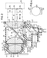
- the core of the color sensor arrangement according to the invention is a tube 36 with a lower receiving projection 37, which are arranged in a rectangular housing 21 made of metal, which can be opened in a suitable manner to introduce the optical, optoelectronic and electronic components to be able to.
- the tube 36 and the receiving projection 37 are preferably designed as a uniform precision injection molded component.
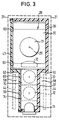
- she 3 have essentially the shape of a box open on one side, which is closed by a cover 43.
- the receiving attachment 37 is, however, significantly narrower than the tube 36, so that at the transition from the receiving attachment 37 to the tube 36 the box has a step 59 and the cover 43 has a step 62.
- the tube 36 has a central cavity 51 which is open at both ends and in which, in FIG. 2, from left to right, one after the other is accommodated: a photo element 26, an annular aperture 25, a lens 24, an IR cut filter 52, a further lens 23 with a larger diameter and a transparent plane-parallel plate 30 inclined at 45 ° to the axis 29 of the condenser lens system 23, 24 or the tube 36, which in the region of the point of intersection of the axis 29 and around it on the side facing away from the condenser lens system 23, 24 a mirror covering 31 is covered.
- the plate 30 with the mirror covering 31 forms a geometric beam splitter 28.
- annular mirror covering 31 ′ which is only indicated by dashed lines in FIG. 2, is provided on the opposite side from the mirror covering 31. It covers those areas of the plate 30 which are permeable in the exemplary embodiment shown in solid lines according to FIG. 2, while in the alternative embodiment the central area which is covered by the mirror covering 31 according to FIG. 2 is permeable.
- a collimator lens 32 is arranged, to which the cavity 42 of the receptacle attachment 37, which is integral with the tube 36, is connected at the bottom.
- two dichroic deflecting mirrors 14 and 15 are arranged at an angle of 45 ° to the axis 16 on its optical axis 16 at a vertical distance.
- the dichroic mirrors 14, 15 are held on the outer walls of the cavity 42 by suitable holders 41 (FIG. 2).
- a receiving space 38 for a further semiconductor radiation source 11 is formed below the dichroic mirror 14, which, for example, emits light in the red spectral range.
- perforated screens 33, 34 and 35 are arranged in the receiving cavities 38, 39, 40, which are concentric with the axis 16 and the axes 53, 54 of the semiconductor radiation sources 12, 13.
- the openings of the perforated screens 38, 39, 40 are rectangular at smaller scanning distances A (FIG. 2) corresponding to the print marks to be recognized and circular at larger scanning distances A.
- a reading area 18 In front of the lens 22 or the housing 21 there is a reading area 18 in which there is an object 20 provided with different color markings 19a, 19b or 19c, the color markings of which are different from those of the invention Color sensor arrangement to be read or recognized.
- the dichroic mirrors 14, 15, the geometric beam splitter 28 and the IR cut filter 52 have a rectangular shape.
- the lenses 23, 24 and 32 are of round design and have rectangular projections 23 ', 23' '(FIGS. 2 and 4), 24', 24 '' and 32 ', 32' 'on two sides, but for optical purposes Do not contribute the image, but perform a pure support function. All of the aforementioned components and also the perforated diaphragms 33, 34, 35 are inserted from the open side into mounting grooves 41 and 57 and pushed in as far as they will go.
- the cover 43 contains corresponding stop formations 60 (FIG. 3) which extend into the tube 36 or the receiving attachment 37 and adjoin the respective optical element, so that after the tube 36 and the receiving attachment 37 have been fully equipped and the clean closing of the cover 43 ensures a correct position of the optical components.
- the lens 22 is circular and inserted into the wall of the housing 21, which is preferably made of metal.
- the tube 36 and the receiving projection 37 are aligned with the housing 21 by means of fitting bores 61 and not shown fitting pins provided on the housing 21.
- the plate 30, which is preferably made of glass, merely serves as a support for the deflecting mirror covering 31 or 31 'and guarantees the correct position of the deflecting mirror in the beam path. 2, the glass plate 30 ends at the top clearly below the upper end of the tube in order to enable a compact relative arrangement of the tube 36 and the objective 22. In order to avoid disturbing reflections, in particular the upper end face of the plate 30 is blackened.
- the lens system 23, 24 is constructed in two stages because a short focal length is to be realized in the present large lens opening.
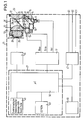
- the photo element 16 is connected via a preamplifier 45 to an evaluation electronics 27, which has a microprocessor 50, an EEPROM 48 and an operating panel 49 with a function switch, tolerance switch, display LEDs and a teach button.
- the evaluation electronics 27 is fed by a power supply unit 46.
- An output stage 47 connected to the microprocessor 50 supplies the output signals of the color sensor arrangement to output terminals Q1, Q2 and Q3.
- the signals at the output terminals Q1 to Q3 represent three switching outputs.
- the overall color sensor arrangement is designed in such a way that up to three different color patterns can be stored per teach-in, i.e. that the sensor can sort three different colors.
- the corresponding switching output Q1, Q2 or Q3 is activated accordingly by the electronics.
- the semiconductor radiation sources 11, 12, 13 are connected to control electronics 17, which in turn are connected to the microprocessor 50.
- FIG. 3 the electrical and electronic components shown in a schematic, extended block diagram in FIG. 1 are arranged on printed circuit boards 44 which are only indicated by dashed lines and which are accommodated in a very compact design to the side of the receiving attachment 37 in rooms 58 of the cuboid housing 21.
- a further printed circuit board 44 can also be arranged flat, according to FIG. 2, directly behind the photoelement 26 on the left end face of the tube 36 in FIG. 2.
- the semiconductor radiation sources 11, 12, 13 are actuated sequentially by the control electronics 17 such that first the semiconductor radiation source 11 is a red light beam, then the semiconductor radiation source 12 is a green light beam and finally the semiconductor radiation source 13 is a blue light beam along the axes 16, 53 and 54 send out.
- the microprocessor 50 generates pulse widths of less than 10 ⁇ s.
- the successively generated light beams of the semiconductor radiation sources 11, 12 and 13 are directed by means of the dichroic mirrors 14, 15 onto the common optical axis 16, with a suitable length of the receiving cavities 38, 39 and 40, 40 'ensuring that the of Cover the radiation emanating from the semiconductor radiation sources 11, 12 and 13 as far as the collimator lens 32.
- the semiconductor radiation sources 11, 12, 13 used have small radiation angles according to the invention, so that narrowly limited radiation beams are emitted, which are further concentrated on the mirror coating 31 of the beam splitter 23 by the collimator lens 32.
- the transmitted light bundles are deflected by 90 ° in the direction of the optical axis 29 of the objective 22. In this way, a transmitted light bundle 55 extends from the objective 22.
- the collimator lens 32 and the objective 22 form the diaphragms 33, 34, 35 arranged directly in front of the semiconductor radiation sources 11, 12, 13 on the surface of an object 20, which is arranged in the reading area 18 located in front of the housing 21 and bears the color markings 19a, 19b and 19c to be read.
- the transmission light bundles are scattered back from the surface of the object 20 to the lens 22, the part 56 of the reception light bundle which takes up the entire cross section of the lens 22 and which does not fall on the central mirror covering 31, passes through the transparent plate 30 and over the lens system 23. 24 strikes the photo element 26, in front of which the diaphragm 25 is arranged with a square opening.
- the length of the plate 30 upwards is essentially limited by the upper end of the mirror covering 31, so that part of the reception light reaches the lens system 23, 24 at the top past the plate 30.
- the likewise square photo element 26 thus emits an electrical signal which is representative of the light intensity received.
- the electrical signal emitted by the photo element 26 is first amplified in the preamplifier 45 (FIG. 1) and fed to a sample and hold stage and is passed via an analog-digital converter for further digital processing.
- the taught-in signal levels or the upper and lower threshold values calculated from them (corresponding to the selected tolerance and hysteresis) and the system software are stored in the EEPROM 48.
- the receiver delivers the same signal level for all three transmission pulses for a given gray value pattern (eg 90% remission). For any color template, it is checked in RUN mode whether the three received signals match the previously taught-in color of the comparison sample. Then there is agreement reached when the current signal level is within a tolerance band.
- This tolerance band is determined in teach mode according to the size of the respective color values, the required switching hysteresis derived from it (depending on the noise ratios) and the position of the tolerance switch.
- the color sensor arrangement according to the invention is very durable due to the use of semiconductor radiation sources.
- the teach-in button provided for adaptation to different tasks is particularly advantageous.
- a high depth of field is guaranteed due to the collimation of the transmitted radiation.
- High switching frequencies can be used for the semiconductor radiation sources.
- the color sensor arrangement can be used for at least two scanning distances, e.g. 10 mm and 60 mm.
- the autocollimation arrangement according to the invention enables the construction of an extremely compact sensor with a large relative opening.
- the IR blocking filter 52 in the reception path serves to suppress extraneous light.
- the sequential, pulsed operation of the semiconductor radiation sources 11, 12, 13 is also advantageous for this. According to the invention, two or more signal cycles are advantageously logically combined.
- the mirror coverings 31, 31 ' are preferably realized by partial vapor deposition of a transparent support (glass plate), the outer contour of the mirror cover 31 producing the symmetry of the transmission path to the reception path without further suppression.
- all optical and optoelectronic components are fastened to a single housing (tube 36 / receiving attachment 37).
- the tube 36 and the receiving projection 37 are manufactured as a one-piece precision injection-molded part, so that the positions of the components are clearly determined.
- the semiconductor radiation sources 11, 12, 13 and the lenses 32, 23, 24 are precisely fixed by pressing them against a stop by means of displacement lugs.
- the correct position of the lenses and mirrors is checked and ensured by means of the special shape (formations 60) of the cover 43 when the cover is being applied.
- the diaphragms 33, 34, 35 arranged in front of the semiconductor radiation sources 11, 12, 13 are imaged on the object 20, as a result of which an edge-sharp image point is obtained.
- the objective would be tilted to the left by 90 ° in relation to FIG. 2, the optical axis 29 of the objective being brought into alignment with the optical axis 16 of the collimator lens 32 .
- the transmission light initially passes through the central region of the transparent plate 30, while the reception light is reflected by the mirror covering 31 ′ into the lens system 23, 24.
- the use of a geometric beam splitter 28 brings more than 60% signal gain compared to the physical beam splitter.
Landscapes
- Physics & Mathematics (AREA)
- Spectroscopy & Molecular Physics (AREA)
- General Physics & Mathematics (AREA)
- Engineering & Computer Science (AREA)
- Toxicology (AREA)
- General Health & Medical Sciences (AREA)
- Electromagnetism (AREA)
- Health & Medical Sciences (AREA)
- Artificial Intelligence (AREA)
- Computer Vision & Pattern Recognition (AREA)
- Theoretical Computer Science (AREA)
- Spectrometry And Color Measurement (AREA)
- Inspection Of Paper Currency And Valuable Securities (AREA)
- Eye Examination Apparatus (AREA)
Applications Claiming Priority (2)
| Application Number | Priority Date | Filing Date | Title |
|---|---|---|---|
| DE29505165U | 1995-03-27 | ||
| DE29505165U DE29505165U1 (de) | 1995-03-27 | 1995-03-27 | Farbsensoranordnung zum Lesen farbiger Markierungen |
Publications (3)
| Publication Number | Publication Date |
|---|---|
| EP0735501A2 true EP0735501A2 (fr) | 1996-10-02 |
| EP0735501A3 EP0735501A3 (fr) | 1999-01-07 |
| EP0735501B1 EP0735501B1 (fr) | 2002-09-18 |
Family
ID=8005942
Family Applications (1)
| Application Number | Title | Priority Date | Filing Date |
|---|---|---|---|
| EP96103880A Expired - Lifetime EP0735501B1 (fr) | 1995-03-27 | 1996-03-12 | Arrangement de détecteurs de couleur pour lire des marquages en couleur |
Country Status (3)
| Country | Link |
|---|---|
| EP (1) | EP0735501B1 (fr) |
| DE (2) | DE29505165U1 (fr) |
| DK (1) | DK0735501T3 (fr) |
Cited By (9)
| Publication number | Priority date | Publication date | Assignee | Title |
|---|---|---|---|---|
| DE19831612A1 (de) * | 1998-07-14 | 2000-01-20 | Voith Sulzer Papiermasch Gmbh | Meßsystem |
| EP0992771A2 (fr) * | 1998-10-06 | 2000-04-12 | Sick AG | Détecteur de contraste lumineux |
| DE19852412A1 (de) * | 1998-11-13 | 2000-05-31 | Leuze Electronic Gmbh & Co | Lichttaster |
| DE19920311A1 (de) * | 1999-05-03 | 2000-11-09 | Sick Ag | Lumineszenztaster |
| DE10016349A1 (de) * | 2000-04-03 | 2001-10-11 | Sensopart Industriesensorik Gm | Verfahren und Anordnung zum Detektieren bzw. Erkennen eines Objektes |
| EP1489395A1 (fr) * | 2003-06-18 | 2004-12-22 | Sick Ag | Détecteur optoélectronique de contraste |
| EP1580541A1 (fr) * | 2004-03-23 | 2005-09-28 | Sunx Limited | Capteur photo-électrique |
| DE102005017901A1 (de) * | 2005-04-18 | 2006-11-16 | Sick Ag | Lichtkontrasttaster zur Erkennung von Marken |
| EP3770567A1 (fr) | 2019-07-23 | 2021-01-27 | Sick Ag | Capteur optoélectronique |
Families Citing this family (4)
| Publication number | Priority date | Publication date | Assignee | Title |
|---|---|---|---|---|
| EP2278361B2 (fr) | 2009-07-23 | 2022-02-23 | Sick Ag | Capteur optoélectronique |
| DE202015101912U1 (de) | 2015-04-17 | 2016-07-20 | Sick Ag | Optoelektronischer Sensor zur Erfassung von Objekten |
| DE202021104670U1 (de) | 2021-08-31 | 2022-12-01 | Sick Ag | Optoelektronischer Sensor zum Erfassen von Objekten in einem Überwachungsbereich |
| DE102021122418A1 (de) | 2021-08-31 | 2023-03-02 | Sick Ag | Optoelektronischer Sensor und Verfahren zum Erfassen von Objekten in einem Überwachungsbereich |
Citations (6)
| Publication number | Priority date | Publication date | Assignee | Title |
|---|---|---|---|---|
| DE3242219C1 (de) * | 1982-11-15 | 1984-02-16 | Erwin Sick Gmbh Optik-Elektronik, 7808 Waldkirch | Optisches Markenerkennungsgeraet |
| DE3311352C1 (de) * | 1983-03-29 | 1984-03-15 | Ingenieurbüro Rudolf Weber KG, 6100 Darmstadt | Detektor zur Registrierung von Marken |
| JPS61204782A (ja) * | 1985-03-07 | 1986-09-10 | Fuji Electric Co Ltd | マ−クセンサ用光電スイツチ |
| US4838697A (en) * | 1986-08-05 | 1989-06-13 | Fritz Kurandt | Apparatus for rapid colorimetry on different samples |
| EP0319769A1 (fr) * | 1987-12-03 | 1989-06-14 | Siemens Aktiengesellschaft | Dispositif colorimétrique pour identifier des objets colorés |
| DE4108916A1 (de) * | 1991-03-19 | 1992-09-24 | Data Logic Optik Elektronik | Strichcode-lesevorrichtung |
-
1995
- 1995-03-27 DE DE29505165U patent/DE29505165U1/de not_active Expired - Lifetime
-
1996
- 1996-03-12 DK DK96103880T patent/DK0735501T3/da active
- 1996-03-12 DE DE59609667T patent/DE59609667D1/de not_active Expired - Lifetime
- 1996-03-12 EP EP96103880A patent/EP0735501B1/fr not_active Expired - Lifetime
Patent Citations (6)
| Publication number | Priority date | Publication date | Assignee | Title |
|---|---|---|---|---|
| DE3242219C1 (de) * | 1982-11-15 | 1984-02-16 | Erwin Sick Gmbh Optik-Elektronik, 7808 Waldkirch | Optisches Markenerkennungsgeraet |
| DE3311352C1 (de) * | 1983-03-29 | 1984-03-15 | Ingenieurbüro Rudolf Weber KG, 6100 Darmstadt | Detektor zur Registrierung von Marken |
| JPS61204782A (ja) * | 1985-03-07 | 1986-09-10 | Fuji Electric Co Ltd | マ−クセンサ用光電スイツチ |
| US4838697A (en) * | 1986-08-05 | 1989-06-13 | Fritz Kurandt | Apparatus for rapid colorimetry on different samples |
| EP0319769A1 (fr) * | 1987-12-03 | 1989-06-14 | Siemens Aktiengesellschaft | Dispositif colorimétrique pour identifier des objets colorés |
| DE4108916A1 (de) * | 1991-03-19 | 1992-09-24 | Data Logic Optik Elektronik | Strichcode-lesevorrichtung |
Non-Patent Citations (1)
| Title |
|---|
| PATENT ABSTRACTS OF JAPAN vol. 011, no. 035 (P-542), 3. Februar 1987 & JP 61 204782 A (FUJI ELECTRIC CO LTD), 10. September 1986 * |
Cited By (15)
| Publication number | Priority date | Publication date | Assignee | Title |
|---|---|---|---|---|
| DE19831612A1 (de) * | 1998-07-14 | 2000-01-20 | Voith Sulzer Papiermasch Gmbh | Meßsystem |
| US6526369B1 (en) | 1998-07-14 | 2003-02-25 | Voith Sulzer Papiertechnik Patent Gmbh | Apparatus and process for a cross-direction profile of a material web |
| EP0992771A3 (fr) * | 1998-10-06 | 2002-06-12 | Sick AG | Détecteur de contraste lumineux |
| EP0992771A2 (fr) * | 1998-10-06 | 2000-04-12 | Sick AG | Détecteur de contraste lumineux |
| DE19846002A1 (de) * | 1998-10-06 | 2000-04-13 | Sick Ag | Lichtkonstrasttaster |
| DE19852412A1 (de) * | 1998-11-13 | 2000-05-31 | Leuze Electronic Gmbh & Co | Lichttaster |
| DE19852412B4 (de) * | 1998-11-13 | 2006-03-09 | Leuze Electronic Gmbh & Co Kg | Lichttaster |
| DE19920311A1 (de) * | 1999-05-03 | 2000-11-09 | Sick Ag | Lumineszenztaster |
| DE10016349A1 (de) * | 2000-04-03 | 2001-10-11 | Sensopart Industriesensorik Gm | Verfahren und Anordnung zum Detektieren bzw. Erkennen eines Objektes |
| US6744514B2 (en) | 2000-04-03 | 2004-06-01 | Sensopart Industriesensorik Gmbh | Process and arrangement for detecting or recognizing an object |
| DE10016349B4 (de) * | 2000-04-03 | 2007-09-27 | Sensopart Industriesensorik Gmbh | Verfahren und Anordnung zum Detektieren und/oder Erkennen eines Objektes |
| EP1489395A1 (fr) * | 2003-06-18 | 2004-12-22 | Sick Ag | Détecteur optoélectronique de contraste |
| EP1580541A1 (fr) * | 2004-03-23 | 2005-09-28 | Sunx Limited | Capteur photo-électrique |
| DE102005017901A1 (de) * | 2005-04-18 | 2006-11-16 | Sick Ag | Lichtkontrasttaster zur Erkennung von Marken |
| EP3770567A1 (fr) | 2019-07-23 | 2021-01-27 | Sick Ag | Capteur optoélectronique |
Also Published As
| Publication number | Publication date |
|---|---|
| DE29505165U1 (de) | 1995-05-18 |
| DK0735501T3 (da) | 2003-01-06 |
| DE59609667D1 (de) | 2002-10-24 |
| EP0735501A3 (fr) | 1999-01-07 |
| EP0735501B1 (fr) | 2002-09-18 |
Similar Documents
| Publication | Publication Date | Title |
|---|---|---|
| DE69323532T2 (de) | Leser von optischen Informationen | |
| DE68924929T2 (de) | Gerät zur Datenermittlung von unebenen Oberflächen. | |
| EP0735501B1 (fr) | Arrangement de détecteurs de couleur pour lire des marquages en couleur | |
| EP1154229B1 (fr) | Dispositif pour l'évaluation quantitative de l'alignement de deux pièces de machine, des outils ou similaires | |
| EP1766328B1 (fr) | Capteur pour mesurer la surface d'un objet | |
| EP0892280A2 (fr) | Procédé pour faire fonctionner un dispositif capteur opto-électronique | |
| EP1096432A2 (fr) | Dispositif pour compter et/ou trier des pièces de monnaie | |
| EP0876627A2 (fr) | Dispositif optique de surveillance | |
| DE2438221A1 (de) | Photoelektrischer detektor | |
| DE102009058804A1 (de) | Sensor zur Prüfung von Wertdokumenten | |
| EP0281747A2 (fr) | Rideau de lumière | |
| EP1621857A2 (fr) | Appareil pour la détermination d'une couleur d'un corps transparent, notamment des dents | |
| EP0199081A2 (fr) | Détecteur de luminescence | |
| EP1715313B1 (fr) | Palpeur de contrastes lumineux destiné à la reconnaissance de marques | |
| EP0802499A2 (fr) | Balayeur à luminescence | |
| DE4113720A1 (de) | Gabellichtschranke | |
| EP1031026A1 (fr) | Procede et dispositif permettant de detecter la position des composants et/ou de controler la position des connexions des composants, et tete de manipulation de composants comportant un dispositif permettant de detecter les composants et/ou de verifier la position des connexions des composants | |
| EP3770567B1 (fr) | Capteur optoélectronique | |
| DE202017101091U1 (de) | Messrahmen mit optischem Filter zur berührungslosen optischen Ermittlung einer Durchschussposition | |
| DE3401475A1 (de) | Vorrichtung zur messung der farbe von gegenstaenden | |
| WO2001065837A2 (fr) | Procede et dispositif de reglage d'un appareil photographique | |
| DE60112320T2 (de) | System und verfahren zum optischen identifizieren von objekten | |
| DE10205294B4 (de) | Optoelektronische Vorrichtung | |
| DE19836595A1 (de) | Anordnung zur Messung von optischen Spektren | |
| EP3405981B1 (fr) | Dispositif optoélectronique modulaire |
Legal Events
| Date | Code | Title | Description |
|---|---|---|---|
| PUAI | Public reference made under article 153(3) epc to a published international application that has entered the european phase |
Free format text: ORIGINAL CODE: 0009012 |
|
| AK | Designated contracting states |
Kind code of ref document: A2 Designated state(s): DE DK FR IT |
|
| RAP1 | Party data changed (applicant data changed or rights of an application transferred) |
Owner name: SICK AG |
|
| PUAL | Search report despatched |
Free format text: ORIGINAL CODE: 0009013 |
|
| AK | Designated contracting states |
Kind code of ref document: A3 Designated state(s): DE DK FR IT |
|
| 17P | Request for examination filed |
Effective date: 19990205 |
|
| 17Q | First examination report despatched |
Effective date: 20011029 |
|
| GRAG | Despatch of communication of intention to grant |
Free format text: ORIGINAL CODE: EPIDOS AGRA |
|
| GRAG | Despatch of communication of intention to grant |
Free format text: ORIGINAL CODE: EPIDOS AGRA |
|
| GRAH | Despatch of communication of intention to grant a patent |
Free format text: ORIGINAL CODE: EPIDOS IGRA |
|
| GRAH | Despatch of communication of intention to grant a patent |
Free format text: ORIGINAL CODE: EPIDOS IGRA |
|
| GRAA | (expected) grant |
Free format text: ORIGINAL CODE: 0009210 |
|
| AK | Designated contracting states |
Kind code of ref document: B1 Designated state(s): DE DK FR IT |
|
| REF | Corresponds to: |
Ref document number: 59609667 Country of ref document: DE Date of ref document: 20021024 |
|
| ET | Fr: translation filed | ||
| REG | Reference to a national code |
Ref country code: DK Ref legal event code: T3 |
|
| PG25 | Lapsed in a contracting state [announced via postgrant information from national office to epo] |
Ref country code: DK Free format text: LAPSE BECAUSE OF NON-PAYMENT OF DUE FEES Effective date: 20030331 |
|
| PLBE | No opposition filed within time limit |
Free format text: ORIGINAL CODE: 0009261 |
|
| STAA | Information on the status of an ep patent application or granted ep patent |
Free format text: STATUS: NO OPPOSITION FILED WITHIN TIME LIMIT |
|
| 26N | No opposition filed |
Effective date: 20030619 |
|
| REG | Reference to a national code |
Ref country code: DK Ref legal event code: EBP |
|
| PGFP | Annual fee paid to national office [announced via postgrant information from national office to epo] |
Ref country code: DE Payment date: 20140325 Year of fee payment: 19 |
|
| PGFP | Annual fee paid to national office [announced via postgrant information from national office to epo] |
Ref country code: IT Payment date: 20140328 Year of fee payment: 19 Ref country code: FR Payment date: 20140319 Year of fee payment: 19 |
|
| REG | Reference to a national code |
Ref country code: DE Ref legal event code: R119 Ref document number: 59609667 Country of ref document: DE |
|
| PG25 | Lapsed in a contracting state [announced via postgrant information from national office to epo] |
Ref country code: IT Free format text: LAPSE BECAUSE OF NON-PAYMENT OF DUE FEES Effective date: 20150312 |
|
| REG | Reference to a national code |
Ref country code: FR Ref legal event code: ST Effective date: 20151130 |
|
| PG25 | Lapsed in a contracting state [announced via postgrant information from national office to epo] |
Ref country code: DE Free format text: LAPSE BECAUSE OF NON-PAYMENT OF DUE FEES Effective date: 20151001 |
|
| PG25 | Lapsed in a contracting state [announced via postgrant information from national office to epo] |
Ref country code: FR Free format text: LAPSE BECAUSE OF NON-PAYMENT OF DUE FEES Effective date: 20150331 |