EP0734070A1 - Method and device for dynamically self-biasing regions of integrated circuits - Google Patents
Method and device for dynamically self-biasing regions of integrated circuits Download PDFInfo
- Publication number
- EP0734070A1 EP0734070A1 EP95830109A EP95830109A EP0734070A1 EP 0734070 A1 EP0734070 A1 EP 0734070A1 EP 95830109 A EP95830109 A EP 95830109A EP 95830109 A EP95830109 A EP 95830109A EP 0734070 A1 EP0734070 A1 EP 0734070A1
- Authority
- EP
- European Patent Office
- Prior art keywords
- region
- potential
- voltage
- switch
- type
- Prior art date
- Legal status (The legal status is an assumption and is not a legal conclusion. Google has not performed a legal analysis and makes no representation as to the accuracy of the status listed.)
- Granted
Links
Images


Classifications
-
- H—ELECTRICITY
- H01—ELECTRIC ELEMENTS
- H01L—SEMICONDUCTOR DEVICES NOT COVERED BY CLASS H10
- H01L27/00—Devices consisting of a plurality of semiconductor or other solid-state components formed in or on a common substrate
- H01L27/02—Devices consisting of a plurality of semiconductor or other solid-state components formed in or on a common substrate including semiconductor components specially adapted for rectifying, oscillating, amplifying or switching and having at least one potential-jump barrier or surface barrier; including integrated passive circuit elements with at least one potential-jump barrier or surface barrier
- H01L27/0203—Particular design considerations for integrated circuits
- H01L27/0248—Particular design considerations for integrated circuits for electrical or thermal protection, e.g. electrostatic discharge [ESD] protection
Definitions
- the present invention relates to a switching method for self-biasing regions of integrated circuits in order to ensure the maintenance of an effective junction isolation between two different regions coupled with each other also when one of the two regions is subject to large voltage swings and to a wholly integratable device implementing the method.
- the invention is particularly, though not exclusively, useful in integrated circuit that include power circuits and control circuits integrated on the same chip.
- IC integrated circuits
- output power devices and logic control circuits are often integrated on the same chip.
- This kind of applications are innumerable: for example IC implementing a so-called “electronic transformer” for driving low-power halogen lamps, driving systems for displays, electric motors, actuators and the like.
- the collector's (or drain's) voltage may assume a negative value (below ground potential). These induced voltages may be extremely dangerous when the power device is integrated together with the control circuits on the same chip.
- a family of this type of devices is the one commonly known with the commercial name of VIPower.
- the current terminal of an output power device for example the collector of an NPN transistor, coincides with the substrate (region 1), commonly an N-type semiconductor, of the IC, while a logic control circuitry is integrated within an isolation region (region 2) commonly a P-type diffusion (e.g. a P-well), diffused in the substrate region 1.
- region 1 commonly an N-type semiconductor
- a logic control circuitry is integrated within an isolation region (region 2) commonly a P-type diffusion (e.g. a P-well), diffused in the substrate region 1.
- Isolation between the substrate-collector (region 1) and the isolation region (region 2) is ensured by the reverse bias of the P-N junction between the two regions.
- the isolation region (P-well) containing control circuitry is customarily connected to a certain reference voltage, which in a case as the one depicted in Fig 1, may be the lowest potential available, in practice to ground potential.
- a certain reference voltage which in a case as the one depicted in Fig 1, may be the lowest potential available, in practice to ground potential.
- the N-type substrate region which coincides with the output current terminal of the power device, in the example shown the collector of an NPN power transistor is always at a positive voltage as referred to ground potential. Therefore the intrinsic parasitic transistors of the integrated structure are inhibited.
- the N-type substrate region assumes a negative voltage (below-ground) of a negative value greater than the conduction threshold, the parasitic transistors of the integrated structure turn on and absorb current from the region containing the control circuitry. This may cause malfunctioning of the control circuits as well as of the controlled power devices.
- Both these known proposed solutions propose to clamp a P-type isolation region to ground potential through a first switch as long as an N-type substrate region remains at a positive voltage and to connect the isolation region to the substrate region by a second switch when the latter region assumes a negative (below-ground) potential.
- a first disadvantage is represented by the need of ensuring with absolute reliability that the two switches may never be conductive simultaneously, because this would short-circuit the substrate region to ground.
- a second difficulty is in ensuring a timely biasing of the isolation region at the substrate potential when the substrate's voltage drops abruptly toward a negative (below-ground) potential.
- the method of the invention is based on maintaining the second region clamped at an available reference potential by a switch and commanding the opening of the switch, thus placing the region in a high impedance condition as referred to the node at said reference voltage to which is normally connected through the switch.
- the opening of the switch occurs automatically in response to a variation toward said reference potential of the voltage of the first region of a gradient sufficient to cause, by a capacitive dynamic voltage distribution, a momentary shift in the same direction of the voltage of the second region.
- the method implies the interruption of the connection of the second region to the clamp voltage node, thus allowing the second region to float and track, by virtue of its capacitive coupling the voltage swing of the first region, which is subject to abrupt voltage changes toward said clamp voltage.
- the second region is momentarily subject to a voltage shift from the clamping reference voltage of the node to which is connected through the switch in the same direction of the variation (dV/dt) of the voltage of the first region; thus the second region assumes momentarily a potential lower (or greater in a dual situation with inverted polarities) then the reference voltage to which is clamped.
- This momentary shift eventually causes the opening of the switch and thus permits to the potential of the second region to continue to track (in a floating state) the voltage change (dV/dt) of the first region by virtue of the capacitive coupling existing therebetween, thus making impossible the occurrence of a direct biasing of the junction between the two regions.
- the system is capable of reacting in the above-described manner, only in presence of a gradient of variation of the voltage of the first region (dV/dt) of a sufficient magnitude.
- the changes of state are typically step-functions (that is extremely abrupt) and therefore the magnitude of the gradient of the voltage variation is generally sufficient.
- the dynamic self-biasing switching device of the invention may consist of a single integrated switch capable of establishing a connection of the second region with a node at a reference voltage and a controlling comparator.
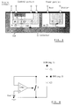
- FIG. 1 A common architecture of an integrated circuit comprising a power section and a control section is schematically depicted in Fig. 1.
- the power section is represented by a bipolar NPN power transistor having a vertical current flow, the collector of which coincides with an N-type substrate region 1 of the integrated circuit.
- the control section typically a logic circuitry, is realized within a P-type isolation region 2(P-well) diffused in the N-type substrate.
- Fig. 1 are symbolically shown the junction capacitance C1 between the substrate 1 and the isolation region 2, the other structural capacitances of the integrated architecture of the control circuitry, toward a common ground node, indicated as a whole with C2, as well as the NPN power transistor and the junction (diode) between the substrate 1 and the isolation region 2.
- FIG. 2 For an application of the type schematically represented in Fig. 1, the basic diagram of the device of the invention is shown in Fig. 2.
- the capacitance C1 represents the junction capacitance between the N-type substrate 1 (SUB) and the P-type isolation diffusion 2 (ISO).
- the capacitance C2 represents the series of capacitances relative to the junctions between regions of different type of conductivity that realize the integrated structures of the components of the control circuitry contained in the isolation region 2.
- the substrate 1 constitutes the collector of an NPN power transistor.
- the substrate-collector 1 (SUB) of the integrated circuit is at a positive voltage as referred to a common ground potential of the circuit, to which the emitter of the same NPN power transistor as well as the emitter of a generic NPN transistor of the control section of the integrated circuit may be coupled, as depicted in Figures 1 and 2.
- the isolation p-well region 2 (ISO) is connected, through a switch T to the ground node of the circuit.
- the comparator COMP maintains the switch T closed.
- the opening of the switch T places the isolation region 2 (ISO) in a floating or high-impedance condition with reference to the ground node so that the region potential is free to track the falling voltage of the substrate region 1, by assuming more and more negative voltage values, because of its capacitive coupling through C1 and C2.
- This dynamic potential tracking mechanism ensures that the isolation region 2 (ISO) remains always at a more negative potential than the potential assumed by the substrate region 1 (SUB).
- V2 The negative voltage value (V2) eventually reached by the isolation region 2 following a negative variation (negative dV/dt) of the voltage V1 of the substrate region 1, is tied to the relative values of the coupling capacitances C1 and C2 and to the value of an eventual leakage current.
- V 2 - C 1 C 1+ C 2 V 1
- the period of time during which the isolation region 2 remains at a negative voltage V2 dynamically reached because of its capacitive coupling is tied to the leakage current beside to the actual values of the coupling capacitances C1 and C2.
- such a period of time T must be sufficiently longer than the maximum interval of time during which the substrate region 1 may assume a negative (below-ground) voltage.
- Such a maximum period of time may be easily established in the design stage by knowing the electrical characteristics of the external load.
- the device of the invention will not require any externally connected additional component (for example capacitors to be connected in parallel to the intrinsic junction capacitances C1 and C2 of the integrated structure).
- the comparator Independently of the amplitude of the voltage swings toward negative values by part of the substrate region 1 (SUB) and, by dynamic capacitive voltage distribution by part of the region 2 (ISO) as well, as soon as the potential of the region 2 (ISO) by rising back again toward positive voltages, equals the threshold voltage V ref , which may be predefined so as to be lower than the conduction threshold of the junction between the regions 1 and 2, the comparator (COMP) switches thus closing again the switch T and re-establishing the clamping to ground potential of the region 2.
- Figures 3 and 4 show an application of the device of the invention in the case of an equivalent "dual" architecture of the integrated circuit, that is wherein the type of conductivities and polarities are all reversed.
- the logic of the comparator COMP will also be inverted so as to command the opening of the switch T following a positive dV/dt variation of the voltage of the substrate region 1 (which is normally negative).
- the basic electric scheme of the arrangement of the invention may be as shown in Fig. 5.
- the current generator I and the transistors T1 and T2 form an error amplifier, the voltage reference of which is placed to ground potential, while the switch (T in the scheme of Fig. 2) is implemented by the transistor T3.
- the node of region 2 Upon a negative dV/dt variation on the node of region 1, the node of region 2 assumes a potential that, in first approximation, is given by the equation (1), thus causing the saturation of the transistor T2 and therefore the turning off of the switch T3. In this way, the node coinciding with the region 2 presents an extremely high impedance.
- the potential of the region 2 rises again toward ground potential.
- the transistor T2 When it reaches ground potential, the transistor T2 exits saturation thus switching on again the switch T3 which re-establishes a connection of the region 2 to the ground node.
- circuit of Fig. 5 may be advantageously modified as shown in Fig. 6.
- the current absorption from the comparator is reduced by a number of times equivalent to the current gain of the stage T4 and, by virtue of the resistance R, the time necessary to effectively clamp the region 2 to ground potential may be considerably reduced because the transistor T3 is already biased when the potential of the region 2 tends to rise above ground potential (that is starts to be driven toward a positive voltage).
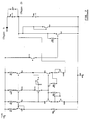
- FIG. 7 A complete circuit scheme of a device of the invention is depicted in Fig. 7.
- an error amplifier with emitter input and an output stage for driving the isolation region (2) node may be easily identified.
- Two diodes namely: Q93 and Q52, have been added in the circuit of the error amplifier in series with the emitters of the input transistors Q4 and Q5 in order to increase the maximum absolute voltage value that may be reached by the isolation region 2.
- the resistors in parallel to the base emitter junctions of the input pair of transistors Q4 and Q5 have the function of reducing the storage time thereof.
- the static biasing of Q5 has the function of preventing an excessively deep saturation thereof when conducting.
- the maximum operative voltage of the node coinciding with the region 1 (substrate-collector) and therefore the range of application of the device of the invention is a function of the amplitude of the gradient dV/dt, to which the same region 1 may be subject, of the capacitive voltage distribution that may be altered in the design stage by realizing capacitances in parallel to the intrinsic junction capacitances C1 and C2 (or by eventually connecting external capacitors), as well as of the open circuit collector emitter breakdown voltage (BVceo) of the integrated components.
- This last parameter will in fact determine the maximum value (modulus) that may be reached by the voltage of region 2.
- the BVceo of integrated transistors is of about 60V. Should the voltage of the region 2 reach the breakdown voltage of the components, a breakdown phenomenon would be triggered. Such a phenomenon, by injection of current from the ground node toward the region 2 according to equation (2), would reduce the time T with the risk of failing to ensure a junction isolation between the regions 1 and 2.
- other parameters that may critically affect the switching process of the invention may be suitably sized in the design stage by taking into account the above-mentioned limits.
Abstract
Description
- The present invention relates to a switching method for self-biasing regions of integrated circuits in order to ensure the maintenance of an effective junction isolation between two different regions coupled with each other also when one of the two regions is subject to large voltage swings and to a wholly integratable device implementing the method. The invention is particularly, though not exclusively, useful in integrated circuit that include power circuits and control circuits integrated on the same chip.
- In integrated circuits (IC), output power devices and logic control circuits are often integrated on the same chip. This kind of applications are innumerable: for example IC implementing a so-called "electronic transformer" for driving low-power halogen lamps, driving systems for displays, electric motors, actuators and the like.
- Considering an integrated power device, for example a bipolar transistor, a Darlington structure or an equivalent power MOS, having an external reactive load connected to the collector (or drain) node thereof, when the control circuitry switches off the power device, the collector's (or drain's) voltage may assume a negative value (below ground potential). These induced voltages may be extremely dangerous when the power device is integrated together with the control circuits on the same chip.
- A family of this type of devices is the one commonly known with the commercial name of VIPower. In these devices, as schematically shown in Fig. 1, the current terminal of an output power device, for example the collector of an NPN transistor, coincides with the substrate (region 1), commonly an N-type semiconductor, of the IC, while a logic control circuitry is integrated within an isolation region (region 2) commonly a P-type diffusion (e.g. a P-well), diffused in the
substrate region 1. - Isolation between the substrate-collector (region 1) and the isolation region (region 2) is ensured by the reverse bias of the P-N junction between the two regions.
- Under normal working conditions of the IC, the isolation region (P-well) containing control circuitry, is customarily connected to a certain reference voltage, which in a case as the one depicted in Fig 1, may be the lowest potential available, in practice to ground potential. In this type of architecture, during operation, the N-type substrate region which coincides with the output current terminal of the power device, in the example shown the collector of an NPN power transistor, is always at a positive voltage as referred to ground potential. Therefore the intrinsic parasitic transistors of the integrated structure are inhibited.
- If, for any reason, for example following the switching off of the power device, the N-type substrate region assumes a negative voltage (below-ground) of a negative value greater than the conduction threshold, the parasitic transistors of the integrated structure turn on and absorb current from the region containing the control circuitry. This may cause malfunctioning of the control circuits as well as of the controlled power devices.
- These risks could be easily eliminated by biasing the P-type isolation region (P-well) at a potential sufficiently more negative than the maximum negative voltage that may be reached by the N-type substrate region. However, negative bias voltage sources are not normally available and would need to be purposely implemented in the IC.
- For simplicity of description, in the ensuing description reference will be made almost exclusively to the sample case of an integrated architecture of the type depicted in Fig 1, based on a P-type isolation region, diffused in an N-type substrate. However it should be understood that similar considerations may be made for a "dual" situation of an architecture using inverted conductivity types and polarities. Moreover, it will be clear to the reader that the technical problems addressed by the present inventors may be encountered in a variety of other types of integrated circuits.
- In the past, there have been several proposals for preventing the occurrence of a direct biasing of the junction between two regions coupled together.
- French Patent Application No. 89/16144, filed on November 29, 1989, in the name of SGS-THOMSON MICROELECTRONICS and SIEMENS AUTOMOTIVE and US Patent No. 5,382,837, corresponding to the European patent application No. 91850287.8, filed on June 27, 1991, by the same applicant of the present application, describe circuit arrangements for ensuring junction isolation between two regions.
- Both these known proposed solutions propose to clamp a P-type isolation region to ground potential through a first switch as long as an N-type substrate region remains at a positive voltage and to connect the isolation region to the substrate region by a second switch when the latter region assumes a negative (below-ground) potential.
- These known solutions, beside requiring the use of two switches have critical aspects and drawbacks. A first disadvantage is represented by the need of ensuring with absolute reliability that the two switches may never be conductive simultaneously, because this would short-circuit the substrate region to ground. A second difficulty is in ensuring a timely biasing of the isolation region at the substrate potential when the substrate's voltage drops abruptly toward a negative (below-ground) potential.
- Therefore there is a need and/or utility for a simpler and more reliable switching or self-biasing method and device capable of ensuring a timely response in case of abrupt voltage changes of a first region, for example a substrate region, toward the voltage at which is normally biased a second region, for example an isolation region, in order to prevent any possibility of direct biasing the junction between the two regions.
- These objectives are fully met by the method and the device of the present invention.
- The method of the invention is based on maintaining the second region clamped at an available reference potential by a switch and commanding the opening of the switch, thus placing the region in a high impedance condition as referred to the node at said reference voltage to which is normally connected through the switch. The opening of the switch occurs automatically in response to a variation toward said reference potential of the voltage of the first region of a gradient sufficient to cause, by a capacitive dynamic voltage distribution, a momentary shift in the same direction of the voltage of the second region.
- In other words, the method implies the interruption of the connection of the second region to the clamp voltage node, thus allowing the second region to float and track, by virtue of its capacitive coupling the voltage swing of the first region, which is subject to abrupt voltage changes toward said clamp voltage.
- By effect of the capacitive coupling and therefore of a dynamic voltage distribution, when an abrupt voltage variation of the first region toward the reference potential to which the second region is clamped occurs the second region is momentarily subject to a voltage shift from the clamping reference voltage of the node to which is connected through the switch in the same direction of the variation (dV/dt) of the voltage of the first region; thus the second region assumes momentarily a potential lower (or greater in a dual situation with inverted polarities) then the reference voltage to which is clamped. This momentary shift eventually causes the opening of the switch and thus permits to the potential of the second region to continue to track (in a floating state) the voltage change (dV/dt) of the first region by virtue of the capacitive coupling existing therebetween, thus making impossible the occurrence of a direct biasing of the junction between the two regions.
- Of course, the system is capable of reacting in the above-described manner, only in presence of a gradient of variation of the voltage of the first region (dV/dt) of a sufficient magnitude. On the other hand, in systems operating in a switching mode, the changes of state are typically step-functions (that is extremely abrupt) and therefore the magnitude of the gradient of the voltage variation is generally sufficient.
- In practice, the dynamic self-biasing switching device of the invention may consist of a single integrated switch capable of establishing a connection of the second region with a node at a reference voltage and a controlling comparator.
- The different aspects and advantages of the invention will become even more evident through the following description of several important embodiments, included herein for purely illustrative and non limitative purposes, and by referring to the annexed drawings, wherein:
- Figure 1 shows the architecture of an integrated circuit for single supply wherein the above-identified technical problems may be encountered;
- Figure 2 is a diagram of the device of the invention;
- Figures 3 and 4 show a dual situation of the one depicted in Figures 1 and 2;
- Figure 5 is a basic circuit diagram of an embodiment of the invention;
- Figure 6 is a basic circuit diagram according to an alternative embodiment of the invention;
- Figure 7 is a complete circuit diagram of a device of the invention;
- Figure 8 shows circuit's voltage signals obtained by simulation.
- A common architecture of an integrated circuit comprising a power section and a control section is schematically depicted in Fig. 1. In the example shown, the power section is represented by a bipolar NPN power transistor having a vertical current flow, the collector of which coincides with an N-
type substrate region 1 of the integrated circuit. - The control section, typically a logic circuitry, is realized within a P-type isolation region 2(P-well) diffused in the N-type substrate. In Fig. 1 are symbolically shown the junction capacitance C1 between the
substrate 1 and theisolation region 2, the other structural capacitances of the integrated architecture of the control circuitry, toward a common ground node, indicated as a whole with C2, as well as the NPN power transistor and the junction (diode) between thesubstrate 1 and theisolation region 2. - For an application of the type schematically represented in Fig. 1, the basic diagram of the device of the invention is shown in Fig. 2.
- The capacitance C1 represents the junction capacitance between the N-type substrate 1 (SUB) and the P-type isolation diffusion 2 (ISO). The capacitance C2 represents the series of capacitances relative to the junctions between regions of different type of conductivity that realize the integrated structures of the components of the control circuitry contained in the
isolation region 2. - In the examples of Figures 1 and 2, the
substrate 1 constitutes the collector of an NPN power transistor. During normal operation, the substrate-collector 1 (SUB) of the integrated circuit is at a positive voltage as referred to a common ground potential of the circuit, to which the emitter of the same NPN power transistor as well as the emitter of a generic NPN transistor of the control section of the integrated circuit may be coupled, as depicted in Figures 1 and 2. - According to the basic scheme of Fig. 2, the isolation p-well region 2 (ISO) is connected, through a switch T to the ground node of the circuit.
- As long as the potential of the
region 2 coincides with the ground potential, the comparator COMP maintains the switch T closed. - When for any reason, as for example because of the switching off of the output power transistor and in presence of an inductive external load, the potential of the region 1 (SUB) drops abruptly toward ground potential (being trendily dragged inertially toward negative voltage values), by capacitive coupling also the potential of the isolation region 2 (ISO) is momentarily dragged toward negative (below-ground) voltage values. Such a dynamic potential shifting of the
isolation region 2 beyond the reference voltage (ground potential) to which is clamped by the switch T, in the example shown toward a negative voltage, is detected by the comparator COMP which changes state thus opening the switch T. - The opening of the switch T places the isolation region 2 (ISO) in a floating or high-impedance condition with reference to the ground node so that the region potential is free to track the falling voltage of the
substrate region 1, by assuming more and more negative voltage values, because of its capacitive coupling through C1 and C2. This dynamic potential tracking mechanism ensures that the isolation region 2 (ISO) remains always at a more negative potential than the potential assumed by the substrate region 1 (SUB). - The negative voltage value (V2) eventually reached by the
isolation region 2 following a negative variation (negative dV/dt) of the voltage V1 of thesubstrate region 1, is tied to the relative values of the coupling capacitances C1 and C2 and to the value of an eventual leakage current. - By neglecting any leakage current, the following relationship holds:

- On the other hand, the period of time during which the
isolation region 2 remains at a negative voltage V2 dynamically reached because of its capacitive coupling is tied to the leakage current beside to the actual values of the coupling capacitances C1 and C2. By supposing a leakage current i of a constant value, such a period of time may be calculated with the following equation:
- Of course, such a period of time T must be sufficiently longer than the maximum interval of time during which the
substrate region 1 may assume a negative (below-ground) voltage. Such a maximum period of time may be easily established in the design stage by knowing the electrical characteristics of the external load. - It may be easily verified that, in the majority of cases, the levels of leakage current are sufficiently low so as to make the junction capacitances C1 and C2 of the
region 2 quite appropriate for the purpose. The need of increasing the values of the coupling capacitances, by eventually integrating parallel capacitances could present itself only in case the level of leakage currents would be so high as to make the "hold" time T too short. - In practice, in the majority of cases, the device of the invention will not require any externally connected additional component (for example capacitors to be connected in parallel to the intrinsic junction capacitances C1 and C2 of the integrated structure).
- Independently of the amplitude of the voltage swings toward negative values by part of the substrate region 1 (SUB) and, by dynamic capacitive voltage distribution by part of the region 2 (ISO) as well, as soon as the potential of the region 2 (ISO) by rising back again toward positive voltages, equals the threshold voltage Vref, which may be predefined so as to be lower than the conduction threshold of the junction between the
regions region 2. - Figures 3 and 4 show an application of the device of the invention in the case of an equivalent "dual" architecture of the integrated circuit, that is wherein the type of conductivities and polarities are all reversed. Of course, in such an alternative embodiment, the logic of the comparator COMP will also be inverted so as to command the opening of the switch T following a positive dV/dt variation of the voltage of the substrate region 1 (which is normally negative).
- For the case of Figures 1 and 2, the basic electric scheme of the arrangement of the invention may be as shown in Fig. 5. The current generator I and the transistors T1 and T2, form an error amplifier, the voltage reference of which is placed to ground potential, while the switch (T in the scheme of Fig. 2) is implemented by the transistor T3.
- Upon a negative dV/dt variation on the node of
region 1, the node ofregion 2 assumes a potential that, in first approximation, is given by the equation (1), thus causing the saturation of the transistor T2 and therefore the turning off of the switch T3. In this way, the node coinciding with theregion 2 presents an extremely high impedance. At the end of a period of time T given, in first approximation, by the equation (2) or upon a positive dV/dt variation of the voltage of theregion 1, the potential of theregion 2 rises again toward ground potential. - When it reaches ground potential, the transistor T2 exits saturation thus switching on again the switch T3 which re-establishes a connection of the
region 2 to the ground node. - In order to avoid overloading the output of the comparator and therefore obtaining an improved switching performance, the circuit of Fig. 5 may be advantageously modified as shown in Fig. 6.
- By adding a stage formed by the transistor T4, the current absorption from the comparator is reduced by a number of times equivalent to the current gain of the stage T4 and, by virtue of the resistance R, the time necessary to effectively clamp the
region 2 to ground potential may be considerably reduced because the transistor T3 is already biased when the potential of theregion 2 tends to rise above ground potential (that is starts to be driven toward a positive voltage). - A complete circuit scheme of a device of the invention is depicted in Fig. 7.
- As can be noted from the scheme, an error amplifier with emitter input and an output stage for driving the isolation region (2) node may be easily identified.
- Two diodes, namely: Q93 and Q52, have been added in the circuit of the error amplifier in series with the emitters of the input transistors Q4 and Q5 in order to increase the maximum absolute voltage value that may be reached by the
isolation region 2. The resistors in parallel to the base emitter junctions of the input pair of transistors Q4 and Q5 have the function of reducing the storage time thereof. - Finally, the static biasing of Q5 has the function of preventing an excessively deep saturation thereof when conducting.
- Voltage diagrams of the node coinciding with a
substrate region 1, and of the node coinciding with anisolation region 2, obtained by simulating the use of a switching circuit as the one depicted in Fig. 7 are shown in Fig. 8. - The simulations have fully confirmed the effectiveness of the device of the invention. From the simulations, it has been found that the maximum operative voltage of the node coinciding with the region 1 (substrate-collector) and therefore the range of application of the device of the invention is a function of the amplitude of the gradient dV/dt, to which the
same region 1 may be subject, of the capacitive voltage distribution that may be altered in the design stage by realizing capacitances in parallel to the intrinsic junction capacitances C1 and C2 (or by eventually connecting external capacitors), as well as of the open circuit collector emitter breakdown voltage (BVceo) of the integrated components. This last parameter will in fact determine the maximum value (modulus) that may be reached by the voltage ofregion 2. - According to common fabrication processes of this type of devices, the BVceo of integrated transistors is of about 60V. Should the voltage of the
region 2 reach the breakdown voltage of the components, a breakdown phenomenon would be triggered. Such a phenomenon, by injection of current from the ground node toward theregion 2 according to equation (2), would reduce the time T with the risk of failing to ensure a junction isolation between theregions
Claims (8)
- A method of dynamically biasing a second region (2) of a first type of conductivity, normally clamped at a reference potential, contained within a first region (1) of a second type of conductivity whose potential (V1) is subject to changes, in order to maintain a reverse bias on the junction between said regions (1, 2) even when the potential (V1) of said first region (1) undergoes an abrupt change toward said reference potential that could eventually lead to directly bias said junction, which comprisesclamping said second region (2) to said reference potential through at least a switch (T);opening said switch (T) thus placing said second region (2) in a high impedance condition as referred to the node at said reference potential in response to a variation toward said reference potential of the potential (V1) of said first region (1) sufficient to cause, by dynamic capacitive voltage distribution, a voltage shift of the potential (V2) of said second region in the same direction;closing again said switch (T) upon a discharge of said second region (2) from the potential assumed by said capacitive coupling caused by a leakage current toward the node at said reference potential or in response of a variation in an opposite direction of the potential (V1) of said first region (1) sufficient to cause, by dynamic capacitive voltage distribution a return of the potential (V2) of said second region (2) to said reference potential.
- The method according to claim 1, wherein said first region (1) is an N-type substrate region and said second region (2) is a P-type isolation region.
- The method according to claim 1, wherein said reference potential is a common ground node potential.
- The method according to claim 3, wherein the opening of said switch (T) is commanded upon the dropping of the potential (V2) of said second region (2) below a positive threshold voltage (Vref) referred to ground potential.
- The method according to claim 1, wherein said regions (1, 2) are regions of an integrated circuit comprising at least an integrated vertical type power device which employs said first region (1) as an output current terminal and which comprises at least a logic control circuitry contained in said second region (2).
- A device for dynamically biasing a second region (2) of a first type of conductivity of an integrated circuit which is normally biased at a reference voltage and is contained in a first region (1) of a second type of conductivity, which constitutes an output current node of at least a power device, characterized by comprisingan integrated switch (T) connecting said second region (2) to a node at said reference voltage;a comparator (COMP) for opening said switch (T) thus placing said second region (2) in a high impedance condition as referred to said reference voltage node, in response to a variation toward said reference voltage of the voltage (1) of said first region (1) sufficient to cause, by dynamic capacitive voltage distribution, a shift in the same direction of the potential (V2) of said second region (2) from said reference voltage.
- The device according to claim 6, wherein the change of state of said comparator (COMP) occurs upon the crossing in a direction or in the opposite direction of a threshold voltage (Vref) as referred to said reference voltage.
- The device according to claim 6, wherein said first region (1) is an N-type substrate region and said second region (2) is an isolation P-type region, diffused in said substrate region (1) and said switch (T) is opened by said comparator (COMP) upon a variation of the voltage (V1) of said first substrate region (1) from a positive value toward a negative (below-ground) value.
Priority Applications (4)
| Application Number | Priority Date | Filing Date | Title |
|---|---|---|---|
| DE69518064T DE69518064T2 (en) | 1995-03-22 | 1995-03-22 | Method and arrangement for dynamic automatic biasing of areas in integrated circuits |
| EP95830109A EP0734070B1 (en) | 1995-03-22 | 1995-03-22 | Method and device for dynamically self-biasing regions of integrated circuits |
| US08/619,421 US5804866A (en) | 1995-03-22 | 1996-03-21 | Method and device for dynamically self-biasing regions of integrated circuits |
| JP8093444A JPH08306794A (en) | 1995-03-22 | 1996-03-22 | Method and equipment for dynamic self-bias region of integrated circuit |
Applications Claiming Priority (1)
| Application Number | Priority Date | Filing Date | Title |
|---|---|---|---|
| EP95830109A EP0734070B1 (en) | 1995-03-22 | 1995-03-22 | Method and device for dynamically self-biasing regions of integrated circuits |
Publications (2)
| Publication Number | Publication Date |
|---|---|
| EP0734070A1 true EP0734070A1 (en) | 1996-09-25 |
| EP0734070B1 EP0734070B1 (en) | 2000-07-19 |
Family
ID=8221876
Family Applications (1)
| Application Number | Title | Priority Date | Filing Date |
|---|---|---|---|
| EP95830109A Expired - Lifetime EP0734070B1 (en) | 1995-03-22 | 1995-03-22 | Method and device for dynamically self-biasing regions of integrated circuits |
Country Status (4)
| Country | Link |
|---|---|
| US (1) | US5804866A (en) |
| EP (1) | EP0734070B1 (en) |
| JP (1) | JPH08306794A (en) |
| DE (1) | DE69518064T2 (en) |
Cited By (3)
| Publication number | Priority date | Publication date | Assignee | Title |
|---|---|---|---|---|
| EP0836230A2 (en) * | 1996-10-14 | 1998-04-15 | Sharp Kabushiki Kaisha | Power transistor |
| EP1028468A1 (en) * | 1999-02-09 | 2000-08-16 | STMicroelectronics S.r.l. | Biasing circuit for isolation region in integrated power circuit |
| EP1309011A2 (en) * | 2001-10-31 | 2003-05-07 | Motorola, Inc. | Semiconductor component and method of operation |
Families Citing this family (4)
| Publication number | Priority date | Publication date | Assignee | Title |
|---|---|---|---|---|
| US7081776B2 (en) * | 2003-02-24 | 2006-07-25 | Spansion Llc | Voltage detection circuit, semiconductor device, method for controlling voltage detection circuit |
| US9142951B2 (en) | 2009-07-28 | 2015-09-22 | Stmicroelectronics (Rousset) Sas | Electronic device for protecting against a polarity reversal of a DC power supply voltage, and its application to motor vehicles |
| FR2948828B1 (en) * | 2009-07-28 | 2011-09-30 | St Microelectronics Rousset | ELECTRONIC DEVICE FOR PROTECTION AGAINST A POLARITY INVERSION OF A CONTINUOUS POWER SUPPLY VOLTAGE, AND APPLICATION TO THE AUTOMOTIVE DOMAIN |
| FR3083919A1 (en) * | 2018-07-13 | 2020-01-17 | Stmicroelectronics (Rousset) Sas | PROTECTED ELECTRONIC CHIP |
Citations (2)
| Publication number | Priority date | Publication date | Assignee | Title |
|---|---|---|---|---|
| JPH01212463A (en) * | 1988-02-19 | 1989-08-25 | Mitsubishi Electric Corp | Semiconductor integrated circuit device |
| EP0432058A1 (en) * | 1989-11-29 | 1991-06-12 | STMicroelectronics S.A. | Dynamic isolation circuit for integrated circuits |
Family Cites Families (1)
| Publication number | Priority date | Publication date | Assignee | Title |
|---|---|---|---|---|
| US5065055A (en) * | 1990-12-20 | 1991-11-12 | Sun Microsystems, Inc. | Method and apparatus for high-speed bi-CMOS differential amplifier with controlled output voltage swing |
-
1995
- 1995-03-22 DE DE69518064T patent/DE69518064T2/en not_active Expired - Fee Related
- 1995-03-22 EP EP95830109A patent/EP0734070B1/en not_active Expired - Lifetime
-
1996
- 1996-03-21 US US08/619,421 patent/US5804866A/en not_active Expired - Lifetime
- 1996-03-22 JP JP8093444A patent/JPH08306794A/en not_active Withdrawn
Patent Citations (2)
| Publication number | Priority date | Publication date | Assignee | Title |
|---|---|---|---|---|
| JPH01212463A (en) * | 1988-02-19 | 1989-08-25 | Mitsubishi Electric Corp | Semiconductor integrated circuit device |
| EP0432058A1 (en) * | 1989-11-29 | 1991-06-12 | STMicroelectronics S.A. | Dynamic isolation circuit for integrated circuits |
Non-Patent Citations (1)
| Title |
|---|
| PATENT ABSTRACTS OF JAPAN vol. 013, no. 522 (E - 849) 21 November 1989 (1989-11-21) * |
Cited By (6)
| Publication number | Priority date | Publication date | Assignee | Title |
|---|---|---|---|---|
| EP0836230A2 (en) * | 1996-10-14 | 1998-04-15 | Sharp Kabushiki Kaisha | Power transistor |
| EP0836230A3 (en) * | 1996-10-14 | 1998-08-05 | Sharp Kabushiki Kaisha | Power transistor |
| EP1028468A1 (en) * | 1999-02-09 | 2000-08-16 | STMicroelectronics S.r.l. | Biasing circuit for isolation region in integrated power circuit |
| US6815779B1 (en) | 1999-02-09 | 2004-11-09 | Stmicroelectronics S.R.L. | Integrated circuit including protection against polarity inversion of the substrate potential |
| EP1309011A2 (en) * | 2001-10-31 | 2003-05-07 | Motorola, Inc. | Semiconductor component and method of operation |
| EP1309011A3 (en) * | 2001-10-31 | 2008-07-02 | Freescale Semiconductor, Inc. | Semiconductor component and method of operation |
Also Published As
| Publication number | Publication date |
|---|---|
| DE69518064T2 (en) | 2000-12-21 |
| EP0734070B1 (en) | 2000-07-19 |
| US5804866A (en) | 1998-09-08 |
| JPH08306794A (en) | 1996-11-22 |
| DE69518064D1 (en) | 2000-08-24 |
Similar Documents
| Publication | Publication Date | Title |
|---|---|---|
| EP0090665A2 (en) | Semiconductor memory device | |
| CN103733336A (en) | Combination ESD protection circuits and methods | |
| CN101174622B (en) | Electrostatic discharge protecting equipment of connection pad and its method and structure | |
| CA1101565A (en) | Semiconductor switch | |
| US6248616B1 (en) | Method for suppressing parasitic effects in a junction-isolation integrated circuit | |
| EP0734070B1 (en) | Method and device for dynamically self-biasing regions of integrated circuits | |
| JPS61169018A (en) | Switching circuit for damping vibration | |
| JPS6271257A (en) | Protecting circuit for induction load switch transistor | |
| EP0042581B1 (en) | Integrated circuit | |
| US4893212A (en) | Protection of power integrated circuits against load voltage surges | |
| US4599631A (en) | Semiconductor apparatus having a zener diode integral with a resistor-transistor combination | |
| WO1985004524A1 (en) | Integrated circuit and method for biasing an epitaxial layer | |
| US6108181A (en) | Electrostatic discharge (ESD) circuit | |
| US5608259A (en) | Reverse current flow prevention in a diffused resistor | |
| EP0084000A2 (en) | CMOS device | |
| US5075577A (en) | Tristate output circuit with input protection | |
| JPH0831945A (en) | Integrated power semiconductor device | |
| JP3179630B2 (en) | Epitaxial tub bias structure and integrated circuit | |
| WO2000035017A1 (en) | Analogue switch | |
| US4096400A (en) | Inductive load driving amplifier | |
| EP0715409A1 (en) | Circuit for limiting the output voltage of a power transistor | |
| US6624502B2 (en) | Method and device for limiting the substrate potential in junction isolated integrated circuits | |
| US6815779B1 (en) | Integrated circuit including protection against polarity inversion of the substrate potential | |
| EP0730299B1 (en) | Circuit for biasing epitaxial regions | |
| JP2917403B2 (en) | Motor drive circuit |
Legal Events
| Date | Code | Title | Description |
|---|---|---|---|
| PUAI | Public reference made under article 153(3) epc to a published international application that has entered the european phase |
Free format text: ORIGINAL CODE: 0009012 |
|
| AK | Designated contracting states |
Kind code of ref document: A1 Designated state(s): DE FR GB IT |
|
| 17P | Request for examination filed |
Effective date: 19970313 |
|
| GRAG | Despatch of communication of intention to grant |
Free format text: ORIGINAL CODE: EPIDOS AGRA |
|
| 17Q | First examination report despatched |
Effective date: 19990519 |
|
| GRAG | Despatch of communication of intention to grant |
Free format text: ORIGINAL CODE: EPIDOS AGRA |
|
| GRAH | Despatch of communication of intention to grant a patent |
Free format text: ORIGINAL CODE: EPIDOS IGRA |
|
| GRAH | Despatch of communication of intention to grant a patent |
Free format text: ORIGINAL CODE: EPIDOS IGRA |
|
| GRAA | (expected) grant |
Free format text: ORIGINAL CODE: 0009210 |
|
| AK | Designated contracting states |
Kind code of ref document: B1 Designated state(s): DE FR GB IT |
|
| REF | Corresponds to: |
Ref document number: 69518064 Country of ref document: DE Date of ref document: 20000824 |
|
| ITF | It: translation for a ep patent filed |
Owner name: SOCIETA' ITALIANA BREVETTI S.P.A. |
|
| ET | Fr: translation filed | ||
| PLBE | No opposition filed within time limit |
Free format text: ORIGINAL CODE: 0009261 |
|
| STAA | Information on the status of an ep patent application or granted ep patent |
Free format text: STATUS: NO OPPOSITION FILED WITHIN TIME LIMIT |
|
| 26N | No opposition filed | ||
| REG | Reference to a national code |
Ref country code: GB Ref legal event code: IF02 |
|
| PGFP | Annual fee paid to national office [announced via postgrant information from national office to epo] |
Ref country code: DE Payment date: 20040401 Year of fee payment: 10 |
|
| PG25 | Lapsed in a contracting state [announced via postgrant information from national office to epo] |
Ref country code: IT Free format text: LAPSE BECAUSE OF NON-PAYMENT OF DUE FEES;WARNING: LAPSES OF ITALIAN PATENTS WITH EFFECTIVE DATE BEFORE 2007 MAY HAVE OCCURRED AT ANY TIME BEFORE 2007. THE CORRECT EFFECTIVE DATE MAY BE DIFFERENT FROM THE ONE RECORDED. Effective date: 20050322 |
|
| PG25 | Lapsed in a contracting state [announced via postgrant information from national office to epo] |
Ref country code: DE Free format text: LAPSE BECAUSE OF NON-PAYMENT OF DUE FEES Effective date: 20051001 |
|
| PGFP | Annual fee paid to national office [announced via postgrant information from national office to epo] |
Ref country code: GB Payment date: 20060223 Year of fee payment: 12 |
|
| GBPC | Gb: european patent ceased through non-payment of renewal fee |
Effective date: 20070322 |
|
| PG25 | Lapsed in a contracting state [announced via postgrant information from national office to epo] |
Ref country code: GB Free format text: LAPSE BECAUSE OF NON-PAYMENT OF DUE FEES Effective date: 20070322 |
|
| PGFP | Annual fee paid to national office [announced via postgrant information from national office to epo] |
Ref country code: FR Payment date: 20070227 Year of fee payment: 13 |
|
| REG | Reference to a national code |
Ref country code: FR Ref legal event code: ST Effective date: 20081125 |
|
| PG25 | Lapsed in a contracting state [announced via postgrant information from national office to epo] |
Ref country code: FR Free format text: LAPSE BECAUSE OF NON-PAYMENT OF DUE FEES Effective date: 20080331 |