EP0732823A2 - Method for clock recovery of a digital signal on the reception side - Google Patents
Method for clock recovery of a digital signal on the reception side Download PDFInfo
- Publication number
- EP0732823A2 EP0732823A2 EP95117909A EP95117909A EP0732823A2 EP 0732823 A2 EP0732823 A2 EP 0732823A2 EP 95117909 A EP95117909 A EP 95117909A EP 95117909 A EP95117909 A EP 95117909A EP 0732823 A2 EP0732823 A2 EP 0732823A2
- Authority
- EP
- European Patent Office
- Prior art keywords
- clock
- fifo memory
- fill level
- digital signals
- signal
- Prior art date
- Legal status (The legal status is an assumption and is not a legal conclusion. Google has not performed a legal analysis and makes no representation as to the accuracy of the status listed.)
- Granted
Links
- 238000000034 method Methods 0.000 title claims abstract description 29
- 238000011084 recovery Methods 0.000 title claims description 7
- 230000005540 biological transmission Effects 0.000 claims abstract description 12
- 230000006870 function Effects 0.000 claims description 4
- 230000002123 temporal effect Effects 0.000 claims description 2
- 238000012935 Averaging Methods 0.000 description 6
- 238000010586 diagram Methods 0.000 description 2
- 238000009499 grossing Methods 0.000 description 2
- 230000015572 biosynthetic process Effects 0.000 description 1
- 230000022131 cell cycle Effects 0.000 description 1
- 230000001419 dependent effect Effects 0.000 description 1
- 230000007257 malfunction Effects 0.000 description 1
- 230000005236 sound signal Effects 0.000 description 1
- 230000001360 synchronised effect Effects 0.000 description 1
- 230000001960 triggered effect Effects 0.000 description 1
Images

Classifications
-
- H—ELECTRICITY
- H04—ELECTRIC COMMUNICATION TECHNIQUE
- H04J—MULTIPLEX COMMUNICATION
- H04J3/00—Time-division multiplex systems
- H04J3/02—Details
- H04J3/06—Synchronising arrangements
- H04J3/062—Synchronisation of signals having the same nominal but fluctuating bit rates, e.g. using buffers
- H04J3/0632—Synchronisation of packets and cells, e.g. transmission of voice via a packet network, circuit emulation service [CES]
-
- H—ELECTRICITY
- H04—ELECTRIC COMMUNICATION TECHNIQUE
- H04L—TRANSMISSION OF DIGITAL INFORMATION, e.g. TELEGRAPHIC COMMUNICATION
- H04L12/00—Data switching networks
- H04L12/54—Store-and-forward switching systems
- H04L12/56—Packet switching systems
- H04L12/5601—Transfer mode dependent, e.g. ATM
- H04L2012/5614—User Network Interface
- H04L2012/5616—Terminal equipment, e.g. codecs, synch.
-
- H—ELECTRICITY
- H04—ELECTRIC COMMUNICATION TECHNIQUE
- H04L—TRANSMISSION OF DIGITAL INFORMATION, e.g. TELEGRAPHIC COMMUNICATION
- H04L12/00—Data switching networks
- H04L12/54—Store-and-forward switching systems
- H04L12/56—Packet switching systems
- H04L12/5601—Transfer mode dependent, e.g. ATM
- H04L2012/5672—Multiplexing, e.g. coding, scrambling
- H04L2012/5674—Synchronisation, timing recovery or alignment
Definitions
- the invention relates to a method for receiving clock recovery for digital signals with a constant bit rate after cell-structured, asynchronous transmission with pauses of different lengths between individual cells using the fill level of a FIFO memory, in which the received digital signals are written.
- the transmission of digital signals is often asynchronous and cell-structured, whereupon the digital signals on the receiving side have to be formed into a continuous digital signal with a constant bit rate. This requires the recovery of the clock on which the digital signals are based - also referred to below as the data clock.
- a method for cell-structured asynchronous transmission of digital signals is described, for example, in Martin Prycker et al .: "ASYNCHRONOUS TRANSFER MODE, Solution for Broadband ISDN", Verlag Ellis Horwood, pages 97 to 116, the abbreviation ATM being introduced for this method.
- the preferred application of the method is the transmission of broadband signals.
- a continuous data stream can be recovered by temporarily storing the data in a FIFO memory and then deriving the clock from the fill level of this FIFO memory.
- a problem that has not yet been solved satisfactorily is jitter-free clock recovery, which causes difficulties due to the cell structure of the signal with pauses of different lengths between the individual cells.
- the object of the invention is to provide a method for recovering a continuous, largely jitter-free clock.
- This object is achieved in that at the beginning of a transmission in the FIFO memory comprising several cells of the received signals, the digital signals are first read in with a received clock until the FIFO memory is half full, that the ones written into the FIFO memory Digital signals are read out with a readout clock, the frequency of which is lower than the frequency of the received clock, and that a signal for controlling the frequency of the readout clock is derived from the respective fill level of the FIFO memory during the readout.
- the method according to the invention has the advantage that only a larger FIFO memory is required on the receiving end in the terminal adapter in order to buffer the data. There is also the possibility of arranging this FIFO memory in front of a cell resolver, so that the cell resolver has to be operated with the lower data clock frequency and not with the substantially higher network clock frequency.
- the method according to the invention can advantageously be used in the transmission of digital signals, for example in the transmission of coded audio and video signals, including MPEG-coded signals.
- the known MPEG methods allow the selection of different transmission bit rates depending on the desired quality of the decoded analog signal.
- the exploitation of these properties of the encoders and decoders make clock recovery necessary, which allows the recovery of the clock of the MPEG signal, which is constant per se, at the receiving end.
- the encoders and decoders can be set to different bit rates, but the bit rate remains constant during operation.
- the manipulated variable is supplied to several voltage-controlled oscillators. This makes it possible to cover a large frequency range.
- An advantageous embodiment of the method according to the invention is that the fill level of the FIFO memory is queried at larger time intervals. As a result, a rough smoothing of the data clock is already possible. It is preferably provided in the method according to the invention that a cell clock obtained from the received digital signals is used for the temporal determination of queries regarding the fill level of the FIFO memory.
- a further smoothing of the data clock is possible by averaging over several queries of the fill level of the FIFO memory.
- a simple possibility for selecting the data clock is that a controllable frequency divider is connected downstream of the voltage-controlled oscillator in order to obtain the data clock with a selectable frequency.
- the frequency divider can be controlled by manual inputs and / or an internal clock can be derived from the signal of the voltage-controlled oscillator.
- An automatic setting is possible, for example, in that the frequency divider can be controlled as a function of control data received with the digital signals or as a function of the fill level.
- Another arrangement for carrying out the method according to the invention is that the FIFO memory is arranged in front of a cell resolver.
- This has the advantage that circuits following the FIFO memory, in particular the cell resolver, a bit deinterleaving and a parity decoder, can be operated at a lower frequency.
- a terminal adapter with such circuits which is suitable for the application of the method and the arrangement according to the invention, is described by Ulf Aßmus and Serafin Nunes in "Transmission of Coded Audio Signals of Low Bit Rate in a Future ATM Network", RTM Issue 3, 1994 , Pp. 85 to 91.
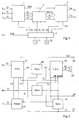
- the inputs 5, 6, 7, 8 together with the received data Di are a clock signal Ti, the maximum the frequency of the network clock can have a reset signal R and a signal CSt, which indicates the beginning of a cell of the supplied digital signals and is therefore called cell start signal in the following.
- the supplied digital signals as an internal data stream Dint, the respective fill level of the FIFO memory contained in the memory 1 as an n-bit signal Zn and a reset signal R can be taken from the memory 1.
- the memory 1 will be described later in connection with FIG. 2.
- the mean value M (Zn) is formed from a plurality of values of the fill level Zn in the mean value generator 2 and is fed together with a reset signal R to the clock generator 3, at the output of which the data Do are present in a constant and continuous data cycle To.
- the clock center 4 has two input devices 11, 12, with which quantities i and k can be entered manually.
- i means the distance between two values of the fill level Zn taken over for averaging, derived from the cell cycle.
- the cell start signal CSt is counted in the clock center 4 until the set value of i is reached, whereupon a clock signal T5 is generated.
- K values are used for averaging, for which k can be set with the aid of the input device 12.
- Fig. 2 shows the memory 1 (Fig. 1) in more detail.
- the received digital signals are fed from the input 5 to the data input of a FIFO memory 21, into which the digital signals Di are written with the clock Ti supplied at 6.
- the clock Ti is also fed to a synchronizing circuit 22, which will be described in detail later.
- the reset signal R passes from the input 7 to a reset circuit 23 which also contains the signals FE and FF from the FIFO memory 21 when the FIFO memory is empty or full. Furthermore, the reset circuit 23 passes the signal R to the FIFO memory 21 and on to a further synchronization circuit 24.
- a counter 25 is connected via a third synchronization circuit 26 to an output of the FIFO memory 21, which outputs a signal HF (half full).
- the content of the counter which is designed as an up / down counter, reflects the fill level of the FIFO memory 21 and thus represents a pointer to the fill level.
- the counter 25 receives, in addition to a reset pulse R, the clock signals Tl and Ts, which decrement the fill level during a read operation and increment the fill level during a write operation.
- the clock signal T1 is supplied to the circuit shown in FIG. 2 by the clock center 4 via an input 27.
- the reset signal R can be extracted for further circuits via an output 28.
- a third output 29 carries the fill level Zn, while the data Dint is forwarded to the clock generator 3 by an output 30.
- the clocks T1 and Ti are not synchronous with one another, signals which are initially in the time pattern of the clock Ti are brought into the time pattern of the clock T1 by the synchronizing circuits 22, 24, 26.
- the signal HF which characterizes half the fill level, is in the grid of the clock Ti.
- the counter 25 is operated in the grid of the clock T1. Therefore, a pulse FH * is derived in the synchronization circuit 26, which coincides in time with the first pulse of the clock signal T1, which occurs after a pulse HF.
- a D flip-flop can be triggered in a simple manner with the clock T1, the data input of which is supplied with the pulse HF.
- the synchronization circuit 24 only releases the clock signal TL after switching on or a reset when the pulse FH * indicates that half the fill level has been reached. Then, using the clock TL, the reading of the data from the FIFO memory 21 and a corresponding decrementing of the counter reading begins.
- the incrementation is carried out in each case by a pulse of the clock Ts, which is derived from the clock Ti with the aid of the synchronization circuit 22 and is converted into the grid of the clock T1 via the clock T1. This is done in such a way that it is ensured that the counter does not receive pulses for incrementing and decrementing at the same time.
- the counter 25 is set to half the count each time the FIFO memory 21 emits a pulse HF. In the event that - due to a malfunction - the FIFO memory is either full or empty, a reset is initiated via the FF or FE pulses, whereby the original state is restored when the device is switched on.
- the number of bits that can be removed from output 29 depends on the size of the FIFO memory, which is given with 2 n bits.
- the pointer can be obtained from the counter readings of the counters required for the FIFO memory for reading in and reading out.
- the averager 2 (FIG. 1) is shown in more detail in FIG. 3.
- the fill level Zn is fed from the memory 1 (FIG. 1) to an input 33.
- a value of Zn is accepted as a n-bit word in a read-write memory 35.
- Zn values are saved as required in individual cases for the subsequent averaging.
- the number k to be selected and set at 12 (FIG. 1) is fed to the read-write memory 35 by a counter 36, which counts upwards starting with a reset pulse R supplied at 37 until the clock signal T2 arrives, and thereby the number k reached.
- the actual averaging takes place with the aid of an adder 38, a register 39 and a divider 40.
- the adders 38, the register 39 and the divider 40 reset.
- Each of the data words arriving there is added in the adder 38 to the sum of (k-1) values of the preceding data words, the oldest value of k values always being replaced by the current, latest value.
- the sum 1 to k is then written into register 39 and is available for addition with the following data word.
- the sum added up for k data words is then divided in the divider by k, at whose output 41 the mean value M (Zn) from k words is present.
- the register 39 is driven by a clock T3 and the divider by a clock T4.
- the clock signals T2 to T4 are supplied from the clock center 4 (FIG. 1).
- the k-fold addition creates an n + k bit-wide data stream. If k is selected as a multiple of two, the division in the divider 40 can be carried out in a simple manner by shifting in a shift register as a modulo-2 division.
- Average values M (Zn) at 45 are fed to the clock generator 3 (FIG. 1) shown in FIG. 4. These are converted into an analog signal in a digital / analog converter 46 and then low-pass filtered at 47.
- the output signal of the low-pass filter 47 represents a manipulated variable for one Controllable oscillator 48, which generates a frequency f1, which is dependent on the level of the FIFO memory 21 (FIG. 2).
- the signal with the frequency f1 is fed to a frequency divider 49 which has a plurality of taps with the frequencies fs1, fs2 to fsm.
- the data clock To is derived from these signals with the aid of a data selector 50.
- This clock is available on the one hand at an output 51; on the other hand, it controls a buffer memory 52, to which the data Dint is fed via an input 53 from memory 1 (FIG. 1). At the output 54 of the buffer memory 52, the data Do is available in the cycle To.
- a control input of the data selector 50 is connected via a control bus 55 for the clock frequency, via which the frequency of the clock To can be selected.
- a further controllable oscillator 56 is provided, the frequency f2 of which is divided in a further frequency divider 57, individual frequencies generated by the further frequency divider 57 being fed to a further data selector 58, which is alternatively via the control bus 55 can be selected for data selector 50.
- the buffer memory 52 can be made very small, since the data throughput is then readjusted depending on the amount of data Di at the input 5 (FIG. 1) by the circuits described above.
Landscapes
- Engineering & Computer Science (AREA)
- Multimedia (AREA)
- Computer Hardware Design (AREA)
- Computer Networks & Wireless Communication (AREA)
- Signal Processing (AREA)
- Synchronisation In Digital Transmission Systems (AREA)
- Communication Control (AREA)
- Data Exchanges In Wide-Area Networks (AREA)
Abstract
Description
Die Erfindung betrifft ein Verfahren zur empfangsseitigen Taktrückgewinnung für Digitalsignale mit konstanter Bitrate nach zellstrukturierter, asynchroner Übertragung mit unterschiedlich langen Pausen zwischen einzelnen Zellen unter Benutzung des Füllstandes eines FIFO-Speichers, in welchen die empfangenen Digitalsignale eingeschrieben werden.The invention relates to a method for receiving clock recovery for digital signals with a constant bit rate after cell-structured, asynchronous transmission with pauses of different lengths between individual cells using the fill level of a FIFO memory, in which the received digital signals are written.
Die Übertragung von Digitalsignalen erfolgt häufig asynchron und zellstrukturiert, worauf empfangsseitig die Digitalsignale zu einem kontinuierlichen Digitalsignal mit konstanter Bitrate geformt werden müssen. Dazu ist die Rückgewinnung des den Digitalsignalen zugrundeliegenden Taktes - im folgenden auch Datentakt genannt - erforderlich.The transmission of digital signals is often asynchronous and cell-structured, whereupon the digital signals on the receiving side have to be formed into a continuous digital signal with a constant bit rate. This requires the recovery of the clock on which the digital signals are based - also referred to below as the data clock.
Ein Verfahren zur zellstrukturierten asynchronen Übertragung von Digitalsignalen ist beispielsweise beschrieben in Martin Prycker et al.: "ASYNCHRONOUS TRANSFER MODE, Solution for Broadband ISDN", Verlag Ellis Horwood, Seiten 97 bis 116, wobei die Kurzbezeichnung ATM für dieses Verfahren eingeführt wurde. Die bevorzugte Anwendung des Verfahrens ist die Übertragung von Breitbandsignalen.A method for cell-structured asynchronous transmission of digital signals is described, for example, in Martin Prycker et al .: "ASYNCHRONOUS TRANSFER MODE, Solution for Broadband ISDN", Verlag Ellis Horwood, pages 97 to 116, the abbreviation ATM being introduced for this method. The preferred application of the method is the transmission of broadband signals.
Bei diesem bekannten Verfahren ist die Rückgewinnung eines kontinuierlichen Datenstroms durch eine Zwischenspeicherung der Daten in einem FIFO-Speicher und anschließender Taktableitung aus dem Füllstand dieses FIFO-Speichers möglich. Ein bisher noch nicht befriedigend gelöstes Problem ist eine jitterfreie Taktrückgewinnung, die wegen der Zellstruktur des Signals mit unterschiedlich langen Pausen zwischen den einzelnen Zellen Schwierigkeiten bereitet.In this known method, a continuous data stream can be recovered by temporarily storing the data in a FIFO memory and then deriving the clock from the fill level of this FIFO memory. A problem that has not yet been solved satisfactorily is jitter-free clock recovery, which causes difficulties due to the cell structure of the signal with pauses of different lengths between the individual cells.
Aufgabe der Erfindung ist es, ein Verfahren zur Rückgewinnung eines kontinuierlichen, weitgehend jitterfreien Taktes anzugeben.The object of the invention is to provide a method for recovering a continuous, largely jitter-free clock.
Diese Aufgabe wird erfindungsgemäß dadurch gelöst, daß zu Beginn einer Übertragung in den mehrere Zellen der empfangenen Signale fassenden FIFO-Speicher zunächst die Digitalsignale mit einem empfangenen Takt eingelesen werden, bis der FIFO-Speicher halb gefüllt ist, daß die in den FIFO-Speicher eingeschriebenen Digitalsignale mit einem Auslesetakt ausgelesen werden, dessen Frequenz kleiner als die Frequenz des empfangenen Taktes ist, und daß während des Auslesens aus dem jeweiligen Füllstand des FIFO-Speichers ein Signal zur Steuerung der Frequenz des Auslesetaktes abgeleitet wird.This object is achieved in that at the beginning of a transmission in the FIFO memory comprising several cells of the received signals, the digital signals are first read in with a received clock until the FIFO memory is half full, that the ones written into the FIFO memory Digital signals are read out with a readout clock, the frequency of which is lower than the frequency of the received clock, and that a signal for controlling the frequency of the readout clock is derived from the respective fill level of the FIFO memory during the readout.
Das erfindungsgemäße Verfahren weist den Vorteil auf, daß empfangsseitig in dem Endgeräte-Adapter lediglich ein größerer FIFO-Speicher notwendig ist, um die Daten zwischenzuspeichern. Ferner besteht die Möglichkeit, diesen FIFO-Speicher vor einem Zellauflöser anzuordnen, so daß der Zellauflöser mit der geringeren Datentaktfrequenz und nicht mit der wesentlich höheren Netztaktfrequenz betrieben werden muß.The method according to the invention has the advantage that only a larger FIFO memory is required on the receiving end in the terminal adapter in order to buffer the data. There is also the possibility of arranging this FIFO memory in front of a cell resolver, so that the cell resolver has to be operated with the lower data clock frequency and not with the substantially higher network clock frequency.
Das erfindungsgemäße Verfahren kann in vorteilhafter Weise bei der Übertragung von Digitalsignalen angewendet werden, beispielsweise bei der Übertragung von codierten Audio- und Videosignalen, auch von MPEG-codierten Signalen. Die bekannten MPEG-Verfahren gestatten die Wahl unterschiedlicher Übertragungsbitraten je nach erwünschter Qualität des decodierten Analogsignals. Die Ausnutzung dieser Eigenschaften der Coder und Decoder machen eine Taktrückgewinnung notwendig, die die Wiedergewinnung des an sich konstanten Taktes des MPEG-Signals empfangsseitig gestattet. Die Coder und Decoder sind zwar auf unterschiedliche Bitraten einstellbar, während des Betriebes bleibt die Bitrate jedoch konstant.The method according to the invention can advantageously be used in the transmission of digital signals, for example in the transmission of coded audio and video signals, including MPEG-coded signals. The known MPEG methods allow the selection of different transmission bit rates depending on the desired quality of the decoded analog signal. The exploitation of these properties of the encoders and decoders make clock recovery necessary, which allows the recovery of the clock of the MPEG signal, which is constant per se, at the receiving end. The encoders and decoders can be set to different bit rates, but the bit rate remains constant during operation.
Obwohl zur Erzeugung einer steuerbaren Taktfrequenz auch digitale Verfahren anwendbar sind, hat es sich bei dem erfindungsgemäßen Verfahren als günstig herausgestellt, wenn der Füllstand des FIFO-Speichers zur Erzeugung einer Stellgröße für einen spannungsgesteuerten Oszillator benutzt wird, aus dessen Ausgangssignal der Auslesetakt abgeleitet wird.Although digital methods can also be used to generate a controllable clock frequency, it has proven to be advantageous in the method according to the invention if the fill level of the FIFO memory is used to generate a manipulated variable for a voltage-controlled oscillator, from whose output signal the readout clock is derived.
Dabei kann vorgesehen sein, daß die Stellgröße mehreren spannungsgesteuerten Oszillatoren zugeführt wird. Dadurch ist die Abdeckung eines großen Frequenzbereichs möglich.It can be provided that the manipulated variable is supplied to several voltage-controlled oscillators. This makes it possible to cover a large frequency range.
Eine vorteilhafte Ausführungsform des erfindungsgemäßen Verfahrens besteht darin, daß der Füllstand des FIFO-Speichers in größeren Zeitabständen abgefragt wird. Hierdurch ist bereits eine grobe Glättung des Datentaktes möglich. Vorzugsweise ist bei dem erfindungsgemäßen Verfahren vorgesehen, daß ein aus den empfangenen Digitalsignalen gewonnener Zelltakt zur zeitlichen Festlegung von Abfragen des Füllstandes des FIFO-Speichers benutzt wird.An advantageous embodiment of the method according to the invention is that the fill level of the FIFO memory is queried at larger time intervals. As a result, a rough smoothing of the data clock is already possible. It is preferably provided in the method according to the invention that a cell clock obtained from the received digital signals is used for the temporal determination of queries regarding the fill level of the FIFO memory.
Eine weitere Glättung des Datentaktes ist dadurch möglich, daß über mehrere Abfragen des Füllstandes des FIFO-Speichers ein Mittelwert gebildet wird.A further smoothing of the data clock is possible by averaging over several queries of the fill level of the FIFO memory.
Eine einfache Möglichkeit zur Wahl des Datentaktes besteht bei einer vorteilhaften Anordnung zur Durchführung des erfindungsgemäßen Verfahrens darin, daß zur Gewinnung des Datentaktes mit wählbarer Frequenz dem spannungsgesteuerten Oszillator ein steuerbarer Frequenzteiler nachgeschaltet ist. Dabei kann der Frequenzteiler durch manuelle Eingaben gesteuert werden und/oder ein interner Takt aus dem Signal des spannungsgesteuerten Oszillators abgeleitet werden. Eine automatische Einstellung ist beispielsweise dadurch möglich, daß der Frequenzteiler in Abhängigkeit von mit den Digitalsignalen empfangenen Steuerdaten oder in Abhängigkeit vom Füllstand steuerbar ist.In an advantageous arrangement for carrying out the method according to the invention, a simple possibility for selecting the data clock is that a controllable frequency divider is connected downstream of the voltage-controlled oscillator in order to obtain the data clock with a selectable frequency. The frequency divider can be controlled by manual inputs and / or an internal clock can be derived from the signal of the voltage-controlled oscillator. An automatic setting is possible, for example, in that the frequency divider can be controlled as a function of control data received with the digital signals or as a function of the fill level.
Eine andere Anordnung zur Durchführung des erfindungsgemäßen Verfahrens besteht darin, daß der FIFO-Speicher vor einem Zellauflöser angeordnet ist. Dies hat den Vorteil, daß auf den FIFO-Speicher folgende Schaltungen, insbesondere der Zellauflöser, eine Bit-Entschachtelung und ein Paritätsdecoder, mit einer niedrigeren Frequenz betrieben werden können. Ein Terminal Adapter mit derartigen Schaltungen, der für die Anwendung des erfindungsgemäßen Verfahrens und der erfindungsgemäßen Anordnung geeignet ist, ist beschrieben von Ulf Aßmus und Serafin Nunes in "Übermittlung von codierten Audiosignalen niedriger Bitrate in einem zukünftigen ATM-Netz", RTM Heft 3, 1994, S. 85 bis 91.Another arrangement for carrying out the method according to the invention is that the FIFO memory is arranged in front of a cell resolver. This has the advantage that circuits following the FIFO memory, in particular the cell resolver, a bit deinterleaving and a parity decoder, can be operated at a lower frequency. A terminal adapter with such circuits, which is suitable for the application of the method and the arrangement according to the invention, is described by Ulf Aßmus and Serafin Nunes in "Transmission of Coded Audio Signals of Low Bit Rate in a Future ATM Network", RTM
Ausführungsbeispiele der Erfindung sind in der Zeichnung anhand mehrerer Figuren dargestellt und in der nachfolgenden Beschreibung näher erläutert. Es zeigt:
- Fig. 1
- eine Anordnung zur Durchführung des erfindungsgemäßen Verfahrens,
- Fig. 2
- eine Anordnung zur Bestimmung des Füllstandes des FIFO-Speichers,
- Fig. 3
- eine Anordnung zur Mittelwertbildung und
- Fig. 4
- eine Anordnung zur Erzeugung des Datentaktes.
- Fig. 1
- an arrangement for carrying out the method according to the invention,
- Fig. 2
- an arrangement for determining the fill level of the FIFO memory,
- Fig. 3
- an arrangement for averaging and
- Fig. 4
- an arrangement for generating the data clock.
Gleiche Teile sind in den Figuren mit gleichen Bezugszeichen versehen. Das Ausführungsbeispiel sowie Teile davon sind zwar als Blockschaltbilder dargestellt. Dieses bedeutet jedoch nicht, daß das erfindungsgemäße Verfahren auf eine Realisierung mit Hilfe von einzelnen den Blöcken entsprechenden Schaltungen beschränkt ist. Die erfindungsgemäße Schaltungsanordnung ist vielmehr in besonders vorteilhafter Weise mit Hilfe von hochintegrierten Schaltungen realisierbar. Dabei können digitale Signalprozessoren eingesetzt werden, welche bei geeigneter Programmierung die in den Blockschaltbildern dargestellten Verarbeitungsschritte durchführen.Identical parts are provided with the same reference symbols in the figures. The exemplary embodiment and parts thereof are shown as block diagrams. However, this does not mean that the method according to the invention is limited to implementation with the aid of individual circuits corresponding to the blocks. Rather, the circuit arrangement according to the invention can be implemented in a particularly advantageous manner with the aid of highly integrated circuits. In this case, digital signal processors can be used which, with suitable programming, carry out the processing steps shown in the block diagrams.
Die Anordnung nach Fig. 1 besteht aus einem Speicher 1, einem Mittelwertbildner 2, einem Taktgenerator 3 und einer Taktzentrale 4. Den Eingängen 5, 6, 7, 8 werden zusammen mit den empfangenen Daten Di ein Taktsignal Ti, das maximal die Frequenz des Netztaktes haben kann, ein Rücksetzsignal R und ein Signal CSt zugeführt, welches den Beginn einer Zelle der zugeführten Digitalsignale kennzeichnet und daher im folgenden Zellstartsignal genannt wird.1 consists of a
Dem Speicher 1 sind die zugeführten Digitalsignale als interner Datenstrom Dint, der jeweilige Füllstand des im Speicher 1 enthaltenen FIFO-Speichers als n Bit breites Signal Zn und ein Rücksetzsignal R entnehmbar. Der Speicher 1 wird später im Zusammenhang mit Fig. 2 genauer beschrieben.The supplied digital signals as an internal data stream Dint, the respective fill level of the FIFO memory contained in the
Aus mehreren Werten des Füllstandes Zn wird im Mittelwertbildner 2 der Mittelwert M(Zn) gebildet und zusammen mit einem Rücksetzsignal R dem Taktgenerator 3 zugeleitet, an dessen Ausgang die Daten Do im konstanten und kontinuierlichen Datentakt To anstehen.The mean value M (Zn) is formed from a plurality of values of the fill level Zn in the
Vom Taktgenerator 3 wird ein interner Takt Tint der Taktzentrale 4 zugeführt, welche daraus und aus dem Zellstartsignal CSt Taktsignale T1 bis T6 ableitet, die zur Steuerung der einzelnen Baugruppen innerhalb der Anordnung nach Fig. 1 benötigt und im Zusammenhang mit den Figuren 2 bis 4 genauer erläutert werden. Die Taktzentrale 4 weist zwei Eingabeeinrichtungen 11, 12 auf, mit welchen manuell Größen i und k eingegeben werden können. i bedeutet den Abstand zwischen zwei zur Mittelwertbildung übernommenen Werten des Füllstandes Zn, abgeleitet aus dem Zelltakt. Dazu wird in der Taktzentrale 4 das Zellstartsignal CSt bis zum Erreichen des eingestellten Wertes von i gezählt, worauf ein Taktsignal T5 erzeugt wird. Zur Mittelwertbildung werden k Werte benutzt, wozu k mit Hilfe der Eingabeeinrichtung 12 einstellbar ist.From the
Fig. 2 zeigt den Speicher 1 (Fig. 1) in detaillierterer Darstellung. Die empfangenen Digitalsignale werden vom Eingang 5 dem Dateneingang eines FIFO-Speichers 21 zugeleitet, in den die Digitalsignale Di mit dem bei 6 zugeführten Takt Ti eingeschrieben werden. Der Takt Ti wird ferner einer Synchronisierschaltung 22 zugeleitet, die im einzelnen später beschrieben wird. Das Rücksetzsignal R gelangt vom Eingang 7 zu einer Rücksetzschaltung 23, die vom FIFO-Speicher 21 ebenfalls die Signale FE und FF enthält, wenn der FIFO-Speicher leer bzw. voll ist. Ferner leitet die Rücksetzschaltung 23 das Signal R an den FIFO-Speicher 21 und an eine weitere Synchronisierschaltung 24 weiter.Fig. 2 shows the memory 1 (Fig. 1) in more detail. The received digital signals are fed from the input 5 to the data input of a
Ein Zähler 25 ist über eine dritte Synchronisierschaltung 26 mit einem Ausgang des FIFO-Speichers 21 verbunden, der ein Signal HF (halbvoll) abgibt. Der Inhalt des Zählers, der als Aufwärts/Abwärts-Zähler ausgebildet ist, gibt den Füllstand des FIFO-Speichers 21 wieder und stellt somit einen Zeiger auf den Füllstand dar. Zur Steuerung des Zählers entsprechend den durch Schreib- und Lesevorgänge verursachten Änderungen des Füllstandes des FIFO-Speichers 21 erhält der Zähler 25 außer einem Rücksetzimpuls R die Taktsignale Tl und Ts, welche bei einem Lesevorgang den Füllstand dekrementieren und bei einem Schreibvorgang den Füllstand inkrementieren.A
Der in Fig. 2 dargestellten Schaltung wird von der Taktzentrale 4 das Taktsignal T1 über einen Eingang 27 zugeleitet. Das Rücksetzsignal R kann für weitere Schaltungen über einen Ausgang 28 entnommen werden. Ein dritter Ausgang 29 führt den Füllstand Zn, während von einem Ausgang 30 die Daten Dint zum Taktgenerator 3 weitergeleitet werden.The clock signal T1 is supplied to the circuit shown in FIG. 2 by the
Da die Takte T1 und Ti nicht synchron zueinander sind, werden Signale, die sich zunächst im Zeitraster des Taktes Ti befinden, durch die Synchronisierschaltungen 22, 24, 26 in das Zeitraster des Taktes T1 gebracht. So befindet sich beispielsweise das Signal HF, das den halben Füllstand kennzeichnet, im Raster des Taktes Ti. Der Zähler 25 wird jedoch im Raster des Taktes T1 betrieben. Deshalb wird in der Synchronisierschaltung 26 ein Impuls FH* abgeleitet, der zeitlich mit dem ersten Impuls des Taktsignals T1, der nach einem Impuls HF auftritt, übereinstimmt. Dazu kann in einfacher Weise ein D-Flip-Flop mit dem Takt T1 getriggert werden, dessen Dateneingang mit dem Impuls HF beaufschlagt ist.Since the clocks T1 and Ti are not synchronous with one another, signals which are initially in the time pattern of the clock Ti are brought into the time pattern of the clock T1 by the synchronizing
Die Synchronisierschaltung 24 gibt das Taktsignal TL nach dem Einschalten oder einem Reset erst frei, wenn durch den Impuls FH* das Erreichen des halben Füllstandes angezeigt ist. Dann beginnt mit Hilfe des Taktes TL das Auslesen der Daten aus dem FIFO-Speicher 21 und ein entsprechendes Dekrementieren des Zählerstandes. Das Inkrementieren erfolgt durch jeweils einen Impuls des Taktes Ts, der mit Hilfe der Synchronisierschaltung 22 aus dem Takt Ti abgeleitet und in das Raster des Taktes T1 über den Takt Tl überführt wird. Dieses erfolgt derart, daß sichergestellt ist, daß der Zähler nicht gleichzeitig Impulse zum Inkrementieren und Dekrementieren erhält.The
Um ein Auseinanderdriften des tatsächlichen Füllstandes im FIFO-Speicher 21 und des vom Zähler 25 angezeigten zu verhindern, wird der Zähler 25 jedes Mal auf den halben Zählerstand gesetzt, wenn der FIFO-Speicher 21 einen Impuls HF abgibt. Für den Fall, daß - durch eine Fehlfunktion bedingt - der FIFO-Speicher entweder voll oder leer wird, wird über die Impulse FF bzw. FE ein Rücksetzen veranlaßt, wodurch der Ursprungszustand beim Einschalten wieder hergestellt wird. Die Anzahl der Bits, die vom Ausgang 29 abnehmbar sind, hängt von der Größe des FIFO-Speichers ab, welche mit 2n Bit gegeben ist.In order to prevent the actual fill level in the
Bei einer Integration dieses Blockes kann der Zeiger aus den Zählerständen der für den FIFO-Speicher notwendigen Zählern für das Ein- bzw. Auslesen gewonnen werden.When this block is integrated, the pointer can be obtained from the counter readings of the counters required for the FIFO memory for reading in and reading out.
Der Mittelwertbildner 2 (Fig. 1) ist in Fig. 3 detaillierter dargestellt. Einem Eingang 33 wird der Füllstand Zn von dem Speicher 1 (Fig. 1) zugeführt. Bei jeweils einem Impuls des bei 34 zugeführten Taktsignals T5 wird ein Wert von Zn als n Bit breites Wort in einen Schreib-Lese-Speicher 35 übernommen. In dem Schreib-Lese-Speicher 35 können so viele Werte von Zn gespeichert werden, wie es im Einzelfall für die anschließende Mittelwertbildung erforderlich ist. Die jeweils zu wählende und bei 12 (Fig. 1) eingestellte Zahl k wird dem Schreib-Lese-Speicher 35 von einem Zähler 36 zugeleitet, der beginnend mit einem bei 37 zugeführten Rücksetzimpuls R bis zum Eintreffen des Taktsignals T2 aufwärts zählt und dabei die Zahl k erreicht.The averager 2 (FIG. 1) is shown in more detail in FIG. 3. The fill level Zn is fed from the memory 1 (FIG. 1) to an
Die eigentliche Mittelwertbildung erfolgt mit Hilfe eines Addierers 38, eines Registers 39 und eines Dividierers 40. Zu Beginn der Bildung der Mittelwerte von jeweils k Werten von Zn werden außer dem Schreib-Lese-Speicher 35 der Addierer 38, das Register 39 und der Dividierer 40 zurückgesetzt. Jedes der darauf eintreffenden Datenworte wird im Addierer 38 der Summe über (k-1) Werte der vorausgegangenen Datenworte hinzuaddiert, wobei von k Werten immer der älteste Wert durch den aktuellen neuesten Wert ersetzt wird. Die Summe 1 bis k wird dann in das Register 39 eingeschrieben und steht zur Addition mit dem folgenden Datenwort zur Verfügung. Die für k Datenworte aufaddierte Summe wird dann im Dividierer durch k geteilt, an dessen Ausgang 41 der Mittelwert M(Zn) aus k Wörtern ansteht.The actual averaging takes place with the aid of an
Das Register 39 wird von einem Takt T3 und der Dividierer von einem Takt T4 angesteuert. Die Taktsignale T2 bis T4 werden von der Taktzentrale 4 (Fig. 1) zugeführt. Durch die k-fache Addition entsteht ein n+k Bit breiter Datenstrom. Wird k als Vielfaches von zwei gewählt, so kann die Division im Dividierer 40 in einfacher Weise durch Schieben in einem Schieberegister als Modulo-2-Division erfolgen.The
Dem in Fig. 4 dargestellten Taktgenerator 3 (Fig. 1) werden Mittelwerte M(Zn) bei 45 zugeleitet. Diese werden in einem Digital/Analog-Wandler 46 in ein Analogsignal umgewandelt und anschließend bei 47 tiefpaßgefiltert. Das Ausgangssignal des Tiefpaßfilters 47 stellt eine Stellgröße für einen steuerbaren Oszillator 48 dar, der eine Frequenz f1 erzeugt, die vom Füllstand des FIFO-Speichers 21 (Fig. 2) abhängig ist. Das Signal mit der Frequenz f1 wird einem Frequenzteiler 49 zugeführt, der mehrere Abgriffe mit den Frequenzen fs1, fs2 bis fsm aufweist. Aus diesen Signalen wird mit Hilfe eines Datenselektors 50 der Datentakt To abgeleitet. Dieser Takt steht einerseits an einem Ausgang 51 zur Verfügung; andererseits steuert er einen Pufferspeicher 52, dem über einen Eingang 53 vom Speicher 1 (Fig. 1) die Daten Dint zugeleitet werden. Am Ausgang 54 des Pufferspeichers 52 stehen die Daten Do im Takt To zur Verfügung. Ein Steuereingang des Datenselektors 50 ist über einen Steuerbus 55 für die Taktfrequenz verbunden, über den die Frequenz des Taktes To gewählt werden kann.Average values M (Zn) at 45 are fed to the clock generator 3 (FIG. 1) shown in FIG. 4. These are converted into an analog signal in a digital /
Bei dem Ausführungsbeispiel des Taktgenerators nach Fig. 4 ist ein weiterer steuerbarer Oszillator 56 vorgesehen, dessen Frequenz f2 in einem weiteren Frequenzteiler 57 geteilt wird, wobei einzelne von dem weiteren Frequenzteiler 57 erzeugte Frequenzen einem weiteren Datenselektor 58 zugeleitet werden, der über den Steuerbus 55 alternativ zum Datenselektor 50 angewählt werden kann. Durch eine geeignete Wahl der Frequenzen f1 und f2 ist es somit möglich, einen großen Bereich von Taktfrequenzen mit einem Taktgenerator zu erfassen.In the exemplary embodiment of the clock generator according to FIG. 4, a further
Wird der Takt Tint für die Taktzentrale 4 aus der Frequenz des steuerbaren Oszillators abgeleitet, kann der Pufferspeicher 52 sehr klein ausgeführt werden, da der Datendurchsatz durch die vorher beschriebenen Schaltungen dann abhängig von der Datenmenge Di am Eingang 5 (Fig. 1) nachgeregelt wird.If the clock Tint for the
Claims (11)
Applications Claiming Priority (2)
| Application Number | Priority Date | Filing Date | Title |
|---|---|---|---|
| DE19509484 | 1995-03-16 | ||
| DE19509484A DE19509484A1 (en) | 1995-03-16 | 1995-03-16 | Method for receiving clock recovery for digital signals |
Publications (3)
| Publication Number | Publication Date |
|---|---|
| EP0732823A2 true EP0732823A2 (en) | 1996-09-18 |
| EP0732823A3 EP0732823A3 (en) | 1998-07-08 |
| EP0732823B1 EP0732823B1 (en) | 2003-07-02 |
Family
ID=7756805
Family Applications (1)
| Application Number | Title | Priority Date | Filing Date |
|---|---|---|---|
| EP95117909A Expired - Lifetime EP0732823B1 (en) | 1995-03-16 | 1995-11-14 | Method for clock recovery of a digital signal on the reception side |
Country Status (5)
| Country | Link |
|---|---|
| US (1) | US5708686A (en) |
| EP (1) | EP0732823B1 (en) |
| AT (1) | ATE244478T1 (en) |
| CA (1) | CA2171933A1 (en) |
| DE (2) | DE19509484A1 (en) |
Families Citing this family (12)
| Publication number | Priority date | Publication date | Assignee | Title |
|---|---|---|---|---|
| US5903543A (en) * | 1996-05-21 | 1999-05-11 | Samsung Electronics Co., Ltd. | Apparatus and method of preventing cell data loss during clock switching |
| FR2761494B1 (en) * | 1997-03-28 | 1999-12-03 | Thomson Multimedia Sa | FLOW REGULATION INTERFACE FOR RECORDING AND / OR READING OF DIGITAL DATA |
| US6865241B1 (en) | 1999-12-15 | 2005-03-08 | Lexmark International, Inc. | Method and apparatus for sampling digital data at a virtually constant rate, and transferring that data into a non-constant sampling rate device |
| US6240031B1 (en) | 2000-03-24 | 2001-05-29 | Cypress Semiconductor Corp. | Memory architecture |
| US6400642B1 (en) | 2000-03-24 | 2002-06-04 | Cypress Semiconductor Corp. | Memory architecture |
| DE10121198A1 (en) * | 2001-04-30 | 2002-11-07 | Infineon Technologies Ag | Method and device for adapting the data rate of a data stream |
| NO20016328D0 (en) | 2001-12-21 | 2001-12-21 | Ericsson Telefon Ab L M | Method and arrangement for transmitting bit streams through a data anode |
| US7599456B1 (en) * | 2004-12-13 | 2009-10-06 | Marvell International Ltd. | Input/output data rate synchronization using first in first out data buffers |
| JP4475273B2 (en) * | 2006-12-21 | 2010-06-09 | ソニー株式会社 | Information processing apparatus and method |
| US8181056B2 (en) * | 2008-09-30 | 2012-05-15 | Mosaid Technologies Incorporated | Serial-connected memory system with output delay adjustment |
| US8161313B2 (en) * | 2008-09-30 | 2012-04-17 | Mosaid Technologies Incorporated | Serial-connected memory system with duty cycle correction |
| WO2011008356A2 (en) * | 2009-06-30 | 2011-01-20 | Rambus Inc. | Techniques for adjusting clock signals to compensate for noise |
Family Cites Families (11)
| Publication number | Priority date | Publication date | Assignee | Title |
|---|---|---|---|---|
| US4270183A (en) * | 1977-02-11 | 1981-05-26 | Lockheed Aircraft Corp. | Data dejittering apparatus |
| US4596026A (en) * | 1983-05-09 | 1986-06-17 | Raytheon Company | Asynchronous data clock generator |
| US4718074A (en) * | 1986-03-25 | 1988-01-05 | Sotas, Inc. | Dejitterizer method and apparatus |
| US4759041A (en) * | 1987-02-19 | 1988-07-19 | Unisys Corporation | Local area network control system synchronization with phase-lock loop |
| DE4014815A1 (en) * | 1990-05-09 | 1991-11-14 | Ant Nachrichtentech | ARRANGEMENT AND METHOD FOR IMAGING A FIRST USE SIGNAL FROM THE FRAME OF A FIRST DIGITAL SIGNAL BY MEANS OF PULSE PLUG TECHNOLOGY IN THE FRAME OF A SECOND DIGITAL SIGNAL |
| DE4025831A1 (en) * | 1990-08-16 | 1992-02-20 | Philips Patentverwaltung | Buffer memory for equalising phase variations - has control for multiplexer, intermediate memory, and input data memory |
| FR2669798B1 (en) * | 1990-11-23 | 1994-09-16 | Lmt Radio Professionelle | DEVICE FOR TRANSMITTING SYNCHRONOUS INFORMATION OVER AN ASYNCHRONOUS NETWORK, ESPECIALLY AN ATM NETWORK. |
| JP2937529B2 (en) * | 1991-03-27 | 1999-08-23 | 日本電気株式会社 | Clock recovery circuit |
| JPH04371024A (en) * | 1991-06-19 | 1992-12-24 | Sony Corp | Pll frequency synthesizer |
| US5289138A (en) * | 1992-07-30 | 1994-02-22 | Amdahl Corportion | Apparatus for synchronously selecting different oscillators as system clock source |
| US5396492A (en) * | 1993-04-28 | 1995-03-07 | At&T Corp. | Method and apparatus for adaptive clock recovery |
-
1995
- 1995-03-16 DE DE19509484A patent/DE19509484A1/en not_active Ceased
- 1995-11-14 DE DE59510738T patent/DE59510738D1/en not_active Expired - Fee Related
- 1995-11-14 AT AT95117909T patent/ATE244478T1/en active
- 1995-11-14 EP EP95117909A patent/EP0732823B1/en not_active Expired - Lifetime
-
1996
- 1996-03-15 CA CA002171933A patent/CA2171933A1/en not_active Abandoned
- 1996-03-15 US US08/618,437 patent/US5708686A/en not_active Expired - Lifetime
Non-Patent Citations (2)
| Title |
|---|
| MARTIN PRYCKER ET AL.: "ASYNCHRONOUS TRANSFER MODE", VERLAG ELLIS HORWOOD, article "Solution for Broadband ISDN", pages: 97 - 116 |
| ULF ASSMUS UND SERAFIN NUNES, UEBERMITTLUNG VON CODIERTEN AUDIOSIGNALEN NIEDRIGER BITRATE IN EINEM ZUKUENFTIGEN ATM-NETZ, 1994, pages 85 - 91 |
Also Published As
| Publication number | Publication date |
|---|---|
| DE59510738D1 (en) | 2003-08-07 |
| EP0732823B1 (en) | 2003-07-02 |
| EP0732823A3 (en) | 1998-07-08 |
| CA2171933A1 (en) | 1996-09-17 |
| DE19509484A1 (en) | 1996-09-19 |
| US5708686A (en) | 1998-01-13 |
| ATE244478T1 (en) | 2003-07-15 |
Similar Documents
| Publication | Publication Date | Title |
|---|---|---|
| EP0078903B1 (en) | Method and arrangement for assuring the initial synchronization of a telegram within a receiver, the telegram consisting of bit impulse sequences | |
| DE3107232C2 (en) | ||
| DE69131066T2 (en) | ARRANGEMENT FOR EXTRACTING ASYNCHRONOUS SIGNALS | |
| DE69619615T2 (en) | Digital broadband filtering method and filter for carrying out the method | |
| DE3208240C2 (en) | Series-parallel converter | |
| EP0732823B1 (en) | Method for clock recovery of a digital signal on the reception side | |
| EP0345564B1 (en) | Method and device for the recuperation of a bit clock from a digital telecommunication signal | |
| DE3340919A1 (en) | DATA PROCESSOR | |
| DE2551686A1 (en) | DIGITAL DEVICE FOR DETECTING AN NRZ MESSAGE | |
| DE3044660A1 (en) | METHOD AND DEVICE FOR EQUALIZING BINARY RECEPTION SIGNALS | |
| DE2730543A1 (en) | MULTIPLEX DATA TRANSFER SYSTEM | |
| DE2015498B2 (en) | METHOD FOR SYNCHRONIZING DIGITAL SIGNALS AND AN ARRANGEMENT FOR CARRYING OUT THE METHOD | |
| DE3919530C2 (en) | ||
| DE69120244T2 (en) | Synchronization circuit | |
| DE3881621T2 (en) | JITTER CONTROL IN DIGITAL TRANSMISSION ROUTES. | |
| DE69006043T2 (en) | Method and arrangement for bit synchronization in a digital data receiver. | |
| EP0607630B1 (en) | Circuit for delaying a useful signal | |
| DE2414277A1 (en) | DATA TRANSFER ARRANGEMENT | |
| DE3044037A1 (en) | METHOD AND CIRCUIT TO CHANGE RATES | |
| DE2714219A1 (en) | DIGITAL COMMUNICATION NETWORK | |
| DE2908366C2 (en) | Method and circuit arrangement for reducing phase fluctuations during clock recovery in a digital, hierarchically structured, plesiochronous message transmission system | |
| DE2146108A1 (en) | Synchronous buffer arrangement | |
| CH679719A5 (en) | ||
| DE19719547C1 (en) | Digital oscillator for desynchronizer in communications system | |
| EP1533962B1 (en) | Method and arrangement for suppressing interferences in the useful frequency band of an analog output signal |
Legal Events
| Date | Code | Title | Description |
|---|---|---|---|
| PUAI | Public reference made under article 153(3) epc to a published international application that has entered the european phase |
Free format text: ORIGINAL CODE: 0009012 |
|
| AK | Designated contracting states |
Kind code of ref document: A2 Designated state(s): AT BE CH DE DK ES FR GB GR IE IT LI LU MC NL PT SE |
|
| PUAL | Search report despatched |
Free format text: ORIGINAL CODE: 0009013 |
|
| RAP1 | Party data changed (applicant data changed or rights of an application transferred) |
Owner name: DEUTSCHE TELEKOM AG |
|
| AK | Designated contracting states |
Kind code of ref document: A3 Designated state(s): AT BE CH DE DK ES FR GB GR IE IT LI LU MC NL PT SE |
|
| 17P | Request for examination filed |
Effective date: 19990108 |
|
| 17Q | First examination report despatched |
Effective date: 20000321 |
|
| GRAH | Despatch of communication of intention to grant a patent |
Free format text: ORIGINAL CODE: EPIDOS IGRA |
|
| GRAH | Despatch of communication of intention to grant a patent |
Free format text: ORIGINAL CODE: EPIDOS IGRA |
|
| GRAA | (expected) grant |
Free format text: ORIGINAL CODE: 0009210 |
|
| AK | Designated contracting states |
Designated state(s): AT BE CH DE DK ES FR GB GR IE IT LI LU MC NL PT SE |
|
| PG25 | Lapsed in a contracting state [announced via postgrant information from national office to epo] |
Ref country code: NL Free format text: LAPSE BECAUSE OF FAILURE TO SUBMIT A TRANSLATION OF THE DESCRIPTION OR TO PAY THE FEE WITHIN THE PRESCRIBED TIME-LIMIT Effective date: 20030702 Ref country code: IT Free format text: LAPSE BECAUSE OF FAILURE TO SUBMIT A TRANSLATION OF THE DESCRIPTION OR TO PAY THE FEE WITHIN THE PRESCRIBED TIME-LIMIT;WARNING: LAPSES OF ITALIAN PATENTS WITH EFFECTIVE DATE BEFORE 2007 MAY HAVE OCCURRED AT ANY TIME BEFORE 2007. THE CORRECT EFFECTIVE DATE MAY BE DIFFERENT FROM THE ONE RECORDED. Effective date: 20030702 Ref country code: IE Free format text: LAPSE BECAUSE OF FAILURE TO SUBMIT A TRANSLATION OF THE DESCRIPTION OR TO PAY THE FEE WITHIN THE PRESCRIBED TIME-LIMIT Effective date: 20030702 Ref country code: ES Free format text: LAPSE BECAUSE OF FAILURE TO SUBMIT A TRANSLATION OF THE DESCRIPTION OR TO PAY THE FEE WITHIN THE PRESCRIBED TIME-LIMIT Effective date: 20030702 |
|
| REG | Reference to a national code |
Ref country code: GB Ref legal event code: FG4D Free format text: NOT ENGLISH |
|
| REG | Reference to a national code |
Ref country code: CH Ref legal event code: NV Representative=s name: HEPP, WENGER & RYFFEL AG Ref country code: CH Ref legal event code: EP |
|
| REG | Reference to a national code |
Ref country code: IE Ref legal event code: FG4D Free format text: GERMAN |
|
| REF | Corresponds to: |
Ref document number: 59510738 Country of ref document: DE Date of ref document: 20030807 Kind code of ref document: P |
|
| PG25 | Lapsed in a contracting state [announced via postgrant information from national office to epo] |
Ref country code: SE Free format text: LAPSE BECAUSE OF FAILURE TO SUBMIT A TRANSLATION OF THE DESCRIPTION OR TO PAY THE FEE WITHIN THE PRESCRIBED TIME-LIMIT Effective date: 20031002 Ref country code: PT Free format text: LAPSE BECAUSE OF FAILURE TO SUBMIT A TRANSLATION OF THE DESCRIPTION OR TO PAY THE FEE WITHIN THE PRESCRIBED TIME-LIMIT Effective date: 20031002 Ref country code: GR Free format text: LAPSE BECAUSE OF FAILURE TO SUBMIT A TRANSLATION OF THE DESCRIPTION OR TO PAY THE FEE WITHIN THE PRESCRIBED TIME-LIMIT Effective date: 20031002 Ref country code: DK Free format text: LAPSE BECAUSE OF FAILURE TO SUBMIT A TRANSLATION OF THE DESCRIPTION OR TO PAY THE FEE WITHIN THE PRESCRIBED TIME-LIMIT Effective date: 20031002 |
|
| PG25 | Lapsed in a contracting state [announced via postgrant information from national office to epo] |
Ref country code: LU Free format text: LAPSE BECAUSE OF NON-PAYMENT OF DUE FEES Effective date: 20031114 |
|
| GBT | Gb: translation of ep patent filed (gb section 77(6)(a)/1977) |
Effective date: 20031027 |
|
| PG25 | Lapsed in a contracting state [announced via postgrant information from national office to epo] |
Ref country code: MC Free format text: LAPSE BECAUSE OF NON-PAYMENT OF DUE FEES Effective date: 20031130 Ref country code: BE Free format text: LAPSE BECAUSE OF NON-PAYMENT OF DUE FEES Effective date: 20031130 |
|
| NLV1 | Nl: lapsed or annulled due to failure to fulfill the requirements of art. 29p and 29m of the patents act | ||
| REG | Reference to a national code |
Ref country code: IE Ref legal event code: FD4D |
|
| ET | Fr: translation filed | ||
| PLBE | No opposition filed within time limit |
Free format text: ORIGINAL CODE: 0009261 |
|
| STAA | Information on the status of an ep patent application or granted ep patent |
Free format text: STATUS: NO OPPOSITION FILED WITHIN TIME LIMIT |
|
| BERE | Be: lapsed |
Owner name: DEUTSCHE *TELEKOM A.G. Effective date: 20031130 |
|
| 26N | No opposition filed |
Effective date: 20040405 |
|
| PGFP | Annual fee paid to national office [announced via postgrant information from national office to epo] |
Ref country code: DE Payment date: 20041130 Year of fee payment: 10 |
|
| PG25 | Lapsed in a contracting state [announced via postgrant information from national office to epo] |
Ref country code: DE Free format text: LAPSE BECAUSE OF NON-PAYMENT OF DUE FEES Effective date: 20060601 |
|
| REG | Reference to a national code |
Ref country code: CH Ref legal event code: PCAR Free format text: ISLER & PEDRAZZINI AG;POSTFACH 1772;8027 ZUERICH (CH) |
|
| PGFP | Annual fee paid to national office [announced via postgrant information from national office to epo] |
Ref country code: CH Payment date: 20141120 Year of fee payment: 20 Ref country code: GB Payment date: 20141120 Year of fee payment: 20 |
|
| PGFP | Annual fee paid to national office [announced via postgrant information from national office to epo] |
Ref country code: FR Payment date: 20141118 Year of fee payment: 20 Ref country code: AT Payment date: 20141119 Year of fee payment: 20 |
|
| REG | Reference to a national code |
Ref country code: CH Ref legal event code: PL |
|
| REG | Reference to a national code |
Ref country code: GB Ref legal event code: PE20 Expiry date: 20151113 |
|
| REG | Reference to a national code |
Ref country code: AT Ref legal event code: MK07 Ref document number: 244478 Country of ref document: AT Kind code of ref document: T Effective date: 20151114 |
|
| PG25 | Lapsed in a contracting state [announced via postgrant information from national office to epo] |
Ref country code: GB Free format text: LAPSE BECAUSE OF EXPIRATION OF PROTECTION Effective date: 20151113 |