EP0727747A2 - ASIC bus structure - Google Patents
ASIC bus structure Download PDFInfo
- Publication number
- EP0727747A2 EP0727747A2 EP96102074A EP96102074A EP0727747A2 EP 0727747 A2 EP0727747 A2 EP 0727747A2 EP 96102074 A EP96102074 A EP 96102074A EP 96102074 A EP96102074 A EP 96102074A EP 0727747 A2 EP0727747 A2 EP 0727747A2
- Authority
- EP
- European Patent Office
- Prior art keywords
- module
- coupled
- input
- node
- arbitration
- Prior art date
- Legal status (The legal status is an assumption and is not a legal conclusion. Google has not performed a legal analysis and makes no representation as to the accuracy of the status listed.)
- Granted
Links
Images


Classifications
-
- G—PHYSICS
- G06—COMPUTING; CALCULATING OR COUNTING
- G06F—ELECTRIC DIGITAL DATA PROCESSING
- G06F13/00—Interconnection of, or transfer of information or other signals between, memories, input/output devices or central processing units
- G06F13/38—Information transfer, e.g. on bus
- G06F13/40—Bus structure
- G06F13/4004—Coupling between buses
- G06F13/4022—Coupling between buses using switching circuits, e.g. switching matrix, connection or expansion network
-
- G—PHYSICS
- G06—COMPUTING; CALCULATING OR COUNTING
- G06F—ELECTRIC DIGITAL DATA PROCESSING
- G06F13/00—Interconnection of, or transfer of information or other signals between, memories, input/output devices or central processing units
- G06F13/14—Handling requests for interconnection or transfer
Abstract
Description
- This invention relates to bus structures that couple digital signals within an integrated circuit, and more specifically to a bus structure that avoids contention damage, large current handling metal bus traces, and testing difficulties associated with prior art tristate buffer modules.
- In fabricating large application specific integrated circuits ("ASICs"), it is common practice to design the ASIC as a series of sub-sections whose nodes are interconnected with wide buses. If interconnecting requires, say 16 bits, the integrated circuit ("IC") chip may contain sixteen 1-bit wide buses, with enabling or arbitration signals determining the source of the bit coupled to the one-bit bus. The buses are low resistivity metal traces, sized to accommodate the current flow associated with the signals carried across the bus.
- Figure 1 depicts a prior art configuration wherein data are coupled to or from a one-
bit bus 2 on an integratedcircuit chip 4 using tristate buffer modules, 6-0, 6-1, 6-2, 6-3 (although more or less than four buffer modules may instead be used). Each buffer module defines an input/output node ("I/O") that may be coupled to one or more sub-sections or circuits onIC chip 4 by assertion of an appropriate enabling arbitration select signal. - Each buffer module has an input port, an enabling or arbitration port and an output port. For example, buffer 6-0 has an input port coupled to receive an I/O signal Dout0 from elsewhere on
IC chip 4. Buffer 6-0 has an enabling port coupled to receive an output enabling or arbitration signal ARB-0, and also has an output port coupled to deliver a signal Din0. In common tristate buffer fashion, the signal Din0 will replicate the signal Dout0 only when ARB-0 is in an enabling state. In this fashion the sub-section circuit generating Dout0 can communicate one-bit of this signal acrossbus 2 to some other sub-section circuit also coupleable tobus 2. - If I/O signal Dout0 is to be coupled to
bus 2, ARB-0 will be in an enabling state permitting buffer 6-0 to output a replica of signal Dout0. By contrast, enabling signals ARB-1, ARB-2, ARB-3 would each be in a disabling state that precluded respective buffers 6-1, 6-2, 6-3 from outputting a signal tobus 2. Only one ARB signal is to be in the enabling state at a time, which means that only one tristate buffer module is selected at any given time for coupling Dout signals to bus 2. - In the manner described, the buffer modules serve as mechanisms for coupling signals between the buffer I/O node and
bus 2, the coupling being determined by the enabling ARB signals. - It is understood that if the bus is N-bits wide, there will be
N buses 2, and N groups of buffers 6, each buffer having an input port, an arbitration port, and an output port. Using Figure 1 as an example, an IC requiring a 16-bit wide bus would replicate the structure of Figure 1 sixteen times. There would be sixteenbus 2 structures and 64 (e.g., 16 x 4) buffer modules 6, one such structure being present for each bit-position in the bus. However, each group of sixteen buffer modules would be coupled to the same ARB signal, with the four ARB signals thus each being coupled to blocks of sixteen buffer modules. - Figure 2A shows a typical implementation of a tristate buffer, e.g., buffer 6-0, which typically operate from an upper power supply Vdd and a lower power supply Vss that is often ground. At its input port, buffer 6-0 receives Dout0, and at its output port outputs Din0, providing the ARB-0 enabling signal is present (e.g., is a digital "1"). Depending upon the circuit design, Din0 may replicate or be an inverted version of Dout0, and buffer 6-0 may enable when ARB-0 is a digital "0".
- The output of buffer 6-0 is shown coupled to a load impedance ZL that may be represented generally by a resistance RL shunted by an effective capacitive load CL. Load impedance ZL represents the load seen by the buffer output. As will be described later, ZL includes load contributions from the bus, from the three other buffer modules, and from the Din0 port of buffer 6-0 itself.
- As shown in Figure 2A, buffer 6 may be implemented with bipolar transistors, complementary metal-on-semiconductor ("CMOS") transistors, or a combination of each ("BiCMOS"). Buffer 6 typically will include two inverters I1 (here a NAND gate) and I2 coupled in series, or I3 (here a NOR gate) and I2 coupled in series. The output of the first inverter is presented as input to the second inverter, and the output of the second inverter is the buffer output, which has the same phase as the input to the first inverter.
- In the CMOS implementation of Figure 2A, each inverter comprises a P-type pull-up metal-on-semiconductor ("PMOS") transistor and an N-type MOS ("NMOS") transistor coupled in series between Vdd and Vss. For example, I1 may comprise a PMOS transistor P1 (not shown) and an NMOS transistor N1 (not shown), I2 comprises PMOS transistor P2 and NMOS transistor N2, and I3 comprises transistors P3, N3 (not shown). Because I2 drives a relatively large load, output transistors P2 and N2 will generally be larger sized devices than the transistors comprising I1 or I3.
- The arbitration or enabling function may be implemented using the NAND gate (I1), INVERTER and NOR gate (I3) logic shown, or using other techniques well known to those skilled in the relevant art.
- When Dout0 is a digital "1", within I1 transistor P1 turns off and N1 turns on, and the first inverter output is a digital "0". Upon receipt of this "0", in the second inverter I2, P2 turns on, N2 turns off, and the signal Din0 will be a digital "1", and buffer 6-0 sources current into
bus 2. When Dout0 is a digital "0", P1 turns on, N1 turns off, and the output from the first inverter is a "1". Upon receipt of this "1", P2 in the second inverter turns off, N2 turns on, signal Din0 is a "0", and buffer 6-0 sinks current frombus 2. - Figure 2B depicts voltage and current waveforms associated with output buffer 6-0. For example, although Dout0 is "1" before time t0, it is only after the enabling ARB-0 signal goes high that buffer 6-0 is enabled to provide the Din0 output signal. At time t1, Dout0 goes low and, since ARB-0 is still enabling buffer 6-0, the Din0 signal also goes low. In the DinO waveform, the voltage waveform drawn in phantom represents the case of a relatively large load capacitance CL. When CL is not especially large, the output voltage waveform slews more rapidly, but can overshoot and undershoot as shown.
- It is thus appreciated from the DinO waveform that as CL increases, the output voltage slew rate (dV/dt) decreases. To compensate for this, it is necessary to implement buffer 6-0 with larger output inverter transistors that can source or sink more current (i). (Of course, this assumes that the IC containing buffer 6 has sufficient area whereon to fabricate larger transistors.) The ability to compensate for a large CL by increasing output buffer current follows from the equation:

- Note from this waveform that current spikes occur when the buffer transistors change states, for example at times t0 and t1. These spikes are created because for a brief moment, the PMOS and NMOS transistors in each inverter are simultaneously on, thus presenting a low impedance current path between the Vdd and Vss power supplies. In addition, current spiking occurs because the load capacitance CL component of ZL is being charged toward Vdd or discharged toward Vss (depending upon the direction of the output state change).
- Thus, the io waveform in Figure 2B suggests that compensating for a large load capacitance CL by implementing buffer 6-0 with large current transistors will aggravate current spiking. Those skilled in the art will appreciate that the current spiking waveforms can contain many high frequency components that represent electromagnetic ("EM") and radio frequency ("RF") noise that can interfere with other signals implemented on the IC containing buffer 6, and with signals elsewhere in a system contain this IC.
- It will be appreciated from the foregoing that the use of tristate buffers 6 presents many problems. Although the configuration of Figure 1 is commonly used in fully customized integrated circuit chips, this configuration aggravates current spiking and the need for fabricating relatively
wide bus 2 metal traces. In practice, the width of thebus 2 metal will be in the range of about 3 µm. In some applications, having to provide a sufficiently wide metal bus trace may compromise the layout of other portions of the IC due to space considerations. - The configuration of Figure 1 is not point-to-point in that each buffer module is always coupled to more than one other buffer module, e.g., to three other buffer modules. As will now be described, this causes each buffer to see a substantial load impedance ZL, with resultant degradation of signal voltage slewrate.
- Assume for example that ARB-0 enables buffer 6-0, and that ARB-1, ARB-2, ARB-3 disable buffers 6-1, 6-2, 6-3. The load ZL seen by the enabled (e.g., turned-on) buffer 6-0 includes (a) the
metal trace bus 2, (b) whatever is coupled to Din0, (c) the output impedance capacitance of each of the other three disabled (e.g., turned-off) buffers, and (d) the Din1, Din2, Din3 loads contributed by each of the other three input buffers. The resultant load is the metal trace load and seven buffer loads. Since the metal trace typically is equivalent to about twelve buffer loads, the turned-on buffer must drive approximately sixteen equivalent loads. One standard equivalent load is about 0.032 pF, which is to say that 31.3 standard equivalent loads represent approximately 1.0 pF. - Unfortunately, if the tristate buffers are to drive sixteen equivalent loads and still provide output Din signals having a sufficiently rapid voltage slewrate, the buffer current io must be increased. This in turn requires larger-sized buffer transistors, and can increase current spiking and noise generation.
- It is also apparent from Figure 1 and Figure 2A that no more than one output enabling ARB signal may be on (e.g., "1") at any time. Any overlap in time between enabling signals, or "arbitration contention", can cause one turned-on buffer to attempt to drive a very low impedance load that includes another turned-on buffer, and vice verse. The resultant high current flow will usually damage if not destroy
IC 4. - Testing prior art tristate buffer configurations such as shown in Figure 1 is extremely challenging, and generally cannot be accomplished using conventional automatic testing routines and equipment. It is very difficult for conventional testing routines to determine which of a group of tristate buffers is actually driving the bus at a given time. Further, conventional test routines cannot detect the occurrence of contention with any great certainty. Stated differently, to successfully test the configuration of Figure 1, it is necessary to demonstrate that contention can never occur. The testing procedures and equipment necessary to demonstrate this are difficult to implement.
- For example, although scanning test protocols are commonly used to rapidly test ICs, such routines cannot be used with tristate buffer configurations such as shown in Figure 1. In such testing, the various flipflops within an IC are temporarily coupled together in a ring and known data patterns are passed through the ring. Unfortunately, when tristate buffers are present, random output drive signals become propagated through the ring, introducing uncertainty and, what is worse, contention into the test procedure.
- To summarize, there is a need for an on-IC bus structure that avoids the contention and testing problems associated with prior art tristate buffer configurations. It should be possible to fabricate such a structure using IC and metal trace areas not exceeding what would be required to implement a tristate buffer bus configuration.
- The present invention provides such a bus structure.
- A preferred ring bus structure is formed using M X:1 multiplexer modules (where M is an integer ≧ 2), each module being associated with an input/output port that can communicate with the bus. Each module has an output port (Dout), and arbitration ("ARB") port, and X input ports ("LOCALout", "Din1", "Din2", ... "Din[X-1]"). The Dout output port of an Mi module is coupled, via a portion of conductive bus, to [X-1] input ports on an adjacent Di+1 module. Thus, module M0's Dout0 output port is coupled to [X-1] input ports on module M1, module M1's Dout1 port is coupled to [X-1] input ports of module M2, and so forth. The modules are X:1 in that the output port of each module is coupled to a chosen one of that module's X INPUT ports, as determined by the state of an arbitration select signal (ARB) coupled to the module's arbitration port. The state of the arbitration select signals defines a bus signal path between the LOCALout input port of a module coupled to the bus, and the Din input ports of other modules.
- In the preferred embodiment, at least two 2:1 multiplexer modules are used. Each 2:1 multiplexer module has an output port ("Dout"), and arbitration port ("ARB"), a first input port ("LOCALout"), and a second input port (Din) that is coupled to the output of an adjacent module.
- This configuration is point-to-point, wherein the Dout output port of one module sees only the Din input port of the module to which it is coupled. Thus, a small equivalent load is presented to each module output, relative to a prior art tristateable buffer module bus configuration. This permits the present invention to operate with relatively low module current, which allows reduction in the width of the metallization traces implementing the bus connections. Because the multiplexer modules need not have large current handling output transistors, the multiplexer modules do not incur thermal damage should contention-type overlap occur between ARB signals. Because contention damage does not occur, automatic testing including scan generation testing may be applied to the present invention.
- Other features and advantages of the invention will appear from the following description in which the preferred embodiments have been set forth in detail, in conjunction with the accompanying drawings.
-
- FIGURE 1 depicts an on-chip bus configuration using tristate buffer modules, according to the prior art;
- FIGURE 2A depicts a generic tristate buffer module, according to the prior art;
- FIGURE 2B depicts voltage and current waveforms for the tristate buffer module of Figure 2A;
- FIGURE 3A depicts an on-chip ring bus structure using multiplexer modules, according to the present invention;
- FIGURE 3B depicts voltage waveforms for a multiplexer module as shown in Figure 3A;
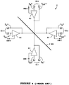
- FIGURE 4 depicts a generic multiplexer module, according to the present invention.
- Figure 3A depicts a single-bit ring bus 102 formed on an
integrated circuit chip 104 that may be an ASIC that includes circuitry formed on sub-sections. In the embodiment of Figure 3A, ring bus 102 includes M=4 two-way (e.g., X=2, or 2:1) multiplexer modules 106-0, 106-1, 106-2 and 106-3. Each multiplexer module defines an I/O node that may be coupled through the bus to one or more sub-sections or circuits onIC chip 104. In an IC with an N-bit wide bus, what is shown in Figure 3A would be replicated N times, with each ARB signal coupled to N multiplexer modules. - In the embodiment shown, each multiplexer module has two input ports, and output port, and an arbitration port. The multiplexer modules are two-way in that the multiplexer output port is coupled to a chosen one of the two input ports, the coupling being determined by the state of the signal coupled to the arbitration port.
- For example, multiplexer 106-0 has a first input port coupled to receive an I/O signal Din0 that is provided as an output (Dout1) by multiplexer 106-1. Multiplexer 106-0 has a second input port coupled to receive an I/O signal LOCALout0 that may be coupled to one or more sub-sections or circuits on the
IC chip 104. Multiplexer 106-0 also has an arbitration port coupled to receive an arbitration signal ARB-0, and an output port that couples an output signal Dout0 to an input port on an adjacent multiplexer, here module 106-3. - As shown by the voltage waveforms in Figure 3B, in the preferred embodiment, when ARB-0 is a digital "1", Dout0 is Din0, and when ARB-0 is a digital "0", Dout0 is LOCALout0. Figure 4 depicts a generic implementation of multiplexer module 106-0, as comprising two NMOS field effect transistors N4, N5 and an inverter I4. Of course other implementations could be used, including implementations that invert the polarity of the arbitration signal result in Dout being Din0 when ARB-0 is a "0", and being LOCALout0 when ARB-0 is "1".
- While the embodiment shown in Figure 4 represents a unidirectional multiplexer unit, those skilled in the art will recognize that a bidirectional multiplexer unit could instead be provided. The use of bidirectional multiplexer units would permit a ring bus structure according to the present invention to operate bidirectionally. Thus, with respect to Figure 3A, a signal coupled to
D IN0 might be passed across the ring toLOCAL OUT0, or a signal coupled toLOCAL OUT0 might be passed across the ring toD IN0. - At this juncture, similarities and differences between a multiplexer module ring bus 102 configuration according to Figure 3A, and a tristate buffer module configuration according to Figure 1A will be pointed out.
- The configurations are similar in that a chosen I/O node associated with one module may be coupled to another node associated with another module, according to the state of the arbitration select signals. In Figure 3A, for example, if ARB-0 is "1", and ARB-1, ARB-2, and ARB-3 are "0", a Din0 signal will pass through MUX 106-1, MUX 106-2 and MUX 106-3, and will appear at the LOCALout0 node of MUX 106-0. As shown in Figure 3A, the same Din0 signal will also be present at the nodes Din1, Din2 and Din3. As such, bus 102 is a ring, as indicated in Figure 3A.
- In contrast to the prior art, however, the ring bus configuration of Figure 3A is point-to-point in that the output of one module is coupled only to one other module. For example, the output from module 106-0 sees the Din3 input of module 106-3, and nothing more. The internal circuitry associated with each multiplexer module isolates the module inputs from the load impedance coupled to the module output.
- As such, the output transistors within each multiplexer module see a smaller ZL load than is seen by the output transistors in a tristate buffer module in the prior art. Whereas the output impedance seen by the prior art tristate buffer configuration of Figure 1 was about sixteen equivalent loads, the output impedance seen by a multiplexer module according to the present invention is only about four equivalent loads. Typical signal transition time for a 2:1 multiplexer module will be about 500 ps, e.g., about twice as fast as a prior art tristate buffer.
- Because the multiplexer modules are less heavily loaded, they can operate with a rapid voltage slewrate using decreased output current (since CLΔV/Δt is decreased). As a result, the metal trace that forms the bus path between multiplexer modules may be of narrower width for a given resistivity relative to the width of a metal bus trace used in prior art Figure 1. For example, a typical metal trace width used to implement Figure 3A may be only 0.8 µm. The ability to use narrower metal traces advantageously provides greater flexibility when designing the IC chip layout, and can reduce the capacitive load associated with a wider metal trace.
- Even if the sum of the operating current required by the four multiplexer modules shown in Figure 3A should equal or even exceed the operating current required by a single enabled single prior art tristate buffer module, the present invention is still advantageous. In the present invention, the drive current is distributed among the various multiplexer modules, whereas in the prior art, all of the drive current is provided by the one enabled tristate buffer. As a result, it is easier to fabricate lower current multiplexer modules than large current handling tristate buffer modules.
- Contention per se is not a problem with the present invention. In Figure 3A, even if more than one ARB arbitration signal is somehow simultaneously on (e.g., "1"), neither the selected multiplexer modules nor
IC 104 is damaged. - This is in contrast to what can result with the prior art configuration of Figure 1, wherein two (or more) high output current tristate buffer modules may attempt to drive each other.
- In the present invention, if quasi-contention results in the simultaneous selection of two or more multiplexer modules, the proper "0" or "1" state of the bit coupled to bus 102 may be erroneous, but thermal damage to the buffer modules or the IC would not occur. In a multi-bit bus configuration, quasi-contention might corrupt one or more bits (e.g., a "0" might become a "1" or vice versa) but damage to the IC would not necessarily occur.
- Because contention or quasi-contention does not present a problem that can damage or destroy
IC 104, the present invention may readily be tested using conventional test protocols and test equipment. For example, scanning test protocols may be used to rapidly testIC 104, in contrast to techniques that must be used to attempt to testprior art IC 4. - Although the preferred embodiment shown in Figure 3A depicts four 2:1 multiplexer modules, as few as two 2:1 multiplexer modules may be used to implement a bus. Ring topology buses used in networks may, for example, use as many as twenty or more 2:1 multiplexer modules. Further, X:1 switching modules may be implemented other than as conventional multiplexer units.
- As noted, the use of 2:1 (e.g., X=2) multiplexers per node results in the formation of a single data ring. However, for larger buses with many loads, it may be advantageous to use 3:1 (or arbitrarily X:1) multiplexers. Increasing X from 2 to 3 will increase the load per multiplier, as each multiplexer will then have to drive the node nearest it in two dimensions. However, increasing X will decrease the total number of elements in any one bus ring.
- An example of such an arrangement would be a bus with 16 nodes, effectively the configuration of Figure 3A, repeated four times, with vertically oriented ring buses passing through each node. While each node would then drive two loads (e.g., the adjacent load in the same plane, and the adjacent load "above"), the farthest distance between two loads decreases. The decrease is from 15 nodes for a single ring bus, to 6 nodes, namely three nodes in the horizontal plane and three nodes in the vertical plane.
- Thus, in general, an X:1 multiplexer module configuration will define an X-dimensional cube. For the 2:1 multiplexer module configuration of Figure 3A, X=2 and a two-dimensional planar configuration is defined. Where X=2, the output of each multiplexer module is coupled to [X-1] or one input on an adjacent module. If X=3 (e.g., if 3:1 multiplexer modules are used), a three-dimensional cube configuration would be realized. In a three-way configuration, each multiplexer output (Dout) would fanout to [X-1] or 2 inputs on other of the modules.
- To recapitulate, the use of multiplexer modules enables the present invention to be easily implemented with relatively low current-handling multiplexer transistors. The IC chip area required to implement the present invention does not exceed the chip area required to implement a conventional tristate buffer configuration having the same number of input/output nodes. Because each multiplexer module sources or sinks relatively little current, the metal trace used to implement the ring bus shown in Figure 3A may be thinner than would be the case for the bus shown in prior art Figure 1. Because contention damage is not present, the present invention lends itself to rapid testing using standard test techniques and equipment, including scanning.
- Modifications and variations may be made to the disclosed embodiments without departing from the subject and spirit of the invention as defined by the following claims.
Claims (10)
- A system, fabricated on an integrated circuit, for coupling data between M nodes, where M is an integer ≧ 2, the system comprising:
M modules each module having a first input coupled to a Din input node, having a second input coupled to a local output node, having an arbitration node coupled to an arbitration signal, and having an output node Dout that is coupled to said first input node of said same module when said first arbitration signal is in a first state and is coupled to said second input node of said same module when said first arbitration signal is in a second state; and
a conductive bus providing electrical coupling between adjacent said modules such that the Din input node of an Mi module is coupled to the Dout output node of an Mi+1th module, and the Din input node of the Mth module is coupled to the Dout output node of the Mi=0th module, where i is an integer 0≦i≦M-1;
wherein signal states of the arbitration signal coupled to each module define a signal path on said conductive bus between a desired input node on one module and an output node on another module, the modules so coupled providing point-to-point coupling. - The system of claim 1, wherein each said module is a 2:1 multiplexer unit.
- The system of claim 1 or 2, wherein for each said module, the module output node is buffered from said module's input nodes.
- The system of claim 1, wherein M =2, and the system includes:
a first module comprising a first 2:1 multiplexer unit having a first input coupled to a first input node, having a second input coupled to a first local output node, having an arbitration node coupled to a first arbitration signal, and having an output node that is coupled to said first input node of said first multiplexer unit when said first arbitration signal is in a first state and is coupled to said second input node of said first multiplexer unit when said first arbitration signal is in a second state;
a second module comprising a second 2:1 multiplexer unit having a first input coupled to a second input node and coupleable via a first portion of a conductive bus to said output node of said first multiplexer unit, having a second input coupled to a second local output node, having an arbitration node coupled to a second arbitration signal, and having an output node that is coupled to said first input node of said second multiplexer unit when said second arbitration signal is in a first state and is coupled to said second input node of said second multiplexer unit when said second arbitration signal is in a second state, said output node also coupled via a second portion of said conductive bus to said first input node of said first multiplexer unit; and
said conductive bus includes at least said first portion and said second portion;
wherein signal states of said first arbitration signal and said second arbitration signal define a signal path on said conductive bus between a desired input node on one multiplexer unit and the output node on the remaining multiplexer unit. - The system of claim 1, wherein each said module is fabricated with metal-oxide-semiconductor transistors.
- A method for coupling data between M nodes on an integrated circuit, where M is an integer ≧ 2, the method comprising the following steps:(a) providing M modules each module having a first input coupled to a Din input node, having a second input coupled to a local output node, having an arbitration node coupled to an arbitration signal, and having an output node Dout that is coupled to said first input node of said same module when said first arbitration signal is in a first state and is coupled to said second input node of said same module when said first arbitration signal is in a second state; and(b) providing a conductive bus providing electrical coupling between adjacent said modules such that the Din input node of an Mi module is coupled to the Dout output node of an Mi+1th module, and the Din input node of the Mth module is coupled to the Dout output node of the Mi=0th module, where i is an integer 0≦i≦M-1;wherein signal states of the arbitration signal coupled to each module define a signal path on said conductive bus between a desired input node on one module and an output node on another module, the modules so coupled providing point-to-point coupling.
- The method of claim 6, wherein at step (a) each said module is a 2:1 multiplexer unit.
- The method of claim 6 or 7, wherein step (a) includes providing modules having an output node that is buffered from each module's input nodes.
- The method of claim 6, wherein M =2, and step (a) includes:
providing a first module comprising a first 2:1 multiplexer unit having a first input coupled to a first input node, having a second input coupled to a first local output node, having an arbitration node coupled to a first arbitration signal, and having an output node that is coupled to said first input node of said first multiplexer unit when said first arbitration signal is in a first state and is coupled to said second input node of said second multiplexer unit when said first arbitration signal is in a second state; and
providing a second module comprising a second 2:1 multiplexer unit having a first input coupled to a second input node and coupleable via a first portion of a conductive bus to said output node of said first multiplexer unit, having a second input coupled to a second local output node, having an arbitration node coupled to a second arbitration signal, and having an output node that is coupled to said first input node of said second multiplexer unit when said second arbitration signal is in a first state and is coupled to said second input node of said second multiplexer unit when said second arbitration signal is in a second state, said output node also coupled via a second portion of said conductive bus to said first input node of said first multiplexer unit;
said conductive bus including at least said first portion and said second portion;
wherein signal states of said first arbitration signal and said second arbitration signal define a signal path on said conductive bus between a desired input node on one multiplexer unit and the output node on the remaining multiplexer unit. - The method of claim 6, wherein at step (a), each said module is fabricated with metal-oxide-semiconductor transistors.
Applications Claiming Priority (2)
| Application Number | Priority Date | Filing Date | Title |
|---|---|---|---|
| US390052 | 1995-02-17 | ||
| US08/390,052 US5555540A (en) | 1995-02-17 | 1995-02-17 | ASIC bus structure |
Publications (3)
| Publication Number | Publication Date |
|---|---|
| EP0727747A2 true EP0727747A2 (en) | 1996-08-21 |
| EP0727747A3 EP0727747A3 (en) | 2001-04-04 |
| EP0727747B1 EP0727747B1 (en) | 2004-01-21 |
Family
ID=23540837
Family Applications (1)
| Application Number | Title | Priority Date | Filing Date |
|---|---|---|---|
| EP96102074A Expired - Lifetime EP0727747B1 (en) | 1995-02-17 | 1996-02-13 | ASIC bus structure based on multiplexer |
Country Status (4)
| Country | Link |
|---|---|
| US (2) | US5555540A (en) |
| EP (1) | EP0727747B1 (en) |
| JP (1) | JP3022763B2 (en) |
| DE (1) | DE69631351T2 (en) |
Cited By (4)
| Publication number | Priority date | Publication date | Assignee | Title |
|---|---|---|---|---|
| EP0929042A2 (en) * | 1998-01-12 | 1999-07-14 | Nec Corporation | Bus controller in a data processor |
| US6600790B1 (en) | 1996-10-30 | 2003-07-29 | Hitachi, Ltd. | Gap-coupling bus system |
| GB2399434A (en) * | 2003-03-28 | 2004-09-15 | Hewlett Packard Development Co | Integrated circuit with debug bus |
| GB2399908A (en) * | 2003-03-28 | 2004-09-29 | Hewlett Packard Development Co | A bus interface module for a debug bus |
Families Citing this family (73)
| Publication number | Priority date | Publication date | Assignee | Title |
|---|---|---|---|---|
| US6028837A (en) * | 1996-08-27 | 2000-02-22 | National Semiconductor Corporation | Ether ring architecture for local area networks |
| US6317804B1 (en) * | 1998-11-30 | 2001-11-13 | Philips Semiconductors Inc. | Concurrent serial interconnect for integrating functional blocks in an integrated circuit device |
| US6647450B1 (en) | 1999-10-06 | 2003-11-11 | Cradle Technologies, Inc. | Multiprocessor computer systems with command FIFO buffer at each target device |
| US6807165B2 (en) | 2000-11-08 | 2004-10-19 | Meshnetworks, Inc. | Time division protocol for an ad-hoc, peer-to-peer radio network having coordinating channel access to shared parallel data channels with separate reservation channel |
| US7072650B2 (en) * | 2000-11-13 | 2006-07-04 | Meshnetworks, Inc. | Ad hoc peer-to-peer mobile radio access system interfaced to the PSTN and cellular networks |
| US6873839B2 (en) | 2000-11-13 | 2005-03-29 | Meshnetworks, Inc. | Prioritized-routing for an ad-hoc, peer-to-peer, mobile radio access system |
| US7151769B2 (en) * | 2001-03-22 | 2006-12-19 | Meshnetworks, Inc. | Prioritized-routing for an ad-hoc, peer-to-peer, mobile radio access system based on battery-power levels and type of service |
| JP2004531971A (en) * | 2001-06-14 | 2004-10-14 | メッシュネットワークス インコーポレーティッド | A routing protocol embedded under the internet protocol routing layer of the software architecture protocol stack in mobile ad hoc networks |
| US7206294B2 (en) | 2001-08-15 | 2007-04-17 | Meshnetworks, Inc. | Movable access points and repeaters for minimizing coverage and capacity constraints in a wireless communications network and a method for using the same |
| US7072323B2 (en) * | 2001-08-15 | 2006-07-04 | Meshnetworks, Inc. | System and method for performing soft handoff in a wireless data network |
| US7349380B2 (en) * | 2001-08-15 | 2008-03-25 | Meshnetworks, Inc. | System and method for providing an addressing and proxy scheme for facilitating mobility of wireless nodes between wired access points on a core network of a communications network |
| US7613458B2 (en) * | 2001-08-28 | 2009-11-03 | Meshnetworks, Inc. | System and method for enabling a radio node to selectably function as a router in a wireless communications network |
| US7145903B2 (en) * | 2001-09-06 | 2006-12-05 | Meshnetworks, Inc. | Multi-master bus architecture for system-on-chip designs |
| JP4139775B2 (en) * | 2001-09-25 | 2008-08-27 | メシュネットワークス、インコーポレイテッド | Systems and methods employing algorithms and protocols for operating Carrier Sense Multiple Access (CSMA) protocols in wireless networks |
| US6754188B1 (en) | 2001-09-28 | 2004-06-22 | Meshnetworks, Inc. | System and method for enabling a node in an ad-hoc packet-switched wireless communications network to route packets based on packet content |
| US6768730B1 (en) | 2001-10-11 | 2004-07-27 | Meshnetworks, Inc. | System and method for efficiently performing two-way ranging to determine the location of a wireless node in a communications network |
| US6937602B2 (en) * | 2001-10-23 | 2005-08-30 | Meshnetworks, Inc. | System and method for providing a congestion optimized address resolution protocol for wireless ad-hoc networks |
| US6771666B2 (en) | 2002-03-15 | 2004-08-03 | Meshnetworks, Inc. | System and method for trans-medium address resolution on an ad-hoc network with at least one highly disconnected medium having multiple access points to other media |
| US6982982B1 (en) | 2001-10-23 | 2006-01-03 | Meshnetworks, Inc. | System and method for providing a congestion optimized address resolution protocol for wireless ad-hoc networks |
| US7181214B1 (en) | 2001-11-13 | 2007-02-20 | Meshnetworks, Inc. | System and method for determining the measure of mobility of a subscriber device in an ad-hoc wireless network with fixed wireless routers and wide area network (WAN) access points |
| US7136587B1 (en) | 2001-11-15 | 2006-11-14 | Meshnetworks, Inc. | System and method for providing simulated hardware-in-the-loop testing of wireless communications networks |
| US6728545B1 (en) | 2001-11-16 | 2004-04-27 | Meshnetworks, Inc. | System and method for computing the location of a mobile terminal in a wireless communications network |
| US7221686B1 (en) | 2001-11-30 | 2007-05-22 | Meshnetworks, Inc. | System and method for computing the signal propagation time and the clock correction for mobile stations in a wireless network |
| US7190672B1 (en) | 2001-12-19 | 2007-03-13 | Meshnetworks, Inc. | System and method for using destination-directed spreading codes in a multi-channel metropolitan area wireless communications network |
| US7180875B1 (en) | 2001-12-20 | 2007-02-20 | Meshnetworks, Inc. | System and method for performing macro-diversity selection and distribution of routes for routing data packets in Ad-Hoc networks |
| US7280545B1 (en) | 2001-12-20 | 2007-10-09 | Nagle Darragh J | Complex adaptive routing system and method for a nodal communication network |
| US7106707B1 (en) | 2001-12-20 | 2006-09-12 | Meshnetworks, Inc. | System and method for performing code and frequency channel selection for combined CDMA/FDMA spread spectrum communication systems |
| US7072618B1 (en) | 2001-12-21 | 2006-07-04 | Meshnetworks, Inc. | Adaptive threshold selection system and method for detection of a signal in the presence of interference |
| KR100477641B1 (en) * | 2002-01-15 | 2005-03-23 | 삼성전자주식회사 | Bus system and path decision method therefor |
| US6674790B1 (en) | 2002-01-24 | 2004-01-06 | Meshnetworks, Inc. | System and method employing concatenated spreading sequences to provide data modulated spread signals having increased data rates with extended multi-path delay spread |
| US6617990B1 (en) | 2002-03-06 | 2003-09-09 | Meshnetworks | Digital-to-analog converter using pseudo-random sequences and a method for using the same |
| US7058018B1 (en) | 2002-03-06 | 2006-06-06 | Meshnetworks, Inc. | System and method for using per-packet receive signal strength indication and transmit power levels to compute path loss for a link for use in layer II routing in a wireless communication network |
| DE60321895D1 (en) | 2002-03-15 | 2008-08-14 | Meshnetworks Inc | SYSTEM AND METHOD FOR SELF-CONFIGURATION AND DISCOVERY OF IP-TO-MAC ADDRESS PICTURES AND THE GATEWAY PRESENCE |
| US6904021B2 (en) | 2002-03-15 | 2005-06-07 | Meshnetworks, Inc. | System and method for providing adaptive control of transmit power and data rate in an ad-hoc communication network |
| US6987795B1 (en) | 2002-04-08 | 2006-01-17 | Meshnetworks, Inc. | System and method for selecting spreading codes based on multipath delay profile estimation for wireless transceivers in a communication network |
| US7200149B1 (en) | 2002-04-12 | 2007-04-03 | Meshnetworks, Inc. | System and method for identifying potential hidden node problems in multi-hop wireless ad-hoc networks for the purpose of avoiding such potentially problem nodes in route selection |
| US6580981B1 (en) | 2002-04-16 | 2003-06-17 | Meshnetworks, Inc. | System and method for providing wireless telematics store and forward messaging for peer-to-peer and peer-to-peer-to-infrastructure a communication network |
| US7107498B1 (en) | 2002-04-16 | 2006-09-12 | Methnetworks, Inc. | System and method for identifying and maintaining reliable infrastructure links using bit error rate data in an ad-hoc communication network |
| US7113488B2 (en) * | 2002-04-24 | 2006-09-26 | International Business Machines Corporation | Reconfigurable circular bus |
| US7142524B2 (en) * | 2002-05-01 | 2006-11-28 | Meshnetworks, Inc. | System and method for using an ad-hoc routing algorithm based on activity detection in an ad-hoc network |
| US6970444B2 (en) | 2002-05-13 | 2005-11-29 | Meshnetworks, Inc. | System and method for self propagating information in ad-hoc peer-to-peer networks |
| US7016306B2 (en) * | 2002-05-16 | 2006-03-21 | Meshnetworks, Inc. | System and method for performing multiple network routing and provisioning in overlapping wireless deployments |
| US7284268B2 (en) | 2002-05-16 | 2007-10-16 | Meshnetworks, Inc. | System and method for a routing device to securely share network data with a host utilizing a hardware firewall |
| US7167715B2 (en) * | 2002-05-17 | 2007-01-23 | Meshnetworks, Inc. | System and method for determining relative positioning in AD-HOC networks |
| US7106703B1 (en) | 2002-05-28 | 2006-09-12 | Meshnetworks, Inc. | System and method for controlling pipeline delays by adjusting the power levels at which nodes in an ad-hoc network transmit data packets |
| US7054126B2 (en) * | 2002-06-05 | 2006-05-30 | Meshnetworks, Inc. | System and method for improving the accuracy of time of arrival measurements in a wireless ad-hoc communications network |
| US6744766B2 (en) | 2002-06-05 | 2004-06-01 | Meshnetworks, Inc. | Hybrid ARQ for a wireless Ad-Hoc network and a method for using the same |
| US6687259B2 (en) | 2002-06-05 | 2004-02-03 | Meshnetworks, Inc. | ARQ MAC for ad-hoc communication networks and a method for using the same |
| US7610027B2 (en) * | 2002-06-05 | 2009-10-27 | Meshnetworks, Inc. | Method and apparatus to maintain specification absorption rate at a wireless node |
| AU2003238968A1 (en) * | 2002-06-11 | 2003-12-22 | Meshnetworks, Inc. | System and method for multicast media access in ad-hoc communication networks |
| US7215638B1 (en) | 2002-06-19 | 2007-05-08 | Meshnetworks, Inc. | System and method to provide 911 access in voice over internet protocol systems without compromising network security |
| US7072432B2 (en) * | 2002-07-05 | 2006-07-04 | Meshnetworks, Inc. | System and method for correcting the clock drift and maintaining the synchronization of low quality clocks in wireless networks |
| US7796570B1 (en) | 2002-07-12 | 2010-09-14 | Meshnetworks, Inc. | Method for sparse table accounting and dissemination from a mobile subscriber device in a wireless mobile ad-hoc network |
| US7046962B1 (en) | 2002-07-18 | 2006-05-16 | Meshnetworks, Inc. | System and method for improving the quality of range measurement based upon historical data |
| US7042867B2 (en) * | 2002-07-29 | 2006-05-09 | Meshnetworks, Inc. | System and method for determining physical location of a node in a wireless network during an authentication check of the node |
| US7373561B2 (en) * | 2002-10-29 | 2008-05-13 | Broadcom Corporation | Integrated packet bit error rate tester for 10G SERDES |
| US7522537B2 (en) * | 2003-01-13 | 2009-04-21 | Meshnetworks, Inc. | System and method for providing connectivity between an intelligent access point and nodes in a wireless network |
| WO2004084022A2 (en) | 2003-03-13 | 2004-09-30 | Meshnetworks, Inc. | Real-time system and method for computing location of mobile subcriber in a wireless ad-hoc network |
| US7171220B2 (en) * | 2003-03-14 | 2007-01-30 | Meshnetworks, Inc. | System and method for analyzing the precision of geo-location services in a wireless network terminal |
| WO2004114690A1 (en) * | 2003-06-05 | 2004-12-29 | Meshnetworks, Inc. | Optimal routing in ad hac wireless communication network |
| US7734809B2 (en) * | 2003-06-05 | 2010-06-08 | Meshnetworks, Inc. | System and method to maximize channel utilization in a multi-channel wireless communication network |
| WO2004110082A1 (en) * | 2003-06-05 | 2004-12-16 | Meshnetworks, Inc. | System and method for determining location of a device in a wireless communication network |
| EP1652207A4 (en) * | 2003-06-05 | 2011-12-28 | Meshnetworks Inc | System and method for determining synchronization point in ofdm modems for accurate time of flight measurement |
| EP1632044B1 (en) * | 2003-06-06 | 2011-10-19 | Meshnetworks, Inc. | Method to improve the overall performance of a wireless communication network |
| WO2004109473A2 (en) | 2003-06-06 | 2004-12-16 | Meshnetworks, Inc. | System and method to provide fairness and service differentiation in ad-hoc networks |
| WO2004109474A2 (en) * | 2003-06-06 | 2004-12-16 | Meshnetworks, Inc. | System and method for characterizing the quality of a link in a wireless network |
| EP1632093A2 (en) | 2003-06-06 | 2006-03-08 | Meshnetworks, Inc. | System and method for identifying the floor number where a firefighter in need of help is located using received signal strength indicator and signal propagation time |
| US7167463B2 (en) * | 2004-10-07 | 2007-01-23 | Meshnetworks, Inc. | System and method for creating a spectrum agile wireless multi-hopping network |
| CN100447769C (en) * | 2005-06-06 | 2008-12-31 | 上海奇码数字信息有限公司 | Bus system |
| US8699514B2 (en) * | 2007-01-12 | 2014-04-15 | Broadcom Corporation | Multi-rate MAC to PHY interface |
| US8122279B2 (en) * | 2008-04-21 | 2012-02-21 | Kabushiki Kaisha Toshiba | Multiphase clocking systems with ring bus architecture |
| US8429391B2 (en) | 2010-04-16 | 2013-04-23 | Micron Technology, Inc. | Boot partitions in memory devices and systems |
| US8451664B2 (en) | 2010-05-12 | 2013-05-28 | Micron Technology, Inc. | Determining and using soft data in memory devices and systems |
Citations (2)
| Publication number | Priority date | Publication date | Assignee | Title |
|---|---|---|---|---|
| US4383314A (en) * | 1981-01-12 | 1983-05-10 | Burroughs Corporation | Circular access linkage loop configuration for system communication |
| US5329529A (en) * | 1993-04-02 | 1994-07-12 | Thomson Consumer Electronics, Inc. | Digital data arbitration apparatus |
Family Cites Families (5)
| Publication number | Priority date | Publication date | Assignee | Title |
|---|---|---|---|---|
| US3838296A (en) * | 1973-10-29 | 1974-09-24 | Nat Semiconductor Corp | Emitter coupled logic transistor circuit |
| US4858232A (en) * | 1988-05-20 | 1989-08-15 | Dsc Communications Corporation | Distributed switching system |
| GB9007600D0 (en) * | 1990-04-04 | 1990-05-30 | Hunting Communication Tech | Ring communication system |
| US5111455A (en) * | 1990-08-24 | 1992-05-05 | Avantek, Inc. | Interleaved time-division multiplexor with phase-compensated frequency doublers |
| US5680594A (en) * | 1995-05-24 | 1997-10-21 | Eastman Kodak Company | Asic bus interface having a master state machine and a plurality of synchronizing state machines for controlling subsystems operating at different clock frequencies |
-
1995
- 1995-02-17 US US08/390,052 patent/US5555540A/en not_active Expired - Fee Related
-
1996
- 1996-02-13 DE DE69631351T patent/DE69631351T2/en not_active Expired - Fee Related
- 1996-02-13 EP EP96102074A patent/EP0727747B1/en not_active Expired - Lifetime
- 1996-02-15 JP JP8052329A patent/JP3022763B2/en not_active Expired - Fee Related
- 1996-06-24 US US08/669,631 patent/US5751699A/en not_active Expired - Lifetime
Patent Citations (2)
| Publication number | Priority date | Publication date | Assignee | Title |
|---|---|---|---|---|
| US4383314A (en) * | 1981-01-12 | 1983-05-10 | Burroughs Corporation | Circular access linkage loop configuration for system communication |
| US5329529A (en) * | 1993-04-02 | 1994-07-12 | Thomson Consumer Electronics, Inc. | Digital data arbitration apparatus |
Cited By (9)
| Publication number | Priority date | Publication date | Assignee | Title |
|---|---|---|---|---|
| US6600790B1 (en) | 1996-10-30 | 2003-07-29 | Hitachi, Ltd. | Gap-coupling bus system |
| EP0929042A2 (en) * | 1998-01-12 | 1999-07-14 | Nec Corporation | Bus controller in a data processor |
| EP0929042A3 (en) * | 1998-01-12 | 2002-06-19 | Nec Corporation | Bus controller in a data processor |
| GB2399434A (en) * | 2003-03-28 | 2004-09-15 | Hewlett Packard Development Co | Integrated circuit with debug bus |
| GB2399908A (en) * | 2003-03-28 | 2004-09-29 | Hewlett Packard Development Co | A bus interface module for a debug bus |
| GB2399434B (en) * | 2003-03-28 | 2006-03-22 | Hewlett Packard Development Co | An integrated circuit having a debug bus |
| GB2399908B (en) * | 2003-03-28 | 2006-04-05 | Hewlett Packard Development Co | A bus interface module |
| US7146538B2 (en) | 2003-03-28 | 2006-12-05 | Hewlett-Packard Development Company, L.P. | Bus interface module |
| US7188277B2 (en) | 2003-03-28 | 2007-03-06 | Hewlett-Packard Development Company, L.P. | Integrated circuit |
Also Published As
| Publication number | Publication date |
|---|---|
| JPH08335128A (en) | 1996-12-17 |
| JP3022763B2 (en) | 2000-03-21 |
| DE69631351D1 (en) | 2004-02-26 |
| US5555540A (en) | 1996-09-10 |
| US5751699A (en) | 1998-05-12 |
| DE69631351T2 (en) | 2004-11-04 |
| EP0727747B1 (en) | 2004-01-21 |
| EP0727747A3 (en) | 2001-04-04 |
Similar Documents
| Publication | Publication Date | Title |
|---|---|---|
| EP0727747B1 (en) | ASIC bus structure based on multiplexer | |
| US5311081A (en) | Data bus using open drain drivers and differential receivers together with distributed termination impedances | |
| US7868790B2 (en) | Single ended pseudo differential interconnection circuit and single ended pseudo differential signaling method | |
| US6421784B1 (en) | Programmable delay circuit having a fine delay element selectively receives input signal and output signal of coarse delay element | |
| US4500988A (en) | VLSI Wired-OR driver/receiver circuit | |
| US5086427A (en) | Clocked logic circuitry preventing double driving on shared data bus | |
| US6552410B1 (en) | Programmable antifuse interfacing a programmable logic and a dedicated device | |
| AU644141B2 (en) | A method of controlling a router circuit | |
| US6760857B1 (en) | System having both externally and internally generated clock signals being asserted on the same clock pin in normal and test modes of operation respectively | |
| US7043670B2 (en) | Reducing the effect of simultaneous switching noise | |
| US6657460B2 (en) | Spatially filtered data bus drivers and receivers and method of operating same | |
| US6071003A (en) | Method and apparatus for locating critical speed paths in integrated circuits using a clock driver circuit with variable delay | |
| US20070240094A1 (en) | Partially gated mux-latch keeper | |
| US5818263A (en) | Method and apparatus for locating and improving race conditions in VLSI integrated circuits | |
| JP2725601B2 (en) | I / O buffer | |
| US6242941B1 (en) | Reducing I/O noise when leaving programming mode | |
| US6990076B1 (en) | Synchronous bi-directional data transfer having increased bandwidth and scan test features | |
| US11313904B2 (en) | Testing device and testing method | |
| US5638008A (en) | Method and apparatus for generating an asynchronously clocked signal in a synchronously clocked programmable device | |
| US5363494A (en) | Bus interface circuit for connecting bus lines having different bit ranges | |
| US6678846B1 (en) | Semiconductor integrated circuit with a scan path circuit | |
| EP1324208A1 (en) | Circuit device for transmitting bus signals | |
| US20020172232A1 (en) | Combination multiplexer and tristate driver circuit | |
| US6452417B1 (en) | I/O cell architecture for CPLDs | |
| US5399923A (en) | Field programmable gate array device with antifuse overcurrent protection |
Legal Events
| Date | Code | Title | Description |
|---|---|---|---|
| PUAI | Public reference made under article 153(3) epc to a published international application that has entered the european phase |
Free format text: ORIGINAL CODE: 0009012 |
|
| AK | Designated contracting states |
Kind code of ref document: A2 Designated state(s): DE FR GB NL SE |
|
| PUAL | Search report despatched |
Free format text: ORIGINAL CODE: 0009013 |
|
| AK | Designated contracting states |
Kind code of ref document: A3 Designated state(s): DE FR GB NL SE |
|
| RIC1 | Information provided on ipc code assigned before grant |
Free format text: 7G 06F 13/14 A, 7G 06F 13/40 B |
|
| 17P | Request for examination filed |
Effective date: 20011001 |
|
| 17Q | First examination report despatched |
Effective date: 20020503 |
|
| GRAP | Despatch of communication of intention to grant a patent |
Free format text: ORIGINAL CODE: EPIDOSNIGR1 |
|
| RTI1 | Title (correction) |
Free format text: ASIC BUS STRUCTURE BASED ON MULTIPLEXER |
|
| GRAS | Grant fee paid |
Free format text: ORIGINAL CODE: EPIDOSNIGR3 |
|
| GRAA | (expected) grant |
Free format text: ORIGINAL CODE: 0009210 |
|
| AK | Designated contracting states |
Kind code of ref document: B1 Designated state(s): DE FR GB NL SE |
|
| PG25 | Lapsed in a contracting state [announced via postgrant information from national office to epo] |
Ref country code: NL Free format text: LAPSE BECAUSE OF FAILURE TO SUBMIT A TRANSLATION OF THE DESCRIPTION OR TO PAY THE FEE WITHIN THE PRESCRIBED TIME-LIMIT Effective date: 20040121 |
|
| REG | Reference to a national code |
Ref country code: GB Ref legal event code: FG4D |
|
| PGFP | Annual fee paid to national office [announced via postgrant information from national office to epo] |
Ref country code: SE Payment date: 20040204 Year of fee payment: 9 |
|
| PGFP | Annual fee paid to national office [announced via postgrant information from national office to epo] |
Ref country code: NL Payment date: 20040205 Year of fee payment: 9 |
|
| PGFP | Annual fee paid to national office [announced via postgrant information from national office to epo] |
Ref country code: FR Payment date: 20040210 Year of fee payment: 9 |
|
| PGFP | Annual fee paid to national office [announced via postgrant information from national office to epo] |
Ref country code: DE Payment date: 20040226 Year of fee payment: 9 |
|
| REF | Corresponds to: |
Ref document number: 69631351 Country of ref document: DE Date of ref document: 20040226 Kind code of ref document: P |
|
| PG25 | Lapsed in a contracting state [announced via postgrant information from national office to epo] |
Ref country code: SE Free format text: LAPSE BECAUSE OF FAILURE TO SUBMIT A TRANSLATION OF THE DESCRIPTION OR TO PAY THE FEE WITHIN THE PRESCRIBED TIME-LIMIT Effective date: 20040421 |
|
| NLV1 | Nl: lapsed or annulled due to failure to fulfill the requirements of art. 29p and 29m of the patents act | ||
| ET | Fr: translation filed | ||
| PLBE | No opposition filed within time limit |
Free format text: ORIGINAL CODE: 0009261 |
|
| STAA | Information on the status of an ep patent application or granted ep patent |
Free format text: STATUS: NO OPPOSITION FILED WITHIN TIME LIMIT |
|
| 26N | No opposition filed |
Effective date: 20041022 |
|
| PG25 | Lapsed in a contracting state [announced via postgrant information from national office to epo] |
Ref country code: DE Free format text: LAPSE BECAUSE OF NON-PAYMENT OF DUE FEES Effective date: 20050901 |
|
| PG25 | Lapsed in a contracting state [announced via postgrant information from national office to epo] |
Ref country code: FR Free format text: LAPSE BECAUSE OF NON-PAYMENT OF DUE FEES Effective date: 20051031 |
|
| REG | Reference to a national code |
Ref country code: FR Ref legal event code: ST Effective date: 20051031 |
|
| PGFP | Annual fee paid to national office [announced via postgrant information from national office to epo] |
Ref country code: GB Payment date: 20070207 Year of fee payment: 12 |
|
| GBPC | Gb: european patent ceased through non-payment of renewal fee |
Effective date: 20080213 |
|
| PG25 | Lapsed in a contracting state [announced via postgrant information from national office to epo] |
Ref country code: GB Free format text: LAPSE BECAUSE OF NON-PAYMENT OF DUE FEES Effective date: 20080213 |