EP0727645A1 - Magnetic signal detector - Google Patents
Magnetic signal detector Download PDFInfo
- Publication number
- EP0727645A1 EP0727645A1 EP95929216A EP95929216A EP0727645A1 EP 0727645 A1 EP0727645 A1 EP 0727645A1 EP 95929216 A EP95929216 A EP 95929216A EP 95929216 A EP95929216 A EP 95929216A EP 0727645 A1 EP0727645 A1 EP 0727645A1
- Authority
- EP
- European Patent Office
- Prior art keywords
- magnetic field
- resistive element
- approximately
- biasing
- magnetic signal
- Prior art date
- Legal status (The legal status is an assumption and is not a legal conclusion. Google has not performed a legal analysis and makes no representation as to the accuracy of the status listed.)
- Granted
Links
Images


Classifications
-
- G—PHYSICS
- G01—MEASURING; TESTING
- G01D—MEASURING NOT SPECIALLY ADAPTED FOR A SPECIFIC VARIABLE; ARRANGEMENTS FOR MEASURING TWO OR MORE VARIABLES NOT COVERED IN A SINGLE OTHER SUBCLASS; TARIFF METERING APPARATUS; MEASURING OR TESTING NOT OTHERWISE PROVIDED FOR
- G01D5/00—Mechanical means for transferring the output of a sensing member; Means for converting the output of a sensing member to another variable where the form or nature of the sensing member does not constrain the means for converting; Transducers not specially adapted for a specific variable
- G01D5/12—Mechanical means for transferring the output of a sensing member; Means for converting the output of a sensing member to another variable where the form or nature of the sensing member does not constrain the means for converting; Transducers not specially adapted for a specific variable using electric or magnetic means
- G01D5/244—Mechanical means for transferring the output of a sensing member; Means for converting the output of a sensing member to another variable where the form or nature of the sensing member does not constrain the means for converting; Transducers not specially adapted for a specific variable using electric or magnetic means influencing characteristics of pulses or pulse trains; generating pulses or pulse trains
- G01D5/245—Mechanical means for transferring the output of a sensing member; Means for converting the output of a sensing member to another variable where the form or nature of the sensing member does not constrain the means for converting; Transducers not specially adapted for a specific variable using electric or magnetic means influencing characteristics of pulses or pulse trains; generating pulses or pulse trains using a variable number of pulses in a train
-
- G—PHYSICS
- G01—MEASURING; TESTING
- G01D—MEASURING NOT SPECIALLY ADAPTED FOR A SPECIFIC VARIABLE; ARRANGEMENTS FOR MEASURING TWO OR MORE VARIABLES NOT COVERED IN A SINGLE OTHER SUBCLASS; TARIFF METERING APPARATUS; MEASURING OR TESTING NOT OTHERWISE PROVIDED FOR
- G01D5/00—Mechanical means for transferring the output of a sensing member; Means for converting the output of a sensing member to another variable where the form or nature of the sensing member does not constrain the means for converting; Transducers not specially adapted for a specific variable
- G01D5/12—Mechanical means for transferring the output of a sensing member; Means for converting the output of a sensing member to another variable where the form or nature of the sensing member does not constrain the means for converting; Transducers not specially adapted for a specific variable using electric or magnetic means
- G01D5/14—Mechanical means for transferring the output of a sensing member; Means for converting the output of a sensing member to another variable where the form or nature of the sensing member does not constrain the means for converting; Transducers not specially adapted for a specific variable using electric or magnetic means influencing the magnitude of a current or voltage
- G01D5/142—Mechanical means for transferring the output of a sensing member; Means for converting the output of a sensing member to another variable where the form or nature of the sensing member does not constrain the means for converting; Transducers not specially adapted for a specific variable using electric or magnetic means influencing the magnitude of a current or voltage using Hall-effect devices
- G01D5/145—Mechanical means for transferring the output of a sensing member; Means for converting the output of a sensing member to another variable where the form or nature of the sensing member does not constrain the means for converting; Transducers not specially adapted for a specific variable using electric or magnetic means influencing the magnitude of a current or voltage using Hall-effect devices influenced by the relative movement between the Hall device and magnetic fields
-
- G—PHYSICS
- G01—MEASURING; TESTING
- G01P—MEASURING LINEAR OR ANGULAR SPEED, ACCELERATION, DECELERATION, OR SHOCK; INDICATING PRESENCE, ABSENCE, OR DIRECTION, OF MOVEMENT
- G01P3/00—Measuring linear or angular speed; Measuring differences of linear or angular speeds
- G01P3/42—Devices characterised by the use of electric or magnetic means
- G01P3/44—Devices characterised by the use of electric or magnetic means for measuring angular speed
- G01P3/48—Devices characterised by the use of electric or magnetic means for measuring angular speed by measuring frequency of generated current or voltage
- G01P3/481—Devices characterised by the use of electric or magnetic means for measuring angular speed by measuring frequency of generated current or voltage of pulse signals
- G01P3/487—Devices characterised by the use of electric or magnetic means for measuring angular speed by measuring frequency of generated current or voltage of pulse signals delivered by rotating magnets
-
- G—PHYSICS
- G01—MEASURING; TESTING
- G01R—MEASURING ELECTRIC VARIABLES; MEASURING MAGNETIC VARIABLES
- G01R33/00—Arrangements or instruments for measuring magnetic variables
- G01R33/02—Measuring direction or magnitude of magnetic fields or magnetic flux
- G01R33/06—Measuring direction or magnitude of magnetic fields or magnetic flux using galvano-magnetic devices
- G01R33/09—Magnetoresistive devices
-
- G—PHYSICS
- G11—INFORMATION STORAGE
- G11B—INFORMATION STORAGE BASED ON RELATIVE MOVEMENT BETWEEN RECORD CARRIER AND TRANSDUCER
- G11B5/00—Recording by magnetisation or demagnetisation of a record carrier; Reproducing by magnetic means; Record carriers therefor
-
- G—PHYSICS
- G11—INFORMATION STORAGE
- G11B—INFORMATION STORAGE BASED ON RELATIVE MOVEMENT BETWEEN RECORD CARRIER AND TRANSDUCER
- G11B5/00—Recording by magnetisation or demagnetisation of a record carrier; Reproducing by magnetic means; Record carriers therefor
- G11B5/127—Structure or manufacture of heads, e.g. inductive
- G11B5/33—Structure or manufacture of flux-sensitive heads, i.e. for reproduction only; Combination of such heads with means for recording or erasing only
- G11B5/39—Structure or manufacture of flux-sensitive heads, i.e. for reproduction only; Combination of such heads with means for recording or erasing only using magneto-resistive devices or effects
- G11B5/3903—Structure or manufacture of flux-sensitive heads, i.e. for reproduction only; Combination of such heads with means for recording or erasing only using magneto-resistive devices or effects using magnetic thin film layers or their effects, the films being part of integrated structures
Definitions
- the present invention relates to a magnetic signal detection apparatus utilizing a ferromagnetic thin film magneto-resistive element.
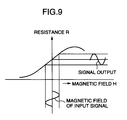
- a biasing magnet 3 by applying the biasing magnetic field Hb by a biasing magnet 3 in the direction of approximately 45° to the direction of the current I flowing through the thin film magneto-resistive element 2 as shown in a magneto-resistance characteristic of Fig. 9, an operating point at which high linearity and high reproduced output are attained is selected.
- numerals 4 and 5 denote power terminals for supplying the current to the thin film magneto-resistive element 2.
- Fig. 10 JP-B-1-45008
- numerals 6 and 8 denote power terminals
- numeral 7 denotes an output terminal
- numeral 9 denotes a biasing magnetic field
- numeral 10 denotes a signal magnetic field recording medium.
- the biasing magnetic field is applied in the direction of 45° to a longitudinal direction (current direction) of the resistive element.
- a longitudinal direction current direction
- the direction of magnetization M of the resistive element is oriented in the longitudinal direction of the resistive element by a shape effect.
- the magnetic signal detection apparatus of the present invention comprises an anisotropic resistive element arranged to face in a face-to-face fashion or perpendicularly to a magnetic signal recording surface on a substrate and made of a ferromagnetic metal thin film, and a magnetic filed application apparatus for applying a biasing magnetic field of a predetermined angle to said resistive element.
- the biasing magnetic field to the resistive element is no smaller than approximately ⁇ 47° and no larger than approximately ⁇ 75° to the direction of the current or the biasing magnetic field to the resistive element is no smaller than approximately ⁇ 105° and no larger than approximately ⁇ 133° to the direction of the current.
- the direction of application of Hb required to orient the magnetization M to a direction of substantially 45° to the longitudinal direction (the direction of current) of the resistive element is approximately 56° to the longitudinal direction of the resistive element.
- the biasing magnetic field strength to orient the magnetization to substantially 45° in the ferromagnetic thin film (MR film) is greater than approximately 10,000 Oe.
- Hb is relatively weak
- the magnetization is oriented in the direction of approximately 33°.
- the angle between the magnetization M and the current is made to approximately ⁇ 45° (or approximately ⁇ 135°) so that the reproduction characteristic of the magnetic signal is improved.
- a relation between the biasing magnetic field strength Hb and the biasing angle ⁇ is such that when Hb is increased, a difference ( ⁇ - ⁇ ) between the angle ⁇ of the biasing magnetic field strength Hb and the angle ⁇ of the magnetization M decreases.
- a neodium group having a large remanent magnetic flux density Br and a maximum magnetic flux density Brmax of approximately 13 KG is known.
- an applied magnetic flux strength on the resistive element is approximately 1400 Oe at maximum because the magnetic field is applied to the thin film resistive element through the thickness of the substrate (approximately 0.7 mm).
- the angle of the biasing magnetic field which results in approximately ⁇ 45° (or ⁇ 135°) between the magnetization M and the current is, from the formula (3), approximately ⁇ 47° (or ⁇ 133°).
- the applied magnetic field strength is preferably at least 140 Oe.
- the angle of the biasing magnetic field is approximately ⁇ 56° (or approximately ⁇ 124°).
- the angle of the biasing magnetic field is approximately ⁇ 47° ⁇ ⁇ 75° (or approximately ⁇ 105° ⁇ ⁇ 133°).
- the anisotropy energy Ku 5 ⁇ 40
- Hb of 140 Oe or 1400 Oe is applied to the MR film having the film thickness of 0.05 ⁇ m ⁇ 0.1 ⁇ m and the film width of 8 ⁇ m ⁇ 20 ⁇ m, the angle ⁇ for the maximum output is shown below.
- the anisotropy energy Ku 15 ⁇ 40, and when Hb of 140 Oe or 1400 Oe is applied to the MR film having the film thickness of 0.05 ⁇ m ⁇ 0.1 ⁇ m and the film width of 8 ⁇ m ⁇ 20 ⁇ m, the angle ⁇ for the maximum output is shown below.
- the biassing angle of the biasing magnet applied to the MR film is approximately ⁇ 47° ⁇ ⁇ 75°.
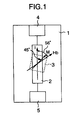
- Fig. 1 shows a construction of the thin film magneto-resistive element in one embodiment in which a biasing magnetic field is applied in the direction of 56° to the longitudinal direction (the direction of the current I) to a detection element which faces a magnetic signal recording medium.
- the biasing magnetic field Hb is applied by the biasing magnet 3 in the angle of 56° to the longitudinal direction (the direction of the current I) of the thin film magneto-resistive element 2 to orient the magnetization M to the angle of 45° to the longitudinal direction.
- Fig. 2 shows an arrangement of the detection element to the magnetic signal recording medium in other embodiment of the present invention.
- the thin film magneto-resistive elements are arranged at an interval of ⁇ /2 where ⁇ is a magnetic lattice pitch and the biasing magnetic field Hb is applied in the direction of approximately 56° so that the direction of magnetization is approximately 45° to the longitudinal direction of the resistive element.
- Fig. 3 shows an arrangement of the detection elements to the magnetic signal recording medium in a further embodiment of the present invention.
- the resistive elements are arranged at an interval of ⁇ and they are divided into first group and second group with a separation of 3 ⁇ /2 between the first resistive element group and the second resistive element group, and the biasing magnetic field Hb is applied in the direction of approximately 56° so that the magnetization is oriented to approximately 45° to the longitudinal direction of the resistive element.
- the thin film which forms the resistive element is made of a ferromagnetic material such as NiFe or NiCo having the film thickness of 0.05 ⁇ m ⁇ 0.1 ⁇ m and the film width of 8 ⁇ m ⁇ 20 ⁇ m, and a plurality of pieces are arranged in a zigzag pattern.
- a biasing magnetic field of approximately 140 Oe is applied so that it is approximately 56° to the longitudinal direction (the direction of the current) of the resistive element.
- the magnet which serves as a magnetic field application device to apply the biasing magnetic field to the detection element is made of ferrite or rare earth group isotropic material and it is integrally mounted on a substrate of the detection element by resin mold or adhered by epoxy bond.
- a biasing permanent magnetic film layer made of a high coercivity magnetic film may be arranged in the vicinity of the detection element to apply the biasing magnetic field, or a current may be supplied to an inductor so that a magnetic field generated by the current is applied, or a current may be supplied to a conductor so that a magnetic field generated around the conductor is applied.
- the thin film magneto-resistive element may face perpendicularly to the magnetic signal recording medium instead of face-to-face.
- the biasing magnetic field may be small and the magnet or coil for applying the biasing magnetic field may be small and the apparatus may be small.
- the direction of the biasing magnetic field is made closer to the right angle to the direction of the current flowing through the resistive element so that the magnetization M is oriented to ⁇ 45'' or ⁇ 135° to the direction of the current and the maximum output with high linearity is attained with the small biasing magnetic field, the magnetic signal reproduction characteristic is improved, and the compactness of the entire apparatus is attained.
Abstract
Description
- The present invention relates to a magnetic signal detection apparatus utilizing a ferromagnetic thin film magneto-resistive element.
- It has been known that a reproduced output and a reproduction sensitivity in converting a small signal magnetic field Hs to a resistance change in a resistive element are enhanced by using a ferromagnetic thin film magneto-resistive element (MR element) as a reproducing head and setting an angle θ to approximately 45°, where θ is an angle made between a direction of magnetization M of the ferromagnetic thin film magneto-resistive element and a current I flowing through the resistive element. An example of prior art in which a biasing magnetic field Hb is applied in a direction of 45° to the direction of the current I is shown in Fig. 8. In Fig. 8, by applying the biasing magnetic field Hb by a
biasing magnet 3 in the direction of approximately 45° to the direction of the current I flowing through the thin film magneto-resistive element 2 as shown in a magneto-resistance characteristic of Fig. 9, an operating point at which high linearity and high reproduced output are attained is selected. In Fig. 8,numerals resistive element 2. - It has also been known to arrange ferromagnetic thin film magneto-resistive elements at an interval of one half of a magnetic lattice pitch λ and apply a biasing magnetic field. In addition, a method for applying the biasing magnetic field in the direction of 45° has been known as shown in Fig. 10 (JP-B-1-45008). In Fig. 10,
numerals numeral 7 denotes an output terminal,numeral 9 denotes a biasing magnetic field andnumeral 10 denotes a signal magnetic field recording medium. - In any one of the above methods, the biasing magnetic field is applied in the direction of 45° to a longitudinal direction (current direction) of the resistive element. When an MR film formed on a substrate (made of ceramic or glass material) is patterned to form a resistive element (having a film width of several µm ~ several tens µm), the direction of magnetization M of the resistive element is oriented in the longitudinal direction of the resistive element by a shape effect. In order to orient the magnetization in the direction of 45° to the longitudinal direction by the biasing magnetic field applied in the direction of 45° to the longitudinal direction of the resistive element, it is necessary to apply a large biasing magnetic field in the order of several thousands ∼ ten thousands Gausses because a shape energy possessed by the resistive element is large. When a relatively small biasing magnetic field (several hundreds Gausses) is applied, the magnetization of the resistive element is oriented to a direction smaller than 45°. Because of those phenomena, the following problems arise.
- (1) Because the magnetization of the resistive element is bound by the large biasing magnetic field or because the direction of magnetization is smaller than 45°, a detection output of a small leakage magnetic field of a magnetic material bearing a magnetic signal to be detected is small, a signal to noise ratio is small, a distortion increases and the processing by a signal processing circuit is difficult to attain. Recently, the compactness of the apparatus, the enhancement of the control accuracy and the fine magnetic signal for high fidelity reproduction are required and hence the leakage magnetic field to be detected is becoming more and more weak.
- (2) It is necessary to bring the detection element as closely to the magnetic material bearing the magnetic signal as possible to detect in a large area of the signal magnetic field to be detected in order to attain a large output. In order to detect a relative linear displacement or rotational displacement between the magnetic material to be detected and the detection element by a uniform fine gap, it is necessary to precisely machine a surface of the magnetic material and adjust the gap by using a gap sheet. This requires a time consuming manufacturing process.
- It is an object of the present invention to provide a magnetic signal detection apparatus which solves the above problems encountered in the prior art and allows the orientation of the magnetization M to ±45° or ±135° relative to the current with a minimum biasing magnetic field.
- In order to achieve the above object, the magnetic signal detection apparatus of the present invention comprises an anisotropic resistive element arranged to face in a face-to-face fashion or perpendicularly to a magnetic signal recording surface on a substrate and made of a ferromagnetic metal thin film, and a magnetic filed application apparatus for applying a biasing magnetic field of a predetermined angle to said resistive element. The direction of application of the biasing magnetic field by said magnetic field application device is set to meet the following formula to the direction of current flowing through said resistive element:

- φ:
- 45° or 135°
- α:
- angle between current and biasing magnetic field
- Ku:
- anisotropy energy (J/m3)
- Ks:
- contour anisotropy energy (J/m3)
- H:
- biasing magnetic field (A/m)
- M:
- saturation magnetization (T)
- More specifically, the biasing magnetic field to the resistive element is no smaller than approximately ±47° and no larger than approximately ±75° to the direction of the current or the biasing magnetic field to the resistive element is no smaller than approximately ±105° and no larger than approximately ±133° to the direction of the current.
-
- Fig. 1 shows a construction of a thin film magneto-resistive element in one embodiment of the present invention;
- Fig. 2 shows an arrangement of a detection element to a magnetic signal recording medium in other embodiment;
- Fig. 3 shows an arrangement of the detection element to the magnetic signal recording medium in a further embodiment;
- Fig. 4 shows a relation between a direction of a biasing magnetic field Hb and a direction of magnetization M when the biasing magnetic field is applied;
- Fig. 5 illustrates a mid-point output voltage when the biasing magnetic field is applied in a direction of 56° to a direction of current;
- Fig. 6 shows an angle of the biasing magnetic field and an angle of the magnetization by using a biasing magnetic field strength as a parameter;
- Fig. 7 shows an arrangement illustrating a relation among a biasing magnet, a substrate and an MR element when the biasing magnetic field is applied by the biasing magnet;
- Fig. 8 shows a construction of a prior art thin film magneto-resistive element;
- Fig. 9 shows a characteristic chart of magneto-resistance when the magnetization M is oriented substantially 45°; and
- Fig. 10 shows an arrangement of a prior art detection element to a magnetic signal recording medium.
- The preferred embodiments of the present invention are now explained with reference to the drawings.
- When a biasing magnetic field Hb is applied to a film having an axis of easy magnetization along a longitudinal direction of a ferromagnetic thin film resistive element (direction of a current I) as shown in Fig. 4, the direction of magnetization M is stabilized at a state in which a total energy Et is minimum and an angle between the magnetization M and the current I is determined. The total energy is a sum of an anisotropy energy


- Ku:
- anisotropy energy (J/m3)
- Ks:
- contour anisotropy energy (J/m3)
- M:
- saturation magnetization (T)
- H:
- biasing magnetic field (A/m)
- θ:
- angle between current and magnetization
- α:
- angle between current and biasing magnetic field
- For example, assuming that the film thickness =0.1 µm, the film width =20 µm, the biasing magnetic field strength Hb=140 Oersteds (Oe) and the permaloy film is used, the direction of application of Hb required to orient the magnetization M to a direction of substantially 45° to the longitudinal direction (the direction of current) of the resistive element is approximately 56° to the longitudinal direction of the resistive element.
- Assuming that a biasing magnetic field is applied in the direction of substantially 45° in accordance with the prior art, the biasing magnetic field strength to orient the magnetization to substantially 45° in the ferromagnetic thin film (MR film) is greater than approximately 10,000 Oe. Similarly, when Hb is relatively weak, approximately 140 Oe and it is applied in the direction of 45° to the direction of current, the magnetization is oriented in the direction of approximately 33°. An output when the magnetic signal is reproduced by the construction of Fig. 2 by using the MR film having a film thickness of 0.1 µm and a film width of 20 µm is calculated by using an angle between the magnetization M and the current as a parameter. When the applied voltage Vcc=5.0 V, the magneto-resistance change rate

- In this manner, by applying the weak magnetic field strength Hb in the angle closer to the right angle to the direction of current than to the target angle of magnetization M, the angle between the magnetization M and the current is made to approximately ±45° (or approximately ±135°) so that the reproduction characteristic of the magnetic signal is improved.
- As shown in Fig. 5, when two resistive elements are connected in series, the output from a midpoint is represented by:

- K:
- proportional constant
- Vcc:
- power supply voltage
- θ:
- angle between magnetization M and current
- As seen from Fig. 6, a relation between the biasing magnetic field strength Hb and the biasing angle θ is such that when Hb is increased, a difference (θ-α) between the angle α of the biasing magnetic field strength Hb and the angle θ of the magnetization M decreases.
- As a currently available magnet material for the biasing magnet, a neodium group having a large remanent magnetic flux density Br and a maximum magnetic flux density Brmax of approximately 13 KG is known. When it is used in a manner shown in Fig. 7, an applied magnetic flux strength on the resistive element is approximately 1400 Oe at maximum because the magnetic field is applied to the thin film resistive element through the thickness of the substrate (approximately 0.7 mm). The angle of the biasing magnetic field which results in approximately ±45° (or ±135°) between the magnetization M and the current is, from the formula (3), approximately ±47° (or ±133°). On the other hand, as the applied magnetic field is decreased, the angle θ of the magnetization M significantly changes in the vicinity of 140 Oe. By taking the demagnetization due to the temperature change into account, the applied magnetic field strength is preferably at least 140 Oe. When the applied magnetic field strength is 140 Oe, the angle of the biasing magnetic field is approximately ±56° (or approximately ±124°). Accordingly, when the neodium magnet is used and the MR film thickness is 0.05 ∼ 0.1 µm and the film width is 8 ∼ 20 µm, the angle of the biasing magnetic field is approximately ±47° ∼ ±75° (or approximately ±105° ∼ ±133°).
- Specifically, when NiFe is used as the MR film, the anisotropy energy Ku=5×40, and when Hb of 140 Oe or 1400 Oe is applied to the MR film having the film thickness of 0.05 µm ∼ 0.1 µm and the film width of 8 µm ∼ 20 µm, the angle α for the maximum output is shown below.
Ku (J/m3) Film Thickness (µm) Film Width (µm) Ks (J/m3) α (°) when Hb=140 Oe α (°) when Hb=1400 Oe 200 0.05 20 1000 51.15 45.61 200 0.1 20 2000 56.32 46.12 200 0.05 8 2500 58.94 46.38 200 0.1 8 5000 72.66 47.66 Ks=film thickness/film width×104×40 - When NiCo is used as the MR film, the anisotropy energy Ku=15×40, and when Hb of 140 Oe or 1400 Oe is applied to the MR film having the film thickness of 0.05 µm ∼ 0.1 µm and the film width of 8 µm ∼ 20 µm, the angle α for the maximum output is shown below.
Ku (J/m3) Film Thickness (µm) Film Width (µm) Ks (J/m3) α (°) when Hb=140 Oe α (°) when Hb=1400 Oe 600 0.05 20 1000 53.21 45.82 600 0.1 20 2000 58.42 46.33 600 0.05 8 2500 61.06 46.58 600 0.1 8 5000 75.0 47.86 Ks=film thickness/film width×104×40 - Accordingly, when a currently available magnet is used and the MR film having the film thickness of 0.05 µm ∼ 0.1 µm and the film width of 8 µm ∼ 20 µm is used, the biassing angle of the biasing magnet applied to the MR film is approximately ±47° ∼ ±75°.
- Specific embodiments of the present invention are now explained in detail with reference to the drawings.
- Fig. 1 shows a construction of the thin film magneto-resistive element in one embodiment in which a biasing magnetic field is applied in the direction of 56° to the longitudinal direction (the direction of the current I) to a detection element which faces a magnetic signal recording medium. Unlike Fig. 8 which shows the prior art, the biasing magnetic field Hb is applied by the biasing
magnet 3 in the angle of 56° to the longitudinal direction (the direction of the current I) of the thin film magneto-resistive element 2 to orient the magnetization M to the angle of 45° to the longitudinal direction. - Fig. 2 shows an arrangement of the detection element to the magnetic signal recording medium in other embodiment of the present invention. The thin film magneto-resistive elements are arranged at an interval of λ/2 where λ is a magnetic lattice pitch and the biasing magnetic field Hb is applied in the direction of approximately 56° so that the direction of magnetization is approximately 45° to the longitudinal direction of the resistive element.
- Fig. 3 shows an arrangement of the detection elements to the magnetic signal recording medium in a further embodiment of the present invention. The resistive elements are arranged at an interval of λ and they are divided into first group and second group with a separation of 3λ/2 between the first resistive element group and the second resistive element group, and the biasing magnetic field Hb is applied in the direction of approximately 56° so that the magnetization is oriented to approximately 45° to the longitudinal direction of the resistive element.
- The thin film which forms the resistive element is made of a ferromagnetic material such as NiFe or NiCo having the film thickness of 0.05 µm ∼ 0.1 µm and the film width of 8 µm ∼ 20 µm, and a plurality of pieces are arranged in a zigzag pattern. A biasing magnetic field of approximately 140 Oe is applied so that it is approximately 56° to the longitudinal direction (the direction of the current) of the resistive element. The magnet which serves as a magnetic field application device to apply the biasing magnetic field to the detection element is made of ferrite or rare earth group isotropic material and it is integrally mounted on a substrate of the detection element by resin mold or adhered by epoxy bond. Alternatively, for the biasing magnet, a biasing permanent magnetic film layer made of a high coercivity magnetic film may be arranged in the vicinity of the detection element to apply the biasing magnetic field, or a current may be supplied to an inductor so that a magnetic field generated by the current is applied, or a current may be supplied to a conductor so that a magnetic field generated around the conductor is applied.
- In the respective embodiments, the thin film magneto-resistive element may face perpendicularly to the magnetic signal recording medium instead of face-to-face.
- In accordance with the above embodiments, the biasing magnetic field may be small and the magnet or coil for applying the biasing magnetic field may be small and the apparatus may be small.
- In accordance with the magnetic signal detection apparatus of the present invention, when the magnetic signal is to be detected from the magnetic signal recording medium by the magnetic detection element and the magnetic field application device, the direction of the biasing magnetic field is made closer to the right angle to the direction of the current flowing through the resistive element so that the magnetization M is oriented to ±45'' or ±135° to the direction of the current and the maximum output with high linearity is attained with the small biasing magnetic field, the magnetic signal reproduction characteristic is improved, and the compactness of the entire apparatus is attained.
-
- 1
- substrate
- 2
- thin film magneto-resistive element
- 3
- biasing magnet
- 4, 5, 6, 8
- power supply terminal
- 7
- output terminal
- 9
- biasing magnet
- 10
- signal magnetic field recording medium
- Hb
- direction of biasing magnetic field
- I
- direction of current
- M
- direction of magnetization
- λ
- magnetic lattice pitch
- α
- angle between biasing magnetic field and current
- θ
- angle between magnetization and current
- Vcc
- power supply voltage
- Vo
- mid-point output
| film material: | NiFe (permaloy) |
| film thickness: | 0.1 µm |
| film width: | 20 µm |
Claims (8)
- A magnetic signal detection apparatus comprising:
an anisotropic resistive element arranged to face in a face-to-face fashion or perpendicularly to a magnetic signal recording surface on a substrate and made of a ferromagnetic metal thin film; and
a magnetic field application apparatus for applying a biasing magnetic field of a predetermined angle to said resistive element;
wherein the direction of application of the biasing magnetic field by said magnetic field application device is set to meet the following formula to the direction of current flowing through said resistive element:
- A magnetic signal detection apparatus according to Claim 1 wherein the biasing magnetic field to the resistive element is approximately ±47° ∼ approximately ±75° to the direction of the current.
- A magnetic signal detection apparatus according to Claim 1 wherein the biasing magnetic field to the resistive element is approximately ±105° ∼ approximately ±133° to the direction of the current.
- A magnetic signal detection apparatus according to Claim 1 wherein a first resistive element group having a plurality of resistive elements connected in series and a second resistive element group having a plurality of resistive elements connected in series are connected, an output terminal is provided at a junction of said resistive element groups, opposite ends to the junction are connected to power supply terminals, the respective resistive elements are arranged face-to-face to the magnetic signal recording surface with a magnetic lattice pitch λ and the first resistive element group and the second resistive element group are spaced by a distance equal to nλ/2 or (n/2+1/2)λ where n is an integer.
- A magnetic signal detection apparatus comprising:
an anisotropic resistive element arranged to face in a face-to-face fashion or perpendicularly to a magnetic signal recording surface on a substrate and made of a ferromagnetic metal thin film; and
a magnetic filed application apparatus for applying a biasing magnetic field of a predetermined angle to said resistive element;
wherein when a biasing magnetic field strength by said magnetic field application device is 140 to 1400 Oersteds, a film thickness of the thin film of said resistive element is 0.05 ∼ 0.1 µm and a film width is 8 ∼ 20 µm, the direction of application of the biasing magnetic field by said magnetic field application device is approximately 47° ∼ approximately 75° or approximately 105° ∼ approximately 133° to the direction of the current flowing through said resistive element. - A magnetic signal detection apparatus according to Claim 5 wherein said resistive element is a nickel-cobalt alloy.
- A magnetic signal detection apparatus according to Claim 5 wherein said resistive element is a nickel-iron alloy.
- A magnetic signal detection apparatus according to Claim 5 wherein said magnetic field application device is a ferrite magnet or a rare earth group magnet.
Applications Claiming Priority (4)
| Application Number | Priority Date | Filing Date | Title |
|---|---|---|---|
| JP19829294 | 1994-08-23 | ||
| JP198292/94 | 1994-08-23 | ||
| JP19829294 | 1994-08-23 | ||
| PCT/JP1995/001674 WO1996006329A1 (en) | 1994-08-23 | 1995-08-23 | Magnetic signal detector |
Publications (3)
| Publication Number | Publication Date |
|---|---|
| EP0727645A1 true EP0727645A1 (en) | 1996-08-21 |
| EP0727645A4 EP0727645A4 (en) | 1997-01-15 |
| EP0727645B1 EP0727645B1 (en) | 2001-08-08 |
Family
ID=16388707
Family Applications (1)
| Application Number | Title | Priority Date | Filing Date |
|---|---|---|---|
| EP95929216A Expired - Lifetime EP0727645B1 (en) | 1994-08-23 | 1995-08-23 | Magnetic signal detector |
Country Status (7)
| Country | Link |
|---|---|
| US (1) | US5663644A (en) |
| EP (1) | EP0727645B1 (en) |
| JP (1) | JP3024218B2 (en) |
| KR (1) | KR100196654B1 (en) |
| CN (1) | CN1087077C (en) |
| DE (1) | DE69522091T2 (en) |
| WO (1) | WO1996006329A1 (en) |
Families Citing this family (5)
| Publication number | Priority date | Publication date | Assignee | Title |
|---|---|---|---|---|
| CN100374855C (en) * | 2005-11-28 | 2008-03-12 | 兰州大学 | In-plane mono-axial anisotropy test method for magnetic film material |
| US9739812B2 (en) * | 2013-04-01 | 2017-08-22 | Sirc Co., Ltd | Sensor element with temperature compensating function, and magnetic sensor and electric power measuring device which use same |
| CN103913158B (en) * | 2014-03-14 | 2017-04-12 | 上海交通大学 | Magnetoelectric Coriolis force detection sensor |
| WO2018173590A1 (en) * | 2017-03-23 | 2018-09-27 | 日本電産株式会社 | Magnetic sensor unit and magnetic field direction detection method using same |
| JP6588510B2 (en) | 2017-08-30 | 2019-10-09 | ファナック株式会社 | Magnetic sensor provided with sensor gear, electric motor provided with magnetic sensor, and method of manufacturing machine provided with magnetic sensor |
Citations (4)
| Publication number | Priority date | Publication date | Assignee | Title |
|---|---|---|---|---|
| JPS58115621A (en) * | 1981-12-28 | 1983-07-09 | Hitachi Ltd | Magnetoresistance effect type magnetic head |
| EP0113980A1 (en) * | 1982-12-16 | 1984-07-25 | Sony Corporation | Magnetic transducer heads utilising magnetoresistance effect |
| JPH01223611A (en) * | 1987-10-05 | 1989-09-06 | Hitachi Ltd | Thin film magnetic head and magnetic thin film used for same and magnetic disk device |
| JPH05304026A (en) * | 1992-02-29 | 1993-11-16 | Sony Corp | Soft magnetic thin film and magnetic head using the same |
Family Cites Families (6)
| Publication number | Priority date | Publication date | Assignee | Title |
|---|---|---|---|---|
| JPS55130104A (en) * | 1979-03-30 | 1980-10-08 | Sony Corp | Generator of magnetic field |
| JPS5816580A (en) * | 1981-07-22 | 1983-01-31 | Sharp Corp | Method of bias magnetic field impression for magnetic reluctance effect element |
| JPS6034086A (en) * | 1983-08-06 | 1985-02-21 | Sharp Corp | Magnetic sensor |
| JP2993194B2 (en) * | 1991-07-26 | 1999-12-20 | 松下電器産業株式会社 | Magnetic position detector |
| JPH05322510A (en) * | 1992-05-15 | 1993-12-07 | Aisan Ind Co Ltd | Throttle position sensor |
| JPH05341026A (en) * | 1992-06-10 | 1993-12-24 | Fujitsu Ltd | Magnetic sensor |
-
1995
- 1995-08-23 WO PCT/JP1995/001674 patent/WO1996006329A1/en active IP Right Grant
- 1995-08-23 KR KR1019960702067A patent/KR100196654B1/en not_active IP Right Cessation
- 1995-08-23 US US08/632,403 patent/US5663644A/en not_active Expired - Fee Related
- 1995-08-23 EP EP95929216A patent/EP0727645B1/en not_active Expired - Lifetime
- 1995-08-23 CN CN95190793A patent/CN1087077C/en not_active Expired - Fee Related
- 1995-08-23 DE DE69522091T patent/DE69522091T2/en not_active Expired - Fee Related
- 1995-08-23 JP JP8507201A patent/JP3024218B2/en not_active Expired - Fee Related
Patent Citations (4)
| Publication number | Priority date | Publication date | Assignee | Title |
|---|---|---|---|---|
| JPS58115621A (en) * | 1981-12-28 | 1983-07-09 | Hitachi Ltd | Magnetoresistance effect type magnetic head |
| EP0113980A1 (en) * | 1982-12-16 | 1984-07-25 | Sony Corporation | Magnetic transducer heads utilising magnetoresistance effect |
| JPH01223611A (en) * | 1987-10-05 | 1989-09-06 | Hitachi Ltd | Thin film magnetic head and magnetic thin film used for same and magnetic disk device |
| JPH05304026A (en) * | 1992-02-29 | 1993-11-16 | Sony Corp | Soft magnetic thin film and magnetic head using the same |
Non-Patent Citations (5)
| Title |
|---|
| PATENT ABSTRACTS OF JAPAN vol. 007, no. 228 (P-228), 8 October 1983 & JP 58 115621 A (HITACHI SEISAKUSHO KK), 9 July 1983, * |
| PATENT ABSTRACTS OF JAPAN vol. 013, no. 540 (P-969), 5 December 1989 & JP 01 223611 A (HITACHI LTD), 6 September 1989, * |
| PATENT ABSTRACTS OF JAPAN vol. 018, no. 102 (E-1511), 18 February 1994 & JP 05 304026 A (SONY CORP), 16 November 1993, * |
| R. BOLL ET AL: "Sensors, Volume 5" 1989 , VCH VERLAGSGESELLSCHAFT MBH , WEINHEIM, DE XP002019302 * page 344, line 25 - page 346, line 10; figures 9-1 * * |
| See also references of WO9606329A1 * |
Also Published As
| Publication number | Publication date |
|---|---|
| KR100196654B1 (en) | 1999-06-15 |
| EP0727645B1 (en) | 2001-08-08 |
| CN1087077C (en) | 2002-07-03 |
| DE69522091T2 (en) | 2002-03-28 |
| DE69522091D1 (en) | 2001-09-13 |
| EP0727645A4 (en) | 1997-01-15 |
| KR960706064A (en) | 1996-11-08 |
| US5663644A (en) | 1997-09-02 |
| WO1996006329A1 (en) | 1996-02-29 |
| CN1134189A (en) | 1996-10-23 |
| JP3024218B2 (en) | 2000-03-21 |
Similar Documents
| Publication | Publication Date | Title |
|---|---|---|
| US5508867A (en) | Magnetoresistive sensor with flux keepered spin valve configuration | |
| US5883763A (en) | Read/write head having a GMR sensor biased by permanent magnets located between the GMR and the pole shields | |
| US20010006443A1 (en) | Magnetic head and magnetic storage apparatus using the same | |
| US5891586A (en) | Multilayer thin-film for magnetoresistive device | |
| EP0801380A2 (en) | Giant magnetoresistive transducer with increased output signal | |
| JP3210192B2 (en) | Magnetic sensing element | |
| US6650112B2 (en) | Magnetics impedance element having a thin film magnetics core | |
| DE19811857A1 (en) | Magneto-resistive head for magnetic recording apparatus | |
| US6123780A (en) | Spin valve magnetoresistive head and manufacturing method therefor | |
| US5966275A (en) | GMR magnetic sensor having an improved sensitivity of magnetic detection | |
| JPH09185809A (en) | Magnetic head | |
| Thompson | Magnetoresistive transducers in high‐density magnetic recording | |
| US6765770B2 (en) | Apparatus and method of making a stabilized MR/GMR spin valve read element using longitudinal ferromagnetic exchange interactions | |
| US6075360A (en) | Magnetoresistive component having a multilayer strip with a geometrical pattern | |
| EP0727645A1 (en) | Magnetic signal detector | |
| US5430592A (en) | Method of manufacturing a magneto-resistive head adapted to be used as the reproducing head of a magnetic recording/reproducing device | |
| US4432028A (en) | Shielded magnetoresistance transducer high data density applications | |
| JP2000193407A (en) | Magnetic positioning device | |
| US5694275A (en) | Magnetoresistive magnetic head | |
| US6157523A (en) | Spin valve magnetoresistive head having magnetic layers with different internal stress | |
| US5982177A (en) | Magnetoresistive sensor magnetically biased in a region spaced from a sensing region | |
| CA1101120A (en) | Magneto-resistive reading head | |
| EP0029550B1 (en) | Multichannel magnetic head, apparatus using such a head and manufacturing method for such a head | |
| JPS6032885B2 (en) | thin film magnetic head | |
| JP3360171B2 (en) | Magnetic impedance head module |
Legal Events
| Date | Code | Title | Description |
|---|---|---|---|
| PUAI | Public reference made under article 153(3) epc to a published international application that has entered the european phase |
Free format text: ORIGINAL CODE: 0009012 |
|
| 17P | Request for examination filed |
Effective date: 19960419 |
|
| AK | Designated contracting states |
Kind code of ref document: A1 Designated state(s): DE FR GB |
|
| A4 | Supplementary search report drawn up and despatched | ||
| AK | Designated contracting states |
Kind code of ref document: A4 Designated state(s): DE FR GB |
|
| K1C3 | Correction of patent application (complete document) published |
Effective date: 19960821 |
|
| 17Q | First examination report despatched |
Effective date: 20000516 |
|
| GRAG | Despatch of communication of intention to grant |
Free format text: ORIGINAL CODE: EPIDOS AGRA |
|
| GRAG | Despatch of communication of intention to grant |
Free format text: ORIGINAL CODE: EPIDOS AGRA |
|
| GRAH | Despatch of communication of intention to grant a patent |
Free format text: ORIGINAL CODE: EPIDOS IGRA |
|
| GRAH | Despatch of communication of intention to grant a patent |
Free format text: ORIGINAL CODE: EPIDOS IGRA |
|
| GRAA | (expected) grant |
Free format text: ORIGINAL CODE: 0009210 |
|
| AK | Designated contracting states |
Kind code of ref document: B1 Designated state(s): DE FR GB |
|
| REF | Corresponds to: |
Ref document number: 69522091 Country of ref document: DE Date of ref document: 20010913 |
|
| ET | Fr: translation filed | ||
| REG | Reference to a national code |
Ref country code: GB Ref legal event code: IF02 |
|
| PLBE | No opposition filed within time limit |
Free format text: ORIGINAL CODE: 0009261 |
|
| STAA | Information on the status of an ep patent application or granted ep patent |
Free format text: STATUS: NO OPPOSITION FILED WITHIN TIME LIMIT |
|
| 26N | No opposition filed | ||
| PGFP | Annual fee paid to national office [announced via postgrant information from national office to epo] |
Ref country code: FR Payment date: 20040810 Year of fee payment: 10 |
|
| PGFP | Annual fee paid to national office [announced via postgrant information from national office to epo] |
Ref country code: GB Payment date: 20040818 Year of fee payment: 10 |
|
| PGFP | Annual fee paid to national office [announced via postgrant information from national office to epo] |
Ref country code: DE Payment date: 20040902 Year of fee payment: 10 |
|
| PG25 | Lapsed in a contracting state [announced via postgrant information from national office to epo] |
Ref country code: GB Free format text: LAPSE BECAUSE OF NON-PAYMENT OF DUE FEES Effective date: 20050823 |
|
| PG25 | Lapsed in a contracting state [announced via postgrant information from national office to epo] |
Ref country code: DE Free format text: LAPSE BECAUSE OF NON-PAYMENT OF DUE FEES Effective date: 20060301 |
|
| GBPC | Gb: european patent ceased through non-payment of renewal fee |
Effective date: 20050823 |
|
| PG25 | Lapsed in a contracting state [announced via postgrant information from national office to epo] |
Ref country code: FR Free format text: LAPSE BECAUSE OF NON-PAYMENT OF DUE FEES Effective date: 20060428 |
|
| REG | Reference to a national code |
Ref country code: FR Ref legal event code: ST Effective date: 20060428 |