EP0725419A1 - Method for making field emission devices having corrugated support pillars for breakdown resistance - Google Patents
Method for making field emission devices having corrugated support pillars for breakdown resistance Download PDFInfo
- Publication number
- EP0725419A1 EP0725419A1 EP96300483A EP96300483A EP0725419A1 EP 0725419 A1 EP0725419 A1 EP 0725419A1 EP 96300483 A EP96300483 A EP 96300483A EP 96300483 A EP96300483 A EP 96300483A EP 0725419 A1 EP0725419 A1 EP 0725419A1
- Authority
- EP
- European Patent Office
- Prior art keywords
- rods
- corrugated
- dielectric
- pillar
- anode
- Prior art date
- Legal status (The legal status is an assumption and is not a legal conclusion. Google has not performed a legal analysis and makes no representation as to the accuracy of the status listed.)
- Granted
Links
Images

Classifications
-
- H—ELECTRICITY
- H01—ELECTRIC ELEMENTS
- H01J—ELECTRIC DISCHARGE TUBES OR DISCHARGE LAMPS
- H01J9/00—Apparatus or processes specially adapted for the manufacture, installation, removal, maintenance of electric discharge tubes, discharge lamps, or parts thereof; Recovery of material from discharge tubes or lamps
- H01J9/24—Manufacture or joining of vessels, leading-in conductors or bases
- H01J9/241—Manufacture or joining of vessels, leading-in conductors or bases the vessel being for a flat panel display
- H01J9/242—Spacers between faceplate and backplate
-
- H—ELECTRICITY
- H01—ELECTRIC ELEMENTS
- H01J—ELECTRIC DISCHARGE TUBES OR DISCHARGE LAMPS
- H01J29/00—Details of cathode-ray tubes or of electron-beam tubes of the types covered by group H01J31/00
- H01J29/86—Vessels; Containers; Vacuum locks
- H01J29/864—Spacers between faceplate and backplate of flat panel cathode ray tubes
-
- H—ELECTRICITY
- H01—ELECTRIC ELEMENTS
- H01J—ELECTRIC DISCHARGE TUBES OR DISCHARGE LAMPS
- H01J31/00—Cathode ray tubes; Electron beam tubes
- H01J31/08—Cathode ray tubes; Electron beam tubes having a screen on or from which an image or pattern is formed, picked up, converted, or stored
- H01J31/10—Image or pattern display tubes, i.e. having electrical input and optical output; Flying-spot tubes for scanning purposes
- H01J31/12—Image or pattern display tubes, i.e. having electrical input and optical output; Flying-spot tubes for scanning purposes with luminescent screen
- H01J31/123—Flat display tubes
-
- H—ELECTRICITY
- H01—ELECTRIC ELEMENTS
- H01J—ELECTRIC DISCHARGE TUBES OR DISCHARGE LAMPS
- H01J2329/00—Electron emission display panels, e.g. field emission display panels
- H01J2329/86—Vessels
- H01J2329/8625—Spacing members
- H01J2329/863—Spacing members characterised by the form or structure
-
- H—ELECTRICITY
- H01—ELECTRIC ELEMENTS
- H01J—ELECTRIC DISCHARGE TUBES OR DISCHARGE LAMPS
- H01J2329/00—Electron emission display panels, e.g. field emission display panels
- H01J2329/86—Vessels
- H01J2329/8625—Spacing members
- H01J2329/863—Spacing members characterised by the form or structure
- H01J2329/8635—Spacing members characterised by the form or structure having a corrugated lateral surface
Definitions
- This invention relates to methods for making field emission devices and, in particular, to methods for making field emission devices, such as flat panel displays, having corrugated support pillars for breakdown resistance.
- Support pillars are important components of electron field emission devices (FEDs) such as flat panel displays.
- a typical field emission device comprises a cathode including a plurality of field emitter tips and an anode spaced from the cathode.
- a voltage applied between the anode and cathode induces emission of electrons towards the anode.
- an additional electrode called a gate is typically disposed between the anode and cathode to selectively activate desired pixels.
- the space between the cathode and anode is evacuated, and integrated cylindrical support pillars keep the cathode and anode separated. Without support pillars, the atmospheric pressure outside would force the anode and cathode surfaces together. Pillars are typically 100-1000 ⁇ m high and each provides pillar support for an area of 1-10,000 pixels.
- cylindrical pillars may provide adequate mechanical support, they are not well suited for new field emission devices employing higher voltages.
- Applicants have determined that increasing the operating voltage between the emitting cathode and the anode can substantially increase the efficiency and operating life of a field emission device. For example, in a flat panel display, changing the operating voltage from 500 V to 5000 V could increase the operating life of a typical phosphor by a factor of 100.
- changing the operating voltage from 500 V to 5000 V could increase the operating life of a typical phosphor by a factor of 100.
- insulator breakdown and arcing along the surface of cylindrical pillars precludes the use of such high voltages.
- a cylindrical insulator is disposed between two electrodes and subjected to a continuous voltage gradient, then emitted electrons colliding with the dielectric can stimulate the emission of secondary electrons. These secondary electrons in turn accelerate toward the positive electrode. This secondary emission can lead to a runaway process where the insulator becomes positively charged and an arc forms along the surface. Accordingly, there is a need for a new pillar design that will permit the use of higher voltages without breakdown and arcing.
- a field emission device is made by providing the device electrodes, forming a plurality of corrugated insulating rods, adhering the rods to an electrode, cutting away the tops of the rods to define corrugated pillars, and finishing the device.
- the corrugated rods can be formed in one of three different methods. The result is low cost production of a field emission device having superior resistance to breakdown in high voltage operation.
- Part I describes fabrication of a FED device having corrugated support pillars and part II describes preferred ways of making the corrugated pillars.
- FIG. 1 is a block diagram of the steps in making a field emission device.
- a preliminary step shown in Block A is to provide the device electrodes: an emitter cathode and an anode which may include a phosphor layer.
- the emitter cathode uses diamond field emitters because of their low voltage emission and their robust mechanical and chemical properties.
- Field emitting cathodes employing diamond field emitters are described, for example, in Okano et al., Appl. Phys. Lett ., Vol. 64, p. 2742 (1994) and in United States Patents Nos. 5,129,850 and 5,138,237, all of which are incorporated by reference.
- Preferred electrodes for flat panel displays are disclosed in co-pending United States Patent application Serial No. 08/220,077 filed by Eom et al. on March 30, 1994; and the following applications filed by Jin et al: Serial No. 08/299674 (August 31, 1994); Serial No. 08/299470 (August 31, 1994); Serial No. 08/331458 (October 31, 1994); Serial No. 08/332179 (October 31, 1994); and Serial No. 08/361616 (December 22, 1994).
- the next step (FIG. 1, Block B) is to form a plurality of corrugated insulating rods to be used as support pillars separating the emitter cathode from an anode.
- the optimal pillar design is one where the height of the pillar is short in order to minimize the divergence of emitted electrons, while the length of surface paths from negative to positive electrodes are as long as possible in order to reduce the likelihood of insulator breakdown.
- “close” is defined as a point where the electrostatic potential is less than 500V more positive than the point at which the electron is generated, and preferably less than 200V more positive.
- the pillar must not be so much wider at the anode end so that it substantially reduces the area that can be allocated to the phosphor screen.
- the pillar material should not only be mechanically strong but also should be an electrical insulator with a high breakdown voltage in order to withstand the high electrical field applied to operate the phosphor of the display.
- the breakdown voltage should be greater than about 2000 V and preferably greater than 4000 V.
- a suitable pillar material may be chosen from glasses such as lime glass, pyrex, fused quartz, ceramic materials such as oxide, nitride, oxynitride, carbide (e.g., Al 2 O 3 , TiO 2 , ZrO 2 , AlN), polymers (e.g., polyimide resins) or composites of ceramics, polymers, or metals.
- glasses such as lime glass, pyrex, fused quartz
- ceramic materials such as oxide, nitride, oxynitride, carbide (e.g., Al 2 O 3 , TiO 2 , ZrO 2 , AlN)
- polymers e.g., polyimide resins
- a typical geometry of the pillar is advantageously a modified form of either round or rectangular rod.
- the diameter or thickness of the pillar is typically 50-1000 ⁇ m, and preferably 100-300 ⁇ m.
- the height-to-diameter or height-to-thickness aspect ratio of the pillar is typically in the range of 1-10, preferably in the range of 3-6.
- the desired number or density of the pillars is dependent on various factors to be considered. For sufficient mechanical support of the anode plate, a larger number of pillars is desirable, however, in order to minimize expense, electrical leakage, and the possibility of breakdown, some compromise is necessary.
- a typical density of the pillar is about 0.01-2% of the total display surface area, and preferably 0.05-0.5%.
- a FED display of about 25x25 cm 2 area with approximately 500-100,000 pillars, each with a cross-sectional area of 100x100 ⁇ m 2 is a good example.
- corrugations are advantageously formed in one of three ways described hereinafter in Part II.
- the next step shown in FIG. 1, block C is to adhere the ends of a plurality of rods to an electrode (either cathode or anode) of the field emitting device, preferably the emitting cathode.
- an electrode either cathode or anode
- the placement of pillars on the electrode can be conveniently accomplished by using the apparatus illustrated in FIG. 2.
- a plurality of corrugated rods 20 are applied to an electrode 21 through apertures in a two part template comprising an upper portion 23 and a lower portion 24.
- the apertures 25 and 26 of the upper and lower templates are aligned with each other and with positions on the electrode where pillars are to be adhered.
- Adhesive spots 27 on the projecting ends of the rods can be provided to unite the rods with electrode 21. Notches 28 are advantageously provided in the rods at desired cutting points.
- the electrode is the device cathode emitter including emitter regions 10 on conductive substrate 21. Conductive gates 11 are separated from the substrate by an insulating layer 12.
- display--sized templates e.g., metal sheets with drilled holes at the desired pillar locations
- the template holes are simultaneously and continuously supplied with long rods (wires) of corrugated dielectric material.
- the protruding bottoms of the wires are coated with a material to facilitate bonding, such as adhesive material (e.g. uncured or semicured epoxy), low melting point glass or solder that is molten or in the paste form. Adhesion can be facilitated, if necessary, by locally heating the pillar-to-electrode junction by a laser beam.
- the next step shown in Block D of FIG. 1 is to cut the corrugated rods into support pillars. This can be advantageously done by shearing with the apparatus of FIG. 2.
- the upper template 23 is moved sideways while the lower template 24 is fixed with the adhesive in contact with display cathode surface, so that the bottom pillar is broken away at the pre-designed V-notch location 28. This process is repeated for the next display substrate. As many of the pillars are placed simultaneously, the assembly can be fast and of low cost.
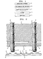
- FIG. 3 is a schematic cross section of an exemplary flat panel display 90 using the high breakdown voltage pillars according to the present invention.
- the display comprises a cathode 91 including a plurality of emitters 92 and an anode 93 disposed in spaced relation from the emitters within a vacuum seal.
- the anode conductor 93 formed on a transparent insulating substrate 94 is provided with a phosphor layer 95 and mounted on support pillars 96.
- a perforated conductive gate layer 97 Between the cathode and the anode and closely spaced from the emitters.
- the space between the anode and the emitter is sealed and evacuated, and voltage is applied by power supply 98.
- the field-emitted electrons from electron emitters 92 are accelerated by the gate electrode 97 from multiple emitters 92 on each pixel and move toward the anode conductive layer 93 (typically transparent conductor such as indium-tin-oxide) coated on the anode substrate 94.
- Phosphor layer 95 is disposed between the electron emitters and the anode. As the accelerated electrons hit the phosphor, a display image is generated.
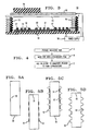
- FIG. 4 is a flow diagram illustrating the steps involved in a preferred method for creating a corrugated or grooved pillar rod structure.
- corrugated encompasses a grooved structure.
- the FIG. 4 method is based on additive processing.
- the corrugated structure is created by adding extra dielectric material, in a pre-designed fashion, on the surface of the rod, wire or plate-shaped base dielectric material.
- the term "rod” as used herein encompasses a cylinder, a vertically-oriented plate or any other aperiodic shape used as the base form for a pillar.
- the first step, block A in FIG. 4 is to provide a rod-shaped dielectric starting material.
- a long wire in the form of wound spool is a convenient configuration for handling.
- Optical fiber glass which is widely used for telecommunications, is easily available, relatively low-cost material with roughly right size and shape, and hence can conveniently be utilized.
- Other dielectric materials such as polymer wires or, ceramic wires can also be
- the next step in FIG. 4 is to apply a patterned, anti-adhesion film (or mask) on the surface of the base wire material, either circumferentially or helically.
- the anti-adhesion film is exemplarily made of a thin coating of wax, teflon or diamond, applied by any physical, chemical or electro-chemical deposition technique such as spray-coating or dip-coating. Rotation can advantageously be used to assist annular or helical deposition.
- the desired pitch of the circumferential or helix pattern is typically 10-100 ⁇ m for a pillar height of about 300-1000 ⁇ m.
- the patterning can be optionally aided by the use of known mask or photolithography procedures (e.g., exposing rotating wire to a beam of UV light).
- the next step is to add extra dielectric material to form annular or helical corrugations.
- This is accomplished, for example, by dip-coating, spray-coating, electrostatic, electrophoretic, or electrochemical deposition on the wire with a slurry, sol-gel precursor, melt, aqueous solution, or dry powder that contains either the dielectric material itself (e.g., powder) or a precursor of the dielectric (the same as the base wire or a different material).
- Continuously pulling wires through a liquid bath is an advantageous method.
- the patterned anti-adhesion film ensures the addition of material selectively where the film is not present.
- a slurry consisting of silica or glass particles with suitable binder and solvent may be coated on the base wire.
- a water glass (sodium silicate) solution or well-known sol-gel precursor for optical fiber glass may also be used.
- This process of adding the patterned dielectric material can be repeated if desired to increase the depth of the groove, with optional intermediate or final baking or firing to burn off binder and solvent, and cause strong bonding and densification.
- Glasses are typically fired at 500-1000°C for 0.1-100 hrs.
- Ceramics and quartz can be sintered or fused typically at 800-1200°C for 0.1-100 hrs.
- Water glass can be dried or baked at lower temperature of below ⁇ 500°C.
- the added patterned dielectric material is made of polymer-based liquid or slurry, polymerization or curing either by heat (typically below ⁇ 300°C or catalyst, or fusing (in the case of thermoplastic polymer) can be used to density the material. A careful selection of polymer is needed for the field emission device applications because of the possibility of outgassing in vacuum environment.
- the anti-adhesion film may be optionally dissolved off or burned off, leaving a corrugated pillar structure with increased surface length.
- FIGs. 5A, 5B, 5C and 5D illustrate the rod at various stages of fabrication.
- FIG. 5A shows the cylindrical rod or wire 50 at the outset.
- FIG. 5B illustrates the rod 50 with the anti-adhesion coating 51 in place.
- FIG. 5C shows the addition of dielectric corrugations 52 on the portions of rod 50 not covered with coating 51, and
- FIG. 5D shows the rod with corrugations 52 after the anti-adhesion coating is burned away.
- a thicker patterned photoresist mask can be employed in lieu of anti-adhesion coating 51.
- Photoresist patterning of deep grooved mask with an aspect ratio in excess of 1 is an established technique.
- the additional dielectric material is added into these deep grooves.
- Spray-coating, dip-coating, electrostatic or electrophoretic deposition of powders, slurry, sol-gel, melt or aqueous solution containing the desired dielectric material or its precursor can be used, followed by baking or sintering and optional dissolution or pyrolysis of the mask material.
- the deep-grooved dielectric pillar structure is particularly desirable because not only is the breakdown voltage raised, but the secondary emission electrons can be trapped in the deep groove for improved reliability of the pillar.
- the desired depth of the groove expressed in terms of the ratio of the groove depth d to the maximum width of the groove opening w, is at least d/w >0.3, and preferably d/w >1.0.
- FIG. 6 is a flow diagram for a second method of creating a corrugated (grooved) pillar structure, this method based on subtractive processing.
- the grooved structure in this case is produced by removing (e.g., by etching away) part of the dielectric material in a pre-designed fashion from the surface of the wire-shaped base dielectric material.
- the first step, block A in FIG. 6, is to provide a dielectric rod of starting material.
- the next step (block B) is to apply a peripherally patterned (e.g. annular or helical), etch-resistant film on the rod surface.
- a peripherally patterned (e.g. annular or helical), etch-resistant film on the rod surface.
- Photoresist polymer materials can be spray-coated or dip-coated and UV patterned.
- etch-resistant metal Au or Pt films on glass are relatively resistant to chemical etching by hydrofluoric acid
- ceramic films may be used. These films are physically (as by evaporation or sputtering) or chemically (as by electroless plating or chemical vapor deposition) deposited. They can be patterned either by deposition through a patterned template or by mechanical removal of local regions as by scribing with a sharp-tipped comb.
- FIG. 7A The rod at various stages of the FIG. 6 method is schematically illustrated in FIGs. 7A, 7B and 7C.
- the etch-resistant film 71 is applied with a desired helical or annular pattern on the surface of the dielectric rod 50, which is then etched (e.g., in HF acid in the case of glass wire, in NaOH in the case of aluminum oxide wire for a suitable time period to obtain etched regions 72 as shown in FIG. 7B.
- the remnant etch-resistant film 71 is then optionally dissolved, etched or burned off to leave a corrugated, grooved dielectric pillar structure of FIG. 7C.
- the desired depth of the groove is typically d/w >0.3 and preferably d/w >1.0.
- the shallower grooves have a generally lenticular shape.
- the deeper grooves have additional benefit of trapping secondary emission electrons for enhanced reliability of the pillar.
- FIG. 8 is a flow diagram for processing steps using plastic deformation for shaping the pillar.
- the first step in FIG. 8 (block A) is to provide a rod-shaped dielectric material.
- the second step (block B) is to soften the rod, as by applying heat.
- Lime glass and pyrex glass are softened at temperatures below ⁇ 900°C. Quartz is softened at > 1100°C.
- Thermoplastic wires are softened at a relatively low temperature of typically below ⁇ 500°C.
- the next step in FIG. 8 is to plastically deform the softened rod by mechanical compression with a corrugated die, usually consisting of mating pair, and preferably cooled so that undesirable adhesion between the die and wire is minimized.
- a corrugated die usually consisting of mating pair, and preferably cooled so that undesirable adhesion between the die and wire is minimized.
- One exemplary forming die comprising two halves 90A and 90B is schematically illustrated in FIG. 9. A portion of the rod 50 is deformed and moved lengthwise so that the next portion can be deformed.
- the above-described embodiments are illustrative of only a few of the many possible specific embodiments which can represent applications of the principles of the invention.
- the high breakdown voltage pillars of this invention can be used not only for flat-panel display apparatus but for other applications, such as a x-y matrix addressable electron sources for electron lithography or for microwave power amplifier tubes.
Abstract
Description
- This invention relates to methods for making field emission devices and, in particular, to methods for making field emission devices, such as flat panel displays, having corrugated support pillars for breakdown resistance.
- Support pillars are important components of electron field emission devices (FEDs) such as flat panel displays. A typical field emission device comprises a cathode including a plurality of field emitter tips and an anode spaced from the cathode. A voltage applied between the anode and cathode induces emission of electrons towards the anode. In flat panel displays an additional electrode called a gate is typically disposed between the anode and cathode to selectively activate desired pixels. The space between the cathode and anode is evacuated, and integrated cylindrical support pillars keep the cathode and anode separated. Without support pillars, the atmospheric pressure outside would force the anode and cathode surfaces together. Pillars are typically 100-1000 µm high and each provides pillar support for an area of 1-10,000 pixels.
- While cylindrical pillars may provide adequate mechanical support, they are not well suited for new field emission devices employing higher voltages. Applicants have determined that increasing the operating voltage between the emitting cathode and the anode can substantially increase the efficiency and operating life of a field emission device. For example, in a flat panel display, changing the operating voltage from 500 V to 5000 V could increase the operating life of a typical phosphor by a factor of 100. However, because of the close spacing between electrodes, insulator breakdown and arcing along the surface of cylindrical pillars precludes the use of such high voltages.
- If a cylindrical insulator is disposed between two electrodes and subjected to a continuous voltage gradient, then emitted electrons colliding with the dielectric can stimulate the emission of secondary electrons. These secondary electrons in turn accelerate toward the positive electrode. This secondary emission can lead to a runaway process where the insulator becomes positively charged and an arc forms along the surface. Accordingly, there is a need for a new pillar design that will permit the use of higher voltages without breakdown and arcing.
- A field emission device is made by providing the device electrodes, forming a plurality of corrugated insulating rods, adhering the rods to an electrode, cutting away the tops of the rods to define corrugated pillars, and finishing the device. The corrugated rods can be formed in one of three different methods. The result is low cost production of a field emission device having superior resistance to breakdown in high voltage operation.
- In the drawings:
- FIG. 1 is a schematic block diagram of the steps in making an electron field emission device according to the invention;
- FIG. 2 illustrates apparatus useful in practicing the method of FIG. 1.
- FIG. 3 illustrates an exemplary FED display made by the process of FIG. 1.
- FIG. 4 illustrates a first method for making corrugated rods used in the process of FIG. 1.
- FIG. 5A, 5B and 5C illustrate a rod at various stages of the FIG. 4 process.
- FIG. 6 illustrates a second method for making corrugated rods.
- FIG. 7A, 7B and 7C illustrate a rod at various stages of the FIG. 6 process.
- FIG. 8 illustrates a third method for making corrugated rods; and
- FIG. 9 illustrates apparatus useful in the FIG. 8 process.
- This description is divided into two parts. Part I describes fabrication of a FED device having corrugated support pillars and part II describes preferred ways of making the corrugated pillars.
- Referring to the drawings, FIG. 1 is a block diagram of the steps in making a field emission device. A preliminary step shown in Block A, is to provide the device electrodes: an emitter cathode and an anode which may include a phosphor layer. Preferably the emitter cathode uses diamond field emitters because of their low voltage emission and their robust mechanical and chemical properties. Field emitting cathodes employing diamond field emitters are described, for example, in Okano et al., Appl. Phys. Lett., Vol. 64, p. 2742 (1994) and in United States Patents Nos. 5,129,850 and 5,138,237, all of which are incorporated by reference. Preferred electrodes for flat panel displays are disclosed in co-pending United States Patent application Serial No. 08/220,077 filed by Eom et al. on March 30, 1994; and the following applications filed by Jin et al: Serial No. 08/299674 (August 31, 1994); Serial No. 08/299470 (August 31, 1994); Serial No. 08/331458 (October 31, 1994); Serial No. 08/332179 (October 31, 1994); and Serial No. 08/361616 (December 22, 1994).
- The next step (FIG. 1, Block B) is to form a plurality of corrugated insulating rods to be used as support pillars separating the emitter cathode from an anode.
- There are five considerations in optimal pillar design. First, the optimal pillar design is one where the height of the pillar is short in order to minimize the divergence of emitted electrons, while the length of surface paths from negative to positive electrodes are as long as possible in order to reduce the likelihood of insulator breakdown. Second, it is desirable to construct the pillar so that most secondary electrons will re-impact the pillar surface close to the point of their generation, rather than being accelerated a substantial distance toward the positive electrode. This goal is advantageous because most materials generate less than one secondary electron for each incident electron if the incident energy is less than 500V (or preferably, less than 200V). Under these conditions, secondary electrons will generally not have enough energy to make an increasing number of secondaries of their own. For the purposes of this goal, "close" is defined as a point where the electrostatic potential is less than 500V more positive than the point at which the electron is generated, and preferably less than 200V more positive. Third, it is desirable to construct the pillar out of dielectric materials that have secondary electron emission coefficients of less than two, under the normal operating conditions. Fourth, it is desirable to have as much of the surface of the pillar oriented so that the local electric field is nearly normal to the insulator surface, preferably with the field lines emerging from the surface, so that secondary electrons will be pulled back toward the surface and re-impact with energies less than the abovementioned 200-500V. Fifth, the pillar must not be so much wider at the anode end so that it substantially reduces the area that can be allocated to the phosphor screen.
- Where the field emission device is a flat panel display, the pillar material should not only be mechanically strong but also should be an electrical insulator with a high breakdown voltage in order to withstand the high electrical field applied to operate the phosphor of the display. For established phosphors such as ZnS:Cu, Al, the breakdown voltage should be greater than about 2000 V and preferably greater than 4000 V.
- A suitable pillar material may be chosen from glasses such as lime glass, pyrex, fused quartz, ceramic materials such as oxide, nitride, oxynitride, carbide (e.g., Al2O3, TiO2, ZrO2, AlN), polymers (e.g., polyimide resins) or composites of ceramics, polymers, or metals.
- A typical geometry of the pillar is advantageously a modified form of either round or rectangular rod. The diameter or thickness of the pillar is typically 50-1000 µm, and preferably 100-300 µm. The height-to-diameter or height-to-thickness aspect ratio of the pillar is typically in the range of 1-10, preferably in the range of 3-6. The desired number or density of the pillars is dependent on various factors to be considered. For sufficient mechanical support of the anode plate, a larger number of pillars is desirable, however, in order to minimize expense, electrical leakage, and the possibility of breakdown, some compromise is necessary. A typical density of the pillar is about 0.01-2% of the total display surface area, and preferably 0.05-0.5%. A FED display of about 25x25 cm2 area with approximately 500-100,000 pillars, each with a cross-sectional area of 100x100 µm2 is a good example.
- Since the breakdown of the dielectric properties in the pillar occurs most frequently at its surface, it is desirable to increase the surface length of the pillar between the cathode and the anode. The surface distance is increased by introducing corrugations --either annular or helical-- in the pillar rod. The corrugations are advantageously formed in one of three ways described hereinafter in Part II.
- After the corrugated rods are formed, the next step shown in FIG. 1, block C, is to adhere the ends of a plurality of rods to an electrode (either cathode or anode) of the field emitting device, preferably the emitting cathode. The placement of pillars on the electrode can be conveniently accomplished by using the apparatus illustrated in FIG. 2. Specifically, a plurality of
corrugated rods 20 are applied to anelectrode 21 through apertures in a two part template comprising anupper portion 23 and alower portion 24. In the insertion phase, theapertures electrode 21.Notches 28 are advantageously provided in the rods at desired cutting points. In the example shown, the electrode is the device cathode emitter includingemitter regions 10 onconductive substrate 21.Conductive gates 11 are separated from the substrate by an insulatinglayer 12. - For a FED display requiring 1000 pillars, for example, display--sized templates (e.g., metal sheets with drilled holes at the desired pillar locations), are first prepared. The template holes are simultaneously and continuously supplied with long rods (wires) of corrugated dielectric material. The protruding bottoms of the wires are coated with a material to facilitate bonding, such as adhesive material (e.g. uncured or semicured epoxy), low melting point glass or solder that is molten or in the paste form. Adhesion can be facilitated, if necessary, by locally heating the pillar-to-electrode junction by a laser beam.
- The next step shown in Block D of FIG. 1 is to cut the corrugated rods into support pillars. This can be advantageously done by shearing with the apparatus of FIG. 2. The
upper template 23 is moved sideways while thelower template 24 is fixed with the adhesive in contact with display cathode surface, so that the bottom pillar is broken away at the pre-designed V-notch location 28. This process is repeated for the next display substrate. As many of the pillars are placed simultaneously, the assembly can be fast and of low cost. - The final step of FIG. 1 Block E is to finish the device by applying the other electrode and evacuating the space between the two electrodes. The preferred use of these corrugated pillars is in the fabrication of field emission devices such as electron emission flat panel displays. FIG. 3 is a schematic cross section of an exemplary
flat panel display 90 using the high breakdown voltage pillars according to the present invention. The display comprises acathode 91 including a plurality ofemitters 92 and ananode 93 disposed in spaced relation from the emitters within a vacuum seal. Theanode conductor 93 formed on a transparent insulatingsubstrate 94 is provided with aphosphor layer 95 and mounted onsupport pillars 96. Between the cathode and the anode and closely spaced from the emitters is a perforatedconductive gate layer 97. - The space between the anode and the emitter is sealed and evacuated, and voltage is applied by
power supply 98. The field-emitted electrons fromelectron emitters 92 are accelerated by thegate electrode 97 frommultiple emitters 92 on each pixel and move toward the anode conductive layer 93 (typically transparent conductor such as indium-tin-oxide) coated on theanode substrate 94.Phosphor layer 95 is disposed between the electron emitters and the anode. As the accelerated electrons hit the phosphor, a display image is generated. - FIG. 4 is a flow diagram illustrating the steps involved in a preferred method for creating a corrugated or grooved pillar rod structure. As used herein, the term "corrugated" encompasses a grooved structure. The FIG. 4 method is based on additive processing. The corrugated structure is created by adding extra dielectric material, in a pre-designed fashion, on the surface of the rod, wire or plate-shaped base dielectric material. The term "rod" as used herein encompasses a cylinder, a vertically-oriented plate or any other aperiodic shape used as the base form for a pillar. The first step, block A in FIG. 4, is to provide a rod-shaped dielectric starting material. A long wire in the form of wound spool is a convenient configuration for handling. Optical fiber glass, which is widely used for telecommunications, is easily available, relatively low-cost material with roughly right size and shape, and hence can conveniently be utilized. Other dielectric materials such as polymer wires or, ceramic wires can also be used.
- The next step in FIG. 4 (block B) is to apply a patterned, anti-adhesion film (or mask) on the surface of the base wire material, either circumferentially or helically. The anti-adhesion film is exemplarily made of a thin coating of wax, teflon or diamond, applied by any physical, chemical or electro-chemical deposition technique such as spray-coating or dip-coating. Rotation can advantageously be used to assist annular or helical deposition. The desired pitch of the circumferential or helix pattern is typically 10-100 µm for a pillar height of about 300-1000 µm. The patterning can be optionally aided by the use of known mask or photolithography procedures (e.g., exposing rotating wire to a beam of UV light).
- The next step (block C in FIG. 4) is to add extra dielectric material to form annular or helical corrugations. This is accomplished, for example, by dip-coating, spray-coating, electrostatic, electrophoretic, or electrochemical deposition on the wire with a slurry, sol-gel precursor, melt, aqueous solution, or dry powder that contains either the dielectric material itself (e.g., powder) or a precursor of the dielectric (the same as the base wire or a different material). Continuously pulling wires through a liquid bath is an advantageous method. The patterned anti-adhesion film ensures the addition of material selectively where the film is not present. A slurry consisting of silica or glass particles with suitable binder and solvent may be coated on the base wire. A water glass (sodium silicate) solution or well-known sol-gel precursor for optical fiber glass may also be used. This process of adding the patterned dielectric material can be repeated if desired to increase the depth of the groove, with optional intermediate or final baking or firing to burn off binder and solvent, and cause strong bonding and densification. Glasses are typically fired at 500-1000°C for 0.1-100 hrs. Ceramics and quartz can be sintered or fused typically at 800-1200°C for 0.1-100 hrs. Water glass can be dried or baked at lower temperature of below ∼500°C. If the added patterned dielectric material is made of polymer-based liquid or slurry, polymerization or curing either by heat (typically below ∼300°C or catalyst, or fusing (in the case of thermoplastic polymer) can be used to density the material. A careful selection of polymer is needed for the field emission device applications because of the possibility of outgassing in vacuum environment. After the added dielectric coating is solidified and adhered to the base wire, the anti-adhesion film may be optionally dissolved off or burned off, leaving a corrugated pillar structure with increased surface length.
- FIGs. 5A, 5B, 5C and 5D illustrate the rod at various stages of fabrication. FIG. 5A shows the cylindrical rod or
wire 50 at the outset. FIG. 5B illustrates therod 50 with theanti-adhesion coating 51 in place. FIG. 5C shows the addition ofdielectric corrugations 52 on the portions ofrod 50 not covered withcoating 51, and FIG. 5D shows the rod withcorrugations 52 after the anti-adhesion coating is burned away. - If a deeper groove structure is desired in order to further increase the surface length on the pillar and raise the breakdown voltage, a thicker patterned photoresist mask can be employed in lieu of
anti-adhesion coating 51. Photoresist patterning of deep grooved mask with an aspect ratio in excess of 1 is an established technique. The additional dielectric material is added into these deep grooves. Spray-coating, dip-coating, electrostatic or electrophoretic deposition of powders, slurry, sol-gel, melt or aqueous solution containing the desired dielectric material or its precursor can be used, followed by baking or sintering and optional dissolution or pyrolysis of the mask material. The deep-grooved dielectric pillar structure is particularly desirable because not only is the breakdown voltage raised, but the secondary emission electrons can be trapped in the deep groove for improved reliability of the pillar. The desired depth of the groove expressed in terms of the ratio of the groove depth d to the maximum width of the groove opening w, is at least d/w >0.3, and preferably d/w >1.0. - FIG. 6 is a flow diagram for a second method of creating a corrugated (grooved) pillar structure, this method based on subtractive processing. The grooved structure in this case is produced by removing (e.g., by etching away) part of the dielectric material in a pre-designed fashion from the surface of the wire-shaped base dielectric material. The first step, block A in FIG. 6, is to provide a dielectric rod of starting material.
- The next step (block B) is to apply a peripherally patterned (e.g. annular or helical), etch-resistant film on the rod surface. Photoresist polymer materials, can be spray-coated or dip-coated and UV patterned. Alternatively, etch-resistant metal (Au or Pt films on glass are relatively resistant to chemical etching by hydrofluoric acid) or ceramic films may be used. These films are physically (as by evaporation or sputtering) or chemically (as by electroless plating or chemical vapor deposition) deposited. They can be patterned either by deposition through a patterned template or by mechanical removal of local regions as by scribing with a sharp-tipped comb.
- The rod at various stages of the FIG. 6 method is schematically illustrated in FIGs. 7A, 7B and 7C. In FIG. 7A, the etch-
resistant film 71 is applied with a desired helical or annular pattern on the surface of thedielectric rod 50, which is then etched (e.g., in HF acid in the case of glass wire, in NaOH in the case of aluminum oxide wire for a suitable time period to obtainetched regions 72 as shown in FIG. 7B. The remnant etch-resistant film 71 is then optionally dissolved, etched or burned off to leave a corrugated, grooved dielectric pillar structure of FIG. 7C. The desired depth of the groove is typically d/w >0.3 and preferably d/w >1.0. The shallower grooves have a generally lenticular shape. The deeper grooves have additional benefit of trapping secondary emission electrons for enhanced reliability of the pillar. - Yet another approach to creating the desired corrugated pillar structure is based on shaping the pillar using predesigned moulds. FIG. 8 is a flow diagram for processing steps using plastic deformation for shaping the pillar. The first step in FIG. 8 (block A) is to provide a rod-shaped dielectric material.
- The second step (block B) is to soften the rod, as by applying heat. Lime glass and pyrex glass are softened at temperatures below ∼900°C. Quartz is softened at > 1100°C. Thermoplastic wires are softened at a relatively low temperature of typically below ∼500°C.
- The next step in FIG. 8 is to plastically deform the softened rod by mechanical compression with a corrugated die, usually consisting of mating pair, and preferably cooled so that undesirable adhesion between the die and wire is minimized. One exemplary forming die comprising two
halves rod 50 is deformed and moved lengthwise so that the next portion can be deformed. - It is to be understood that the above-described embodiments are illustrative of only a few of the many possible specific embodiments which can represent applications of the principles of the invention. For example, the high breakdown voltage pillars of this invention can be used not only for flat-panel display apparatus but for other applications, such as a x-y matrix addressable electron sources for electron lithography or for microwave power amplifier tubes.
Claims (11)
- A method for making a field emission device comprising an emitter cathode electrode and an anode electrode spaced apart by a plurality of dielectric pillars comprising the steps of:providing said electrodes;forming a plurality of corrugated dielectric rods;adhering said rods to one of said electrodes;cutting said rods; andfinishing said device.
- The method of claim 1 wherein said corrugated insulating rods are formed by providing dielectric rods, masking portions of said rods with anti-adhesion film, and adding dielectric material to unmasked regions on said rods to form corrugations.
- The method of claim 1 wherein said corrugated insulating rods are formed by providing dielectric rods, masking portions of said rods with etch-resistant film, and etching dielectric material from unmasked regions on said rods to form corrugations.
- The method of claim 1 wherein said corrugated insulating rods are formed by providing dielectric rods, softening said rods, and deforming the rods to mold corrugations.
- The method of claim 1 wherein said rods are adhered to said emitter cathode electrode.
- The method of claim 1 wherein said step of adhering said rods to one of said electrodes includes the step of passing said rods through apertures in a template into contact with said electrode.
- The method of claim 1 wherein said step of cutting said rods comprises passing said rods through apertures in a two-part template and shearing said rods between the two ports of said template.
- In an electron field emission device comprising an emitter cathode, and anode and a plurality of insulating pilars spacing apart said cathode and anode, the improvement wherein:at least one of said insulating pillars has a corrugated outer surface for reducing arcing between said cathode and anode along the surface of said pillar.
- The improved device of claim 8 wherein the corrugations of said pillar are grooves having depth d and maximum width of groove opening w and d/w > 0.3, or > 1.0.
- The improved device of claim 8, wherein said insulating pillars are glass fibers.
- The improved device of claim 8, wherein said corrugations are either helical, or annular.
Applications Claiming Priority (2)
| Application Number | Priority Date | Filing Date | Title |
|---|---|---|---|
| US08/381,262 US5561340A (en) | 1995-01-31 | 1995-01-31 | Field emission display having corrugated support pillars and method for manufacturing |
| US381262 | 1995-01-31 |
Publications (2)
| Publication Number | Publication Date |
|---|---|
| EP0725419A1 true EP0725419A1 (en) | 1996-08-07 |
| EP0725419B1 EP0725419B1 (en) | 2000-06-07 |
Family
ID=23504338
Family Applications (1)
| Application Number | Title | Priority Date | Filing Date |
|---|---|---|---|
| EP96300483A Revoked EP0725419B1 (en) | 1995-01-31 | 1996-01-24 | Method for making field emission devices having corrugated support pillars for breakdown resistance |
Country Status (5)
| Country | Link |
|---|---|
| US (1) | US5561340A (en) |
| EP (1) | EP0725419B1 (en) |
| JP (1) | JP2968201B2 (en) |
| CA (1) | CA2166505C (en) |
| DE (1) | DE69608713T2 (en) |
Cited By (4)
| Publication number | Priority date | Publication date | Assignee | Title |
|---|---|---|---|---|
| EP1032014A2 (en) | 1999-02-25 | 2000-08-30 | Canon Kabushiki Kaisha | Manufacturing method of spacer for electron-beam apparatus and manufacturing method of electron-beam apparatus |
| US6517399B1 (en) | 1998-09-21 | 2003-02-11 | Canon Kabushiki Kaisha | Method of manufacturing spacer, method of manufacturing image forming apparatus using spacer, and apparatus for manufacturing spacer |
| US6761606B2 (en) | 2000-09-08 | 2004-07-13 | Canon Kabushiki Kaisha | Method of producing spacer and method of manufacturing image forming apparatus |
| EP1517359A2 (en) * | 2003-09-17 | 2005-03-23 | Patent-Treuhand-Gesellschaft für elektrische Glühlampen mbH | Method of manufacturing of a flat discharge lamp with spacer elements |
Families Citing this family (22)
| Publication number | Priority date | Publication date | Assignee | Title |
|---|---|---|---|---|
| GB2280924B (en) * | 1993-08-10 | 1997-02-26 | Brian See | Structural members |
| CA2166506C (en) * | 1995-01-31 | 2000-11-28 | Sungho Jin | Improved field emission devices having corrugated support pillars with discontinuous conductive coating |
| US5704820A (en) * | 1995-01-31 | 1998-01-06 | Lucent Technologies Inc. | Method for making improved pillar structure for field emission devices |
| JP2809129B2 (en) * | 1995-04-20 | 1998-10-08 | 日本電気株式会社 | Field emission cold cathode and display device using the same |
| JP2907080B2 (en) * | 1995-09-26 | 1999-06-21 | 双葉電子工業株式会社 | Field emission display |
| JP3765901B2 (en) * | 1996-02-26 | 2006-04-12 | 株式会社東芝 | Plasma display and plasma liquid crystal display |
| EP0851458A1 (en) * | 1996-12-26 | 1998-07-01 | Canon Kabushiki Kaisha | A spacer and an image-forming apparatus, and a manufacturing method thereof |
| US5980349A (en) | 1997-05-14 | 1999-11-09 | Micron Technology, Inc. | Anodically-bonded elements for flat panel displays |
| US6554671B1 (en) * | 1997-05-14 | 2003-04-29 | Micron Technology, Inc. | Method of anodically bonding elements for flat panel displays |
| US6072274A (en) * | 1997-10-22 | 2000-06-06 | Hewlett-Packard Company | Molded plastic panel for flat panel displays |
| US6506087B1 (en) | 1998-05-01 | 2003-01-14 | Canon Kabushiki Kaisha | Method and manufacturing an image forming apparatus having improved spacers |
| EP1137041B1 (en) * | 1998-09-08 | 2011-04-06 | Canon Kabushiki Kaisha | Electron beam device, method for producing charging-suppressing member used in the electron beam device, and image forming device |
| JP4115051B2 (en) * | 1998-10-07 | 2008-07-09 | キヤノン株式会社 | Electron beam equipment |
| US6507146B2 (en) * | 2000-03-01 | 2003-01-14 | Chad Byron Moore | Fiber-based field emission display |
| GB0015928D0 (en) * | 2000-06-30 | 2000-08-23 | Printable Field Emitters Limit | Field emitters |
| US6670629B1 (en) | 2002-09-06 | 2003-12-30 | Ge Medical Systems Global Technology Company, Llc | Insulated gate field emitter array |
| JP3867065B2 (en) * | 2002-11-29 | 2007-01-10 | 日本碍子株式会社 | Electron emitting device and light emitting device |
| US7187114B2 (en) * | 2002-11-29 | 2007-03-06 | Ngk Insulators, Ltd. | Electron emitter comprising emitter section made of dielectric material |
| US7129642B2 (en) * | 2002-11-29 | 2006-10-31 | Ngk Insulators, Ltd. | Electron emitting method of electron emitter |
| US6750470B1 (en) | 2002-12-12 | 2004-06-15 | General Electric Company | Robust field emitter array design |
| US20040113178A1 (en) * | 2002-12-12 | 2004-06-17 | Colin Wilson | Fused gate field emitter |
| JP6526641B2 (en) * | 2013-06-21 | 2019-06-05 | スミスズ ディテクション モントリオール インコーポレイティド | Method and apparatus for coated corona ionization source |
Citations (3)
| Publication number | Priority date | Publication date | Assignee | Title |
|---|---|---|---|---|
| JPH02299136A (en) * | 1989-05-15 | 1990-12-11 | Canon Inc | Image forming device |
| EP0404022A2 (en) * | 1989-06-19 | 1990-12-27 | Matsushita Electric Industrial Co., Ltd. | Flat configuration image display apparatus and manufacturing method thereof |
| EP0616354A2 (en) * | 1993-03-18 | 1994-09-21 | International Business Machines Corporation | Spacers for flat panel displays |
Family Cites Families (6)
| Publication number | Priority date | Publication date | Assignee | Title |
|---|---|---|---|---|
| US3665241A (en) * | 1970-07-13 | 1972-05-23 | Stanford Research Inst | Field ionizer and field emission cathode structures and methods of production |
| FR2623013A1 (en) * | 1987-11-06 | 1989-05-12 | Commissariat Energie Atomique | ELECTRO SOURCE WITH EMISSIVE MICROPOINT CATHODES AND FIELD EMISSION-INDUCED CATHODOLUMINESCENCE VISUALIZATION DEVICE USING THE SOURCE |
| US5063327A (en) * | 1988-07-06 | 1991-11-05 | Coloray Display Corporation | Field emission cathode based flat panel display having polyimide spacers |
| US5129850A (en) * | 1991-08-20 | 1992-07-14 | Motorola, Inc. | Method of making a molded field emission electron emitter employing a diamond coating |
| US5138237A (en) * | 1991-08-20 | 1992-08-11 | Motorola, Inc. | Field emission electron device employing a modulatable diamond semiconductor emitter |
| US5283500A (en) * | 1992-05-28 | 1994-02-01 | At&T Bell Laboratories | Flat panel field emission display apparatus |
-
1995
- 1995-01-31 US US08/381,262 patent/US5561340A/en not_active Expired - Lifetime
-
1996
- 1996-01-03 CA CA002166505A patent/CA2166505C/en not_active Expired - Fee Related
- 1996-01-24 EP EP96300483A patent/EP0725419B1/en not_active Revoked
- 1996-01-24 DE DE69608713T patent/DE69608713T2/en not_active Expired - Fee Related
- 1996-01-29 JP JP8012720A patent/JP2968201B2/en not_active Expired - Lifetime
Patent Citations (3)
| Publication number | Priority date | Publication date | Assignee | Title |
|---|---|---|---|---|
| JPH02299136A (en) * | 1989-05-15 | 1990-12-11 | Canon Inc | Image forming device |
| EP0404022A2 (en) * | 1989-06-19 | 1990-12-27 | Matsushita Electric Industrial Co., Ltd. | Flat configuration image display apparatus and manufacturing method thereof |
| EP0616354A2 (en) * | 1993-03-18 | 1994-09-21 | International Business Machines Corporation | Spacers for flat panel displays |
Non-Patent Citations (1)
| Title |
|---|
| PATENT ABSTRACTS OF JAPAN vol. 015, no. 082 (E - 1038) 26 February 1991 (1991-02-26) * |
Cited By (7)
| Publication number | Priority date | Publication date | Assignee | Title |
|---|---|---|---|---|
| US6517399B1 (en) | 1998-09-21 | 2003-02-11 | Canon Kabushiki Kaisha | Method of manufacturing spacer, method of manufacturing image forming apparatus using spacer, and apparatus for manufacturing spacer |
| US6926571B2 (en) | 1998-09-21 | 2005-08-09 | Canon Kabushiki Kaisha | Method of manufacturing spacer, method of manufacturing image forming apparatus using spacer, and apparatus for manufacturing spacer |
| EP1032014A2 (en) | 1999-02-25 | 2000-08-30 | Canon Kabushiki Kaisha | Manufacturing method of spacer for electron-beam apparatus and manufacturing method of electron-beam apparatus |
| EP1032014A3 (en) * | 1999-02-25 | 2007-06-20 | Canon Kabushiki Kaisha | Manufacturing method of spacer for electron-beam apparatus and manufacturing method of electron-beam apparatus |
| US6761606B2 (en) | 2000-09-08 | 2004-07-13 | Canon Kabushiki Kaisha | Method of producing spacer and method of manufacturing image forming apparatus |
| EP1517359A2 (en) * | 2003-09-17 | 2005-03-23 | Patent-Treuhand-Gesellschaft für elektrische Glühlampen mbH | Method of manufacturing of a flat discharge lamp with spacer elements |
| EP1517359A3 (en) * | 2003-09-17 | 2006-06-14 | Patent-Treuhand-Gesellschaft für elektrische Glühlampen mbH | Method of manufacturing of a flat discharge lamp with spacer elements |
Also Published As
| Publication number | Publication date |
|---|---|
| DE69608713D1 (en) | 2000-07-13 |
| JP2968201B2 (en) | 1999-10-25 |
| CA2166505A1 (en) | 1996-08-01 |
| JPH08241670A (en) | 1996-09-17 |
| CA2166505C (en) | 2001-03-20 |
| DE69608713T2 (en) | 2000-11-09 |
| US5561340A (en) | 1996-10-01 |
| EP0725419B1 (en) | 2000-06-07 |
Similar Documents
| Publication | Publication Date | Title |
|---|---|---|
| EP0725419B1 (en) | Method for making field emission devices having corrugated support pillars for breakdown resistance | |
| CA2166504C (en) | Multilayer pillar structure for improved field emission devices | |
| US20060246295A1 (en) | Thick-film sheet member, devices to which the sheet member is applied, and methods of producing the sheet member and the devices | |
| US7365482B2 (en) | Field emission display including electron emission source formed in multi-layer structure | |
| KR100602071B1 (en) | Field emission devices | |
| EP1553613B1 (en) | Method of forming carbon nanotube emitter | |
| CA2168377C (en) | Method for making improved pillar structure for field emission devices | |
| EP0725418B1 (en) | Field emission devices having corrugated support pillars with discontinuous conductive coating | |
| JP3836539B2 (en) | Field emission device and manufacturing method thereof | |
| US20050136178A1 (en) | Method and apparatus for producing microchannel plate using corrugated mold | |
| CN1282448A (en) | Field emission device having composite spacer | |
| CN1784763A (en) | Image display device and manufacturing method for spacer assembly used in image display device | |
| KR100326532B1 (en) | Method of Fabricating A Spacer Member For Flat Display Panel | |
| KR100303546B1 (en) | Field emission display and manufacturing method of the same | |
| JP2003059391A (en) | Electron emitting source and method of its manufacture and fluorescent character display device | |
| EP0470631A2 (en) | Wire shaped electron source | |
| KR100351149B1 (en) | Manufacturing method for display | |
| KR100266224B1 (en) | Field emission device and the manufacturing method thereof and field emission display using it | |
| KR100261542B1 (en) | A method for manufacturing spacer of a field effect electron emission device | |
| KR20050112175A (en) | Process for manufacturing electron emission device without activation step of electron emission source | |
| JPS61138427A (en) | Manufacture of vacuum fluorescent display device |
Legal Events
| Date | Code | Title | Description |
|---|---|---|---|
| PUAI | Public reference made under article 153(3) epc to a published international application that has entered the european phase |
Free format text: ORIGINAL CODE: 0009012 |
|
| AK | Designated contracting states |
Kind code of ref document: A1 Designated state(s): DE FR GB |
|
| 17P | Request for examination filed |
Effective date: 19970122 |
|
| 17Q | First examination report despatched |
Effective date: 19970228 |
|
| GRAG | Despatch of communication of intention to grant |
Free format text: ORIGINAL CODE: EPIDOS AGRA |
|
| GRAG | Despatch of communication of intention to grant |
Free format text: ORIGINAL CODE: EPIDOS AGRA |
|
| GRAH | Despatch of communication of intention to grant a patent |
Free format text: ORIGINAL CODE: EPIDOS IGRA |
|
| GRAH | Despatch of communication of intention to grant a patent |
Free format text: ORIGINAL CODE: EPIDOS IGRA |
|
| GRAA | (expected) grant |
Free format text: ORIGINAL CODE: 0009210 |
|
| AK | Designated contracting states |
Kind code of ref document: B1 Designated state(s): DE FR GB |
|
| REF | Corresponds to: |
Ref document number: 69608713 Country of ref document: DE Date of ref document: 20000713 |
|
| ET | Fr: translation filed | ||
| PG25 | Lapsed in a contracting state [announced via postgrant information from national office to epo] |
Ref country code: GB Free format text: LAPSE BECAUSE OF NON-PAYMENT OF DUE FEES Effective date: 20010124 |
|
| PLBQ | Unpublished change to opponent data |
Free format text: ORIGINAL CODE: EPIDOS OPPO |
|
| PLBI | Opposition filed |
Free format text: ORIGINAL CODE: 0009260 |
|
| 26 | Opposition filed |
Opponent name: CANON KABUSHIKI KAISHA Effective date: 20010308 |
|
| GBPC | Gb: european patent ceased through non-payment of renewal fee |
Effective date: 20010124 |
|
| PG25 | Lapsed in a contracting state [announced via postgrant information from national office to epo] |
Ref country code: FR Free format text: LAPSE BECAUSE OF NON-PAYMENT OF DUE FEES Effective date: 20010928 |
|
| PG25 | Lapsed in a contracting state [announced via postgrant information from national office to epo] |
Ref country code: DE Free format text: LAPSE BECAUSE OF NON-PAYMENT OF DUE FEES Effective date: 20011101 |
|
| REG | Reference to a national code |
Ref country code: FR Ref legal event code: ST |
|
| RDAH | Patent revoked |
Free format text: ORIGINAL CODE: EPIDOS REVO |
|
| RDAG | Patent revoked |
Free format text: ORIGINAL CODE: 0009271 |
|
| STAA | Information on the status of an ep patent application or granted ep patent |
Free format text: STATUS: PATENT REVOKED |
|
| 27W | Patent revoked |
Effective date: 20020523 |