EP0724221A2 - Verfahren und Vorrichtung zur Ausführung unähnlicher Befehlsfolgen in einem Prozessor eines Einzelbefehl- und Mehrfahrdatenrechners (SIMD) - Google Patents
Verfahren und Vorrichtung zur Ausführung unähnlicher Befehlsfolgen in einem Prozessor eines Einzelbefehl- und Mehrfahrdatenrechners (SIMD) Download PDFInfo
- Publication number
- EP0724221A2 EP0724221A2 EP95112674A EP95112674A EP0724221A2 EP 0724221 A2 EP0724221 A2 EP 0724221A2 EP 95112674 A EP95112674 A EP 95112674A EP 95112674 A EP95112674 A EP 95112674A EP 0724221 A2 EP0724221 A2 EP 0724221A2
- Authority
- EP
- European Patent Office
- Prior art keywords
- instruction
- memory
- output
- register
- receiving
- Prior art date
- Legal status (The legal status is an assumption and is not a legal conclusion. Google has not performed a legal analysis and makes no representation as to the accuracy of the status listed.)
- Withdrawn
Links
Images


Classifications
-
- G—PHYSICS
- G06—COMPUTING OR CALCULATING; COUNTING
- G06F—ELECTRIC DIGITAL DATA PROCESSING
- G06F9/00—Arrangements for program control, e.g. control units
- G06F9/06—Arrangements for program control, e.g. control units using stored programs, i.e. using an internal store of processing equipment to receive or retain programs
- G06F9/30—Arrangements for executing machine instructions, e.g. instruction decode
- G06F9/30003—Arrangements for executing specific machine instructions
- G06F9/3004—Arrangements for executing specific machine instructions to perform operations on memory
- G06F9/30043—LOAD or STORE instructions; Clear instruction
-
- G—PHYSICS
- G06—COMPUTING OR CALCULATING; COUNTING
- G06F—ELECTRIC DIGITAL DATA PROCESSING
- G06F15/00—Digital computers in general; Data processing equipment in general
- G06F15/76—Architectures of general purpose stored program computers
- G06F15/80—Architectures of general purpose stored program computers comprising an array of processing units with common control, e.g. single instruction multiple data processors
- G06F15/8007—Architectures of general purpose stored program computers comprising an array of processing units with common control, e.g. single instruction multiple data processors single instruction multiple data [SIMD] multiprocessors
-
- G—PHYSICS
- G06—COMPUTING OR CALCULATING; COUNTING
- G06F—ELECTRIC DIGITAL DATA PROCESSING
- G06F9/00—Arrangements for program control, e.g. control units
- G06F9/06—Arrangements for program control, e.g. control units using stored programs, i.e. using an internal store of processing equipment to receive or retain programs
- G06F9/30—Arrangements for executing machine instructions, e.g. instruction decode
- G06F9/30145—Instruction analysis, e.g. decoding, instruction word fields
- G06F9/3016—Decoding the operand specifier, e.g. specifier format
- G06F9/30167—Decoding the operand specifier, e.g. specifier format of immediate specifier, e.g. constants
-
- G—PHYSICS
- G06—COMPUTING OR CALCULATING; COUNTING
- G06F—ELECTRIC DIGITAL DATA PROCESSING
- G06F9/00—Arrangements for program control, e.g. control units
- G06F9/06—Arrangements for program control, e.g. control units using stored programs, i.e. using an internal store of processing equipment to receive or retain programs
- G06F9/30—Arrangements for executing machine instructions, e.g. instruction decode
- G06F9/30181—Instruction operation extension or modification
- G06F9/30185—Instruction operation extension or modification according to one or more bits in the instruction, e.g. prefix, sub-opcode
-
- G—PHYSICS
- G06—COMPUTING OR CALCULATING; COUNTING
- G06F—ELECTRIC DIGITAL DATA PROCESSING
- G06F9/00—Arrangements for program control, e.g. control units
- G06F9/06—Arrangements for program control, e.g. control units using stored programs, i.e. using an internal store of processing equipment to receive or retain programs
- G06F9/30—Arrangements for executing machine instructions, e.g. instruction decode
- G06F9/30181—Instruction operation extension or modification
- G06F9/30189—Instruction operation extension or modification according to execution mode, e.g. mode flag
-
- G—PHYSICS
- G06—COMPUTING OR CALCULATING; COUNTING
- G06F—ELECTRIC DIGITAL DATA PROCESSING
- G06F9/00—Arrangements for program control, e.g. control units
- G06F9/06—Arrangements for program control, e.g. control units using stored programs, i.e. using an internal store of processing equipment to receive or retain programs
- G06F9/30—Arrangements for executing machine instructions, e.g. instruction decode
- G06F9/38—Concurrent instruction execution, e.g. pipeline or look ahead
- G06F9/3802—Instruction prefetching
-
- G—PHYSICS
- G06—COMPUTING OR CALCULATING; COUNTING
- G06F—ELECTRIC DIGITAL DATA PROCESSING
- G06F9/00—Arrangements for program control, e.g. control units
- G06F9/06—Arrangements for program control, e.g. control units using stored programs, i.e. using an internal store of processing equipment to receive or retain programs
- G06F9/30—Arrangements for executing machine instructions, e.g. instruction decode
- G06F9/38—Concurrent instruction execution, e.g. pipeline or look ahead
- G06F9/3885—Concurrent instruction execution, e.g. pipeline or look ahead using a plurality of independent parallel functional units
- G06F9/3887—Concurrent instruction execution, e.g. pipeline or look ahead using a plurality of independent parallel functional units controlled by a single instruction for multiple data lanes [SIMD]
-
- G—PHYSICS
- G06—COMPUTING OR CALCULATING; COUNTING
- G06F—ELECTRIC DIGITAL DATA PROCESSING
- G06F9/00—Arrangements for program control, e.g. control units
- G06F9/06—Arrangements for program control, e.g. control units using stored programs, i.e. using an internal store of processing equipment to receive or retain programs
- G06F9/30—Arrangements for executing machine instructions, e.g. instruction decode
- G06F9/38—Concurrent instruction execution, e.g. pipeline or look ahead
- G06F9/3885—Concurrent instruction execution, e.g. pipeline or look ahead using a plurality of independent parallel functional units
- G06F9/3889—Concurrent instruction execution, e.g. pipeline or look ahead using a plurality of independent parallel functional units controlled by multiple instructions, e.g. MIMD, decoupled access or execute
Definitions
- the present invention generally relates to single-instructionstream-multiple-data stream (SIMD) machines having a plurality of processing elements (PE) and a unique device therein in which efficiency of the machines is maintained even when executing different instructions in different PEs.
- SIMD single-instructionstream-multiple-data stream
- the present invention relates to a method and apparatus in which a local instruction buffer or a local instruction memory is utilized, thereby allowing the applicability of SIMD machines to be extended to a much larger set of applications.
- a SIMD computer includes a plurality of processing elements each of which has a local instruction source, a multiplexor, and means for modifying the broadcast instruction to execute dissimilar sequences of instructions.
- the present invention is directed to allowing different processors to execute different instructions, depending on their logical index or data content.
- parallel processing is widely regarded as the most promising approach for achieving the performance improvements essential for solving the most challenging scientific/engineering problems such as image processing, weather forecasting, nuclear-reactor calculations, pattern recognition and ballistic missile defense.
- parallel processors include a series of processing elements (PEs) each having data memories and operand registers and each of the PEs being interconnected through an interconnection network.
- PEs processing elements
- SIMD Single-Instruction-Stream-Multiple-Data-Stream
- MIMD Multiple-Instruction-Stream-Multiple-Data Stream
- SIMD includes a large number of processing elements having private data memories and arithmetic logic units (ALUs) which simultaneously execute the same sequence of instructions (e.g., program) broadcasted from a centralized control unit (e.g., a central processing unit (CPU)).
- a centralized control unit e.g., a central processing unit (CPU)
- the central control unit e.g., an array controller
- accesses a program from a host computer or the like interprets each program step and broadcasts the same instructions to all the processing elements simultaneously.
- the individual processing elements operate under the control of a common instruction stream.
- the MIMD approach includes a large number of processing elements having their own program memories and control units which enable them to simultaneously execute dissimilar sequences of instructions from a program.
- the MIMD parallel computer has each processing element in the array executing its own unique instruction stream with its own data.
- interprocessor communication can be synchronized with the execution of instructions in the processors to avoid synchronization overheads.
- interference in the network can be eliminated by scheduling the interprocessor communication at compile time. This feature allows the network to sustain higher communication bandwidth, which results in lower communication overheads, and thus more efficient execution of the program.
- SIMD machines usually outperform MIMD machines of comparable hardware complexity on problems where the calculations have a very regular structure so that data can be partitioned among the multiple processors of the SIMD machine and then the different sections of the data can be processed by the identical sequence of instructions delivered to each processor from the central controller.
- SIMD machines have a simpler design (as compared to MIMD machines discussed below) with less hardware, and therefore have lower development and manufacturing costs.
- MIMD machines are commercially available today.
- most numerical methods employed to simulate the behavior of a physical system describe the system as a set of properties (e.g., temperature, pressure, density, etc.). Each of these properties is defined as a function of time at each of a collection of grid points. Some of these grid points are surrounded by other grid points and are known as interior grid points. Other grid points are at the boundary of the system being simulated, and are therefore not completely surrounded by other grid points. These are the boundary grid points. Very often, the equations or physical laws that accurately model the behavior of the system at an interior grid point are different from the equation used to model the behavior of boundary points. Consequently, the program or instruction sequence used to compute the behavior of interior points is different from the instruction sequences used to compute the behavior of the boundary points.
- properties e.g., temperature, pressure, density, etc.
- the grid points of the physical system being simulated are partitioned among the PEs, each PE receiving an equal number of grid points.
- the interprocessor communication constraints result in some PEs receiving only interior grid points, while the remaining PEs have boundary grid points distributed across them in addition to the interior grid points assigned to them.
- Figure 8 shows a 2-dimensional system with 64 grid points, the interior grid points being depicted by circles at the intersection of the hashed lines while the boundary grid points are marked by an X. If this system were to be simulated on a 16 processor SIMD machine, one possible partitioning of the grid points between the 16 processors is as shown in Figure 9. In this partitioning scheme four processors get one interior grid point and three boundary points, eight PEs get two interior and two boundary points, and the remaining four processor get four interior points each.
- processors P0, P3, P12 and P15 process only one interior grid point, and are therefore idle 3/4 of the time.
- the other eight processors are idle half of the time. After issuing the instruction sequence for interior point calculations four times, the central controller must dispatch the instruction sequence for boundary point calculations three times to allow processors P0, P3, P12, P15, to complete their calculations. Processor P5, P6, P9 and P10 are idle during this period and the remaining eight procdessors are utilized only 2/3 of the time.
- MIMD computers have the advantage of being able to handle the above-mentioned situations much more efficiently than a SIMD computer.
- processing elements of the SIMD computer are simpler and more numerous than that in an MIMD computer.
- SIMD parallel computers outperform the MIMD computers on some applications, and the MIMD parallel computers are better on others. Hitherto the invention, there has been no machine optimizing the performance of both the SIMD and MIMD computers.
- an SIMD array processor with global instruction control and re-programmable instruction decoders is provided in which programmable decoding hardware is used in each processing element.
- This programmable hardware always modifies the selected bits of the instruction attached to it in an identical manner until the hardware is reprogrammed by loading different information in the control storage associated with it.
- modifying instructions locally within the processors of a SIMD machine is known.
- Most SIMD computers use mask registers for disabling operations in a processor.
- the processing elements in a parallel computer e.g., a GF11 parallel computer
- the conventional approach is directed to modifying operands in an instruction, and more specifically, operands that appear in an identical position in all instructions.
- the conventional systems there is no means for modifying the entire instruction altogether.
- programmable hardware support as in the above conventional system, is useful in situations where identical modification has to be applied to all instructions over a long time period, such as when the logical connectivity of the processing elements is defined for the entire duration of a program's execution by creating a mapping between the physical neighbors (hardware connectivity) and logical neighbors (logical connectivity). This is because once the cost of programming the programmable decoding hardware is incurred, there is no additional cost of modifying subsequent instructions in an identical manner.
- the programmable decoding hardware is kept simple, such as including a conventional lookup table (LUT), then the approach could be used to modify only those bits in the instruction which constitute an operand occurring in all instructions at the same location, and requiring identical modification in all instructions.
- LUT lookup table
- the programmable decoding hardware is designed to make more general modifications to the instruction, it will become too complex and/or too slow, thereby nullifying the advantages of SIMD approach.
- a multiprocessor which is reconfigurable in SIMD and MIMD modes.
- each processing element connects to an independent instruction memory which serves as a cache to a shared external instruction memory.
- Each processing element has complete instruction fetch and decode logic circuitry to operate as a fully autonomous processor in the MIMD mode, without any further sequencing or synchronizing signals being received from the central controller.
- Special synchronization circuits are provided to change modes from a SIMD to a MIMD, and to operate in lock-step in SIMD mode.
- This system also is disadvantageous since there is an external instruction memory dedicated to the processors or shared therebetween. Since the processors autonomously fetch instructions, instruction fetch and decode logic and synchronization circuits are required in each processing element.
- the hardware in each processing element provides complete autonomy to the processing elements to execute in the MIMD mode.
- this extra logic adds to the complexity and therefore the cost of the processing elements, without providing any significant additional advantages for most scientific/engineering applications.
- Yet another conventional system includes a plurality of two-dimensional processing elements where all processors in a row execute the same program, and thus operate in a SIMD mode, while the different rows operate independently of each other, thus operating in a MIMD mode at the row level.
- This system has no capability in the processing elements in a row to locally modify the identical instructions they receive.
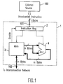
- FIG. 1 illustrates a generic structure of a processing element (PE) 1 in a SIMD computer. All the details which differentiate the processing element of one SIMD computer from another have been omitted, but the essential characteristics of all SIMD computers are shown.
- PE processing element
- the instructions executed by the processing element (PE) 1 are received from an external source 100 shown in Figure 5, which may include, for example, the central controller or an array controller.
- the array controller is in turn connected to a host computer which can be a mainframe or a personal computer.
- the width of the instruction words can be selectively chosen by the designer as required. For example, the instructions could be 32 bits to 256 bits wide.
- each instruction Upon receipt into an instruction register 2, each instruction is executed to access data from the private data memory 3 of the PE 1, and to perform the desired operations on this data using the arithmetic logic unit (ALU) 4, before storing the data back to the private memory 2.
- ALU arithmetic logic unit
- Part of the instruction also controls the transfer of data between the memory 2 and the interconnection network 102 shown in Figure 5.
- the data memory 3 can be hierarchical, comprising registers, cache memory, main memory, etc., in which case the movement of data between various levels of the memory hierarchy is also controlled by the instruction received from the central controller.
- Figure 1 illustrates control signals directly from the instruction register 2 to the private data memory 3 and the ALU 4
- additional control logic can be associated with the instruction register 2 to further decode the instructions received from the central controller before they are applied to the ALU 4 and data memory 3.
- the PEs in almost all SIMD computers can partially or totally disable the current instruction in the instruction register 2 as shown by the dotted line labelled "Disable" in Figure 1.
- This disabling capability is extremely useful for performing different operations on different data, but is inflexible and therefore very inefficient, in most situations identified above, for executing dissimilar sequences of instructions on different PEs.
- Another object of the present invention is to provide a SIMD computer having processing elements in which the processing element can execute dissimilar sequences of instructions.
- the inventive structure takes advantage of the feature of SIMD machines having simple and efficient hardware which can be used optimally by scheduling the calculations and communication at compile time.
- the degradation of efficiency can be eliminated effectively and the applicability of SIMD machines can be extended to a much larger set of applications.
- the present invention includes three hardware configurations, as discussed below, and a method of integrating them in the processing elements (PEs) of an SIMD parallel computer to provide these PEs the capability of executing dissimilar sequences of instructions.
- PEs processing elements
- a single instruction multiple data stream (SIMD) array processor which includes a plurality of processing elements (PEs), each for receiving an instruction broadcasted from an external source.
- Each of the plurality of processing elements include a memory for storing data therein, a first multiplexer for receiving the broadcasted instruction, an instruction register, coupled to the memory and to the first multiplexer, for receiving an output from the first multiplexer and for providing control signals and an output to the memory, a storage means coupled to the instruction register and to the memory, for storing at least one instruction, the at least one instruction including data read out of the memory and placed in the storage means, the first multiplexer further receiving the at least one instruction in the storage means; and means for modifying the at least one instruction to respectively create a modified instruction and storing the modified instruction in the storage means to be executed as a next instruction, the modified instruction being used repeatedly when selected by the broadcasted instruction from the external source.
- the modifying means includes a device for selecting one of the broadcaste
- the invnetive SIMD computer has processing elements in which the processing element can execute dissimilar sequences of instructions and in which the restriction of executing identical instructions in all PEs which often degrades the efficiency significantly in the conventional systems, is overcome by using the local instruction buffer or the local instruction memory. Processing efficiency can be maintained and the applicability of SIMD machines can be extended to a much larger set of applications.
- PEs processing elements
- Figure 2 there is shown a structure for enabling the processing elements (PEs) of a SIMD computer to execute dissimilar sequences of instructions.
- the number of PEs which are typically in an array and are interconnected as is known in the art and as shown in Figure 5, can be selected according to the requirements and applications of the user. Typical numbers vary from 8 to 65536.
- Figures 2-4 illustrate a single processing element. Further, only the principal connections which are required for an understanding of the present invention are shown. The lines may be uni- or bi-directional as required and as illustrated.
- the external source 100 in Figure 5 issues broadcast instructions in parallel to the PEs via an instruction bus 101 as shown in Figure 5.
- a processing element (PE) 20 includes an instruction register 21, a private data memory 22, and an ALU 23, similarly to the conventional system shown in Figure 1.
- the PE 20 also includes a Local Instruction Buffer 24 in which an instruction can be assembled using data from the PE's private data memory 22 and then this locally assembled instruction can be executed by the PE 20.
- the PE 20 also includes a multiplexer 25, and select bits 26.
- a special instruction ILOAD (x, A) (e.g., "instruction load") is added to the instruction set of the PE 20 which causes the m-byte to be read out of the location A of the data memory 22 and to be placed in bytes m x x through m x (x + 1)-1 of the local instruction buffer 24, where x and A are immediate operands of the ILOAD instruction.
- the PE 20 sends the address "A" of the m bytes in memory 22, along with a read signal, to the memory on control lines 29. It also sends the index x and a write enable signal to the local instruction buffer 24 on control lines 28.
- the read signal on control line 29 causes the m bytes at location A in the memory to be retrieved and placed on bus 27 which connects to the local instruction buffer 24 in addition to the ALU 23.
- the write enable signal on control line 28 causes the m bytes on bus 27 to be written into local instruction buffer bytes m, x through m (x + 1) - 1.
- the PEs 20 are assumed to have the ability to locally modify the address field A of the ILOAD instruction by adding a local offset to it.
- the offset can be a default base register, or a contents of a general purpose register. Modifying the address filed of a broadcast instruction in this manner is well known in the art.
- the multiplexer 25 which receives an instruction input of i-bytes from the external source 100 (e.g., an array controller or central controller) as shown in Figure 5 and an input of i bytes from the local instruction buffer 24, selects each m-byte block of the instruction from either the central controller or the instruction in the local instruction buffer 24 of the PE, in each machine cycle.
- the machine cycle is the basic timing cycle of the external source (e.g., the central controller or array controller).
- the selected instruction is placed in the instruction register (buffer) 21 to be executed as the next instruction.
- the selection by the multiplexer 25 is controlled by the SELECT_BITS issued by select bits generator 26, each bit controlling the multiplexer 25 for m-bytes of the instruction word.
- the select bits 26 are set by the central controller using another new instruction, SET_SEL_BITS, and the value to be placed in the select bits 26 is provided as an immediate operand of this instruction.
- the SET_SEL_BITS instruction is also broadcast by the external source to all PEs. Lines 26a carry the immediate operand of the SET_SEL_BITS instruction from instruction register 21 to the select bits 26 to set the select bits 26.
- the select bits generator 26 are automatically cleared in each machine cycle unless they are being set explicitly by the SET_SEL_BITS instruction.
- the select bits generator 26 allows for partial modification of the instruction broadcasted from the central controller, based on processor specific data by allowing some microoperations in the instruction to come from the central controller and other microoperations to be taken from the processor's local instruction buffer 24.
- select bits generator 26 Another, more effective, way of using the select bits generator 26 is to allow each select bit to control one microoperation rather than a block of m-bytes.
- an instruction word is much longer than a data memory word. If the two lengths were comparable, a single select bit could be used to choose between the local instruction in the local instruction buffer 24 and the broadcasted instruction from the central controller. Typically, an instruction word is 16 to 256 bits long whereas a data memory word is 32 or 64 bits long.
- the microoperations that control the select bits generator 26 and the local instruction buffers 24 should preferably be received only from the broadcasted instruction. This feature can be enforced in hardware by wiring the corresponding lines of the broadcasted instruction directly to the instruction register 21.
- the microoperations (or m-byte blocks), which are not identical in the instructions to be executed by all PEs, are assembled in the local instruction buffer 24.
- the m-byte blocks needed to modify the instruction in each P are calculated in each PE's private data memory 22. This step, explained in detail below, can be omitted under certain conditions which are also explained below.
- an appropriate number of ILOAD instructions one for each m-byte block to be loaded into the local instruction buffer 24, are issued by array controller 100 to move the m-byte blocks from each PE's private data memory 22 to the local instruction buffer 24.
- a SET_SEL_BITS instruction is also issued by the central controller. Execution of this instruction causes the next instruction to include processor-specific microoperations from the local instruction buffer 24 while the remaining microoperations are taken from the instruction broadcast by The central controller.
- a sequence of instruction hereafter called the build_code_sequence is broadcast from the array controller 100 (external source) to each PE.
- the above-mentioned m-byte words calculated by the build_code_sequence can be different in each PE.
- the ability of each PE to locally disable the execution of any broadcast instruction as discussed earlier and as shown in Figure 2 can also be used to assemble different m-byte words in each PE.
- the execution of a broadcast instruction is disabled locally in a PE based on processor specific data such as a particular bit in a condition code register, which can be set by other instructions of the PE's instruction set.
- Figure 6 shows the data memory 22 of two PEs of the representative SIMD computer, after the execution of build_code_sequence instructions.
- the m-byte blocks of an instruction word calculated by these instructions, and stored in the PEs' private data memory 22 starting at address A, are different in the two PEs and labelled as code 1 and code 2.
- the build_code_sequence instruction may not be needed if the m-byte words needed to modify a broadcast instruction have already been computed to modify a previously broadcast instruction, and saved in identical locations in the PE's local data memory 22 for later use.
- the different sets of m-byte words used by different PEs to modify a broadcast instruction can be calculated at compile time, and all such sets of m-byte words can be loaded in all PEs private data memory 22, when the program is loaded in the array controller 100.
- Figure 7 shows two PEs. PE1 and PE2, each storing two sets of m-byte blocks, labeled code 1 and code 2. It is assumed that code blocks are of the same length, (e.g., l m-byte words), and that each code block is stored in an identical location in each PE, starting at address B1 and B2, respectively.
- code blocks are of the same length, (e.g., l m-byte words), and that each code block is stored in an identical location in each PE, starting at address B1 and B2, respectively.
- l ILOAD instructions are broadcast from the central controller.
- the addresses A, A +1, ..., A + l-1, specified in the broadcast ILOAD instruction are modified by PE 1 to addresses B1, B1 + 1, ..., B1 + l-1, and by PE 2 to B2, B2 + 1, ..., B2 + l-1, respectively, by adding processor specific local offset as explained above.
- PE1 will have code 1 loaded into its local instruction buffer 24 while PE2 will have code 2 loaded into its local instruction buffer.
- the PEs can partially or totally disable the current instruction in the instruction register 2 as shown by the dotted line labelled "Disable” in Figure 2.
- the PEs For every instruction in a sequence of dissimilar instructions, the PEs have to execute several ILOAD instructions and one SET_SEL_BITS instruction. If the dissimilar instruction sequences are executed repeatedly, the cost of build_load_sequence instructions can be amortized over the repeated executions of the dissimilar instruction sequences.
- Figure 3 illustrates a second aspect according to the present invention and illustrates an improvement to the structure (and related method) shown in Figure 2.
- the local instruction buffer of Figure 2 is replaced by the program memory 34 shown in Figure 3.
- the program memory includes a large number (preferably 1K to 16K words) of instruction words.
- Processor specific instructions can be assembled in the instruction words of the program memory by using the ILOAD instruction as defined earlier.
- the ILOAD instructions have an additional immediate operand to select an instruction word in the program memory.
- the improved processing element (PE) 30 of Figure 3 includes an instruction register 31, a private data memory 32, and an ALU 33, similarly to the conventional system shown in Figure 1 and the structure 20 according to the first aspect of the invention shown in Figure 2.
- PE 30 also includes a program memory 34, an Icount register 35, a base register 36, a multiplexer 37, zero detector 38, an adder 39, and a multiplexer 40.
- the improved PE 30 is described hereinbelow.
- the local instruction buffer 21 shown in Figure 2 is replaced by a program memory 34, as shown in Figure 3, including a large number of instruction words.
- the ILOAD instruction now has three operands and is specified mnemonically as ILOAD(x, A, B).
- the x and A operands have same function and meaning as described above.
- the new operand B selects the instruction word in the program memory 34 that will be updated by the ILOAD instruction.
- m-byte word is read from the PE's data memory at address A, and stored in bytes m, x to m (x + 1) -1 in the PE's program memory at address B.
- Each instruction word in the program memory can require a different pattern of select bits.
- the support for the select bits is not shown and therefore all m-byte blocks of an instruction are taken from the broadcast instruction, or all of them are taken from the processor's local program memory 34.
- the select bits can be separated and combined with the output of zero detection logic 38 to generate control signals for the multiplexer 37.
- the Icount register 35 and the base register 36 are provided to execute a sequence of instructions from the PE's private instruction memory 34. Registers 35, 36 replace the Sel_Bits register 26 of Figure 2.
- a first instruction, SET_ICOUNT (x), is for writing an immediate operand into the Icount register 35. Exectuing SET_ICOUNT (x) causes the Icount register 35 to be set to x.
- a second instruction LOAD_BASE (A) is for reading data (m-bytes) from location A of data memory 32 and storing the data being read out of the data memory 32 into the base register 36. The Icount register 35 always counts down to zero, unless it is being set by the current instruction.
- a nonzero value in the Icount register 35 causes the PEs to choose (via multiplexer 37) the next instruction from their own program memory 34, rather than the broadcasted instruction from the central controller.
- the instruction address for the program memory 34 is obtained by subtracting the contents of the Icount register 35 from the base register 36.
- the address of the last instruction in the sequence is placed in the Base register 36 using the LOAD_BASE instruction. After executing a broadcasted LOAD_BASE instruction, each PE can have a different value in its register 36.
- the value s is placed in the Icount register 35, which causes the next S instructions to be executed out of the processor's local program memory 34.
- the multiplexer 37 that chooses between the local and broadcasted instruction can be controlled directly by an extra bit in the broadcasted instruction, rather than by the zero detector 38 attached to the Icount register35.
- A denotes the address lines for program memory 34.
- WE are the i ⁇ m write enable signals, one for each m-byte block of an instruction word.
- the WE signals are normally high, but one of them is set low in an ILOAD instruction, and enables the data read out of the data memory 32 to be written into the corresponding m-byte block of the word in program memory 34 selected by the address lines A.
- the lines labeled DIN bring the data read from the data memory by the ILOAD instruction to the program memory 34.
- the output of multiplexor 40 provides the address lines A for the program memory.
- the address presented to the program memory is an immediate operand of the broadcast ILOAD instruction, and carried on line 40a from the instruction register 31 to the multiplexor 40.
- the logical "AND" of all WE signals is used as the control input for multiplexor 40. Because one of the WE signals is low during an ILOAD instruction, the control input to multiplexor 40 is low during an ILOAD instruction, and therefore, the address on line 40a is selected as the address presented to the program memory 34.
- the multiplexor selects its other input provided by the subtraction circuitry 39, and the address presented to the program memory is the result of subtracting ICOUNT register 35 from the Base register 36.
- the entire instruction sequences are assembled in the program memory 34 before any instruction from the sequence is executed. This operation can be accomplished by assembling one instruction at a time in consecutive locations of the program memory.
- the method of assembling an instruction in a specified word B of the program memory 34 is the same as that described earlier for assembling an instruction in local instruction buffer 24.
- the PE's program memory 34 can be executed by the PEs as follows. Assuming that there are S instructions in the sequence, the first instruction is assumed to be stored at address A and the last instruction therefore is stored at address A+ S-1. First, the LOAD-BASE (A+S) instruction is issued to load the value A+S in the base register 36. Next, the SET-ICOUNT (S) instruction is issued to load the value S in the ICOUNT register 35.
- A+S LOAD-BASE
- S SET-ICOUNT
- the ICOUNT register will countdown from S to O, and while this register is non-zero for S cycles taking values S, S-1, S3, ..., 1, instructions will be read from program memory from locations A, A+1, ..., A+S-1, and these will be selected by the multiplexor 37 to be placed in instruction register 31 for execution.
- the LOAD-BASE and SET.ICOUNT instructions are broadcast from the central controller 100 to all PEs.
- the PEs may add a processor specific offset to the argument of LOAD-BASE instruction before storing it in the base register 36.
- the compiler can generate these instruction sequences to be loaded into the PE's local program memory 34, when the program is loaded in the array controller 100.
- all instruction sequences can be loaded in each PE's local program memory 34, and the PEs can locally modify the operand of the LOAD_BASE instruction to select the desired sequence.
- the instruction stored in the local program memory 34 is not allowed to change the ICOUNT register.
- LOAD_BASE and ILOAD opcodes should also not be issued from local program memory 34.
- Figure 4 illustrates a third aspect according to the present invention and yet another variation of the above-described scheme.
- the improved processing element 41 of Figure 4 includes an instruction register 42, a private data memory 43, and an ALU 44, similarly to the conventional system shown in Figure 1 and the structure 20, 30 according to the first and second aspects of the invention respectively shown in Figures 2 and 3.
- the improved PE 41 also includes a program memory 45, a microsequencer 46 and a multiplexer 48.
- the address generation logic for the PE's local program memory 34 shown in Figure 3 is replaced by a commercially available microsequencer 46 (e.g., 2910 chips commercially available from Advanced Micro Devices (AMD), IDT, Vittesse, etc.).
- a commercially available microsequencer 46 e.g., 2910 chips commercially available from Advanced Micro Devices (AMD), IDT, Vittesse, etc.
- the microsequencer 46 subsumes the function of the Icount register 35 and the Base register 36 (shown in Figure 3), the adder 39 and multiplexer 40 used for generating address for the PE's program memory 34, and the zero detector 38 used with the Icount register 35 shown in Figure 3.
- the WE, DIN, and A signals are used in the same manner as in the apparatus of Figure 3 and are described above.
- the apparatus of Figure 4 is the same as that of Figure 3 except that microsequencer 46 is used to implement the function of Base and Icount registers, subtraction circuit 39 and zero detector 38.
- the operation of this apparatus is the same as that of the apparatus of Figure 3. Thus, for clarity and brevity, such is not described herein.
- a performance advantage results because of the private instruction memory (e.g., the local instruction buffer 24 in Figure 2 and the program memory 34/45 in Figures 3-4) in each PE, in the following frequently occurring situations.
- the spatial decomposition of data in a straight-forward manner may require different types of calculations to be performed on different data segments.
- the boundary points and interior points may require different processing.
- the different instruction sequences needed to process the data in different processors can be stored at the same address in the private instruction memories of the PEs, and can be applied to the private data of PEs by broadcasting the identical base address of these instructions and the instruction counts from the central controller 100.
- the choice of the instruction sequence to be applied to the data segment in a PE may depend on the value of the same or different variables in the PEs, rather than on the spatial position of the data in the global structure.
- one row of the matrix is the pivot row and must be processed differently from the other rows.
- a new row becomes the pivot row in each step. If the matrix is partitioned among the processors by rows, then in any given step the processors containing the pivot row must execute a different sequence of instructions than the processors containing non-pivot rows.
- each PE in the program memory.
- Each PE selects which sequence it executes by storing the corresponding base address in the base address register 36 shown in Figure 3.
- a method and apparatus are provided in which a local instruction buffer or a local instruction memory is utilized, thereby allowing the applicability of SIMD machines to be extended to a much larger set of applications and in which the need to execute different instructions in all PEs simultaneously does not degrade the efficiency of the SIMD machines.
- a SIMD computer includes a plurality of processing elements, each of which has a local instruction source and a multiplexer for modifying the instruction to execute dissimilar sequences of instructions.
- a local instruction buffer for storing a single instruction, or several blocks of several instructions is employed.
- the results of operations by the ALU are stored in the processors' local data store, and the modified instruction, or a sequence of modified instructions saved in the local instruction store, can be used by the SIMD processors repeatedly, when selected by the global instruction.
- a key advantage of the present invention is that, while in the conventional systems the type of modifications possible locally are limited by the hardware support implemented in the processing elements, in the present invention any imaginable modification is possible because the general purpose ALU computes the modified instruction.
- the present invention includes means for modifying the whole instruction altogether.
- the present invention allows for the capability in the processing elements in a row to locally modify the identical instructions they receive.
- broadcast instructions are modified locally within the processor by substituting them partially or fully with the information contained in the local instruction buffer, which in turn is loaded from the processor's local data memory under the control of the broadcast programs. Since the processors do not autonomously fetch instructions and modify the broadcast instructions instead, under control of the broadcast program, instruction fetch and decode logic and synchronization circuit are not needed in each processing element.
- the present invention allows the broadcast instruction issued by an external source (e.g., central controller, array controller, etc.) to be modified by the array elements (e.g., the processing element) of the SIMD machine.
- an external source e.g., central controller, array controller, etc.
- the array elements e.g., the processing element
- the local instruction buffer 24 in Figure 2 receives the m-byte blocks to be stored in it from an output of data memory 22 on bus 27.
- the data (m-byte blocks or microoperations) to be stored in the local instruction buffer 24 can be taken from the output of ALU 23.
- the microroperations to be stored in the instruction words of program memory 34 and/or the address to be loaded in Base register 36 can be taken from the output of ALU 33 rather than the output of data memory 32.
Landscapes
- Engineering & Computer Science (AREA)
- Theoretical Computer Science (AREA)
- Software Systems (AREA)
- Physics & Mathematics (AREA)
- General Engineering & Computer Science (AREA)
- General Physics & Mathematics (AREA)
- Computer Hardware Design (AREA)
- Computing Systems (AREA)
- Multi Processors (AREA)
- Advance Control (AREA)
Applications Claiming Priority (2)
| Application Number | Priority Date | Filing Date | Title |
|---|---|---|---|
| US378756 | 1995-01-26 | ||
| US08/378,756 US5680597A (en) | 1995-01-26 | 1995-01-26 | System with flexible local control for modifying same instruction partially in different processor of a SIMD computer system to execute dissimilar sequences of instructions |
Publications (2)
| Publication Number | Publication Date |
|---|---|
| EP0724221A2 true EP0724221A2 (de) | 1996-07-31 |
| EP0724221A3 EP0724221A3 (de) | 1997-03-12 |
Family
ID=23494430
Family Applications (1)
| Application Number | Title | Priority Date | Filing Date |
|---|---|---|---|
| EP95112674A Withdrawn EP0724221A3 (de) | 1995-01-26 | 1995-08-11 | Verfahren und Vorrichtung zur Ausführung unähnlicher Befehlsfolgen in einem Prozessor eines Einzelbefehl- und Mehrfahrdatenrechners (SIMD) |
Country Status (3)
| Country | Link |
|---|---|
| US (1) | US5680597A (de) |
| EP (1) | EP0724221A3 (de) |
| JP (1) | JP3101560B2 (de) |
Cited By (10)
| Publication number | Priority date | Publication date | Assignee | Title |
|---|---|---|---|---|
| DE19651075A1 (de) * | 1996-12-09 | 1998-06-10 | Pact Inf Tech Gmbh | Einheit zur Verarbeitung von numerischen und logischen Operationen, zum Einsatz in Prozessoren (CPU's), Mehrrechnersystemen, Datenflußprozessoren (DFP's), digitalen Signal Prozessoren (DSP's) oder dergleichen |
| FR2757973A1 (fr) * | 1996-12-27 | 1998-07-03 | Sgs Thomson Microelectronics | Processeur de traitement matriciel |
| DE19654846A1 (de) * | 1996-12-27 | 1998-07-09 | Pact Inf Tech Gmbh | Verfahren zum selbständigen dynamischen Umladen von Datenflußprozessoren (DFPs) sowie Bausteinen mit zwei- oder mehrdimensionalen programmierbaren Zellstrukturen (FPGAs, DPGAs, o. dgl.) |
| WO2007014404A1 (de) * | 2005-08-04 | 2007-02-08 | On Demand Microelectronics Ag | Digitale rechnereinrichtung mit parallelverarbeitung |
| US7904695B2 (en) | 2006-02-16 | 2011-03-08 | Vns Portfolio Llc | Asynchronous power saving computer |
| US7904615B2 (en) | 2006-02-16 | 2011-03-08 | Vns Portfolio Llc | Asynchronous computer communication |
| US7913069B2 (en) | 2006-02-16 | 2011-03-22 | Vns Portfolio Llc | Processor and method for executing a program loop within an instruction word |
| US7937557B2 (en) | 2004-03-16 | 2011-05-03 | Vns Portfolio Llc | System and method for intercommunication between computers in an array |
| US7966481B2 (en) | 2006-02-16 | 2011-06-21 | Vns Portfolio Llc | Computer system and method for executing port communications without interrupting the receiving computer |
| US9424045B2 (en) | 2013-01-29 | 2016-08-23 | Arm Limited | Data processing apparatus and method for controlling use of an issue queue to represent an instruction suitable for execution by a wide operand execution unit |
Families Citing this family (44)
| Publication number | Priority date | Publication date | Assignee | Title |
|---|---|---|---|---|
| US6317819B1 (en) | 1996-01-11 | 2001-11-13 | Steven G. Morton | Digital signal processor containing scalar processor and a plurality of vector processors operating from a single instruction |
| US5822606A (en) * | 1996-01-11 | 1998-10-13 | Morton; Steven G. | DSP having a plurality of like processors controlled in parallel by an instruction word, and a control processor also controlled by the instruction word |
| US6088783A (en) * | 1996-02-16 | 2000-07-11 | Morton; Steven G | DPS having a plurality of like processors controlled in parallel by an instruction word, and a control processor also controlled by the instruction word |
| US5854905A (en) * | 1996-09-03 | 1998-12-29 | Intel Corporation | Extensible bios for boot support of devices on multiple hierarchical buses |
| EP0858168A1 (de) | 1997-01-29 | 1998-08-12 | Hewlett-Packard Company | Feldprogrammierbarer Gatterprozessor |
| EP1029266B1 (de) * | 1997-11-07 | 2007-05-16 | Altera Corporation | VERFAHREN UND GERÄT FÜR EFFIZIENTE, SYNCHRONE MIMD-OPERATIONEN MIT iVLIW PE-ZU-PE KOMMUNIKATIONEN |
| US6567834B1 (en) | 1997-12-17 | 2003-05-20 | Elixent Limited | Implementation of multipliers in programmable arrays |
| DE69827589T2 (de) | 1997-12-17 | 2005-11-03 | Elixent Ltd. | Konfigurierbare Verarbeitungsanordnung und Verfahren zur Benutzung dieser Anordnung, um eine Zentraleinheit aufzubauen |
| DE69841256D1 (de) | 1997-12-17 | 2009-12-10 | Panasonic Corp | Befehlsmaskierung um Befehlsströme einem Prozessor zuzuleiten |
| US6862732B1 (en) | 1998-02-25 | 2005-03-01 | Metaserver, Inc. | Method and apparatus for event-driven processing of data |
| US6052769A (en) * | 1998-03-31 | 2000-04-18 | Intel Corporation | Method and apparatus for moving select non-contiguous bytes of packed data in a single instruction |
| US6728862B1 (en) * | 2000-05-22 | 2004-04-27 | Gazelle Technology Corporation | Processor array and parallel data processing methods |
| US7127593B2 (en) * | 2001-06-11 | 2006-10-24 | Broadcom Corporation | Conditional execution with multiple destination stores |
| US20070169022A1 (en) * | 2003-06-18 | 2007-07-19 | Jones Anthony M | Processor having multiple instruction sources and execution modes |
| US7594069B2 (en) * | 2004-02-26 | 2009-09-22 | Ati Technologies, Inc. | Method and apparatus for single instruction multiple data caching |
| JP4477959B2 (ja) * | 2004-07-26 | 2010-06-09 | 独立行政法人理化学研究所 | ブロードキャスト型並列処理のための演算処理装置 |
| US20060168090A1 (en) * | 2005-01-07 | 2006-07-27 | United Technologies Corporation | Remote integrated subsystems in an aircraft or the like |
| US7725691B2 (en) * | 2005-01-28 | 2010-05-25 | Analog Devices, Inc. | Method and apparatus for accelerating processing of a non-sequential instruction stream on a processor with multiple compute units |
| US7516301B1 (en) * | 2005-12-16 | 2009-04-07 | Nvidia Corporation | Multiprocessor computing systems with heterogeneous processors |
| DE602007011841D1 (de) * | 2006-02-16 | 2011-02-24 | Vns Portfolio Llc | Ausführung von Anweisungen direkt von der Eingabequelle aus |
| EP2057554A1 (de) * | 2006-08-20 | 2009-05-13 | Ambric Inc. | Prozessor mit mehreren anweisungsquellen und ausführungsbetriebsarten |
| KR100990526B1 (ko) * | 2006-08-23 | 2010-10-29 | 닛본 덴끼 가부시끼가이샤 | 혼합 모드 병렬 프로세서 시스템 및 방법과 혼합 모드 병렬 프로세서 프로그램이 기록되어 있는 컴퓨터 판독가능 기록매체 |
| US7441099B2 (en) * | 2006-10-03 | 2008-10-21 | Hong Kong Applied Science and Technology Research Institute Company Limited | Configurable SIMD processor instruction specifying index to LUT storing information for different operation and memory location for each processing unit |
| US7961872B2 (en) * | 2006-12-04 | 2011-06-14 | Lsi Corporation | Flexible hardware architecture for ECC/HECC based cryptography |
| GB0907559D0 (en) * | 2009-05-01 | 2009-06-10 | Optos Plc | Improvements relating to processing unit instruction sets |
| JP5708634B2 (ja) * | 2010-02-24 | 2015-04-30 | 日本電気株式会社 | Simdプロセッサ |
| US20110314256A1 (en) * | 2010-06-18 | 2011-12-22 | Microsoft Corporation | Data Parallel Programming Model |
| US8589867B2 (en) | 2010-06-18 | 2013-11-19 | Microsoft Corporation | Compiler-generated invocation stubs for data parallel programming model |
| US9665372B2 (en) * | 2014-05-12 | 2017-05-30 | International Business Machines Corporation | Parallel slice processor with dynamic instruction stream mapping |
| US9672043B2 (en) | 2014-05-12 | 2017-06-06 | International Business Machines Corporation | Processing of multiple instruction streams in a parallel slice processor |
| US9760375B2 (en) | 2014-09-09 | 2017-09-12 | International Business Machines Corporation | Register files for storing data operated on by instructions of multiple widths |
| US9720696B2 (en) | 2014-09-30 | 2017-08-01 | International Business Machines Corporation | Independent mapping of threads |
| US9977678B2 (en) | 2015-01-12 | 2018-05-22 | International Business Machines Corporation | Reconfigurable parallel execution and load-store slice processor |
| US10133581B2 (en) | 2015-01-13 | 2018-11-20 | International Business Machines Corporation | Linkable issue queue parallel execution slice for a processor |
| US10133576B2 (en) | 2015-01-13 | 2018-11-20 | International Business Machines Corporation | Parallel slice processor having a recirculating load-store queue for fast deallocation of issue queue entries |
| US9983875B2 (en) | 2016-03-04 | 2018-05-29 | International Business Machines Corporation | Operation of a multi-slice processor preventing early dependent instruction wakeup |
| US10037211B2 (en) | 2016-03-22 | 2018-07-31 | International Business Machines Corporation | Operation of a multi-slice processor with an expanded merge fetching queue |
| US10346174B2 (en) | 2016-03-24 | 2019-07-09 | International Business Machines Corporation | Operation of a multi-slice processor with dynamic canceling of partial loads |
| US10761854B2 (en) | 2016-04-19 | 2020-09-01 | International Business Machines Corporation | Preventing hazard flushes in an instruction sequencing unit of a multi-slice processor |
| US10037229B2 (en) | 2016-05-11 | 2018-07-31 | International Business Machines Corporation | Operation of a multi-slice processor implementing a load/store unit maintaining rejected instructions |
| US9934033B2 (en) | 2016-06-13 | 2018-04-03 | International Business Machines Corporation | Operation of a multi-slice processor implementing simultaneous two-target loads and stores |
| US10042647B2 (en) | 2016-06-27 | 2018-08-07 | International Business Machines Corporation | Managing a divided load reorder queue |
| US10318419B2 (en) | 2016-08-08 | 2019-06-11 | International Business Machines Corporation | Flush avoidance in a load store unit |
| US11860814B1 (en) * | 2020-11-01 | 2024-01-02 | Konda Technologies Inc. | Scalable distributed computing system with deterministic communication |
Family Cites Families (9)
| Publication number | Priority date | Publication date | Assignee | Title |
|---|---|---|---|---|
| US4783738A (en) * | 1986-03-13 | 1988-11-08 | International Business Machines Corporation | Adaptive instruction processing by array processor having processor identification and data dependent status registers in each processing element |
| GB2211638A (en) * | 1987-10-27 | 1989-07-05 | Ibm | Simd array processor |
| US5179714A (en) * | 1988-10-07 | 1993-01-12 | Martin Marietta Corporation | Parallel bit serial data processor |
| US5253308A (en) * | 1989-06-21 | 1993-10-12 | Amber Engineering, Inc. | Massively parallel digital image data processor using pixel-mapped input/output and relative indexed addressing |
| US5212777A (en) * | 1989-11-17 | 1993-05-18 | Texas Instruments Incorporated | Multi-processor reconfigurable in single instruction multiple data (SIMD) and multiple instruction multiple data (MIMD) modes and method of operation |
| US5239654A (en) * | 1989-11-17 | 1993-08-24 | Texas Instruments Incorporated | Dual mode SIMD/MIMD processor providing reuse of MIMD instruction memories as data memories when operating in SIMD mode |
| US5522080A (en) * | 1991-10-24 | 1996-05-28 | Intel Corporation | Centralized control SIMD processor having different priority levels set for each data transfer request type and successively repeating the servicing of data transfer request in a predetermined order |
| US5542074A (en) * | 1992-10-22 | 1996-07-30 | Maspar Computer Corporation | Parallel processor system with highly flexible local control capability, including selective inversion of instruction signal and control of bit shift amount |
| US5511212A (en) * | 1993-06-10 | 1996-04-23 | Rockoff; Todd E. | Multi-clock SIMD computer and instruction-cache-enhancement thereof |
-
1995
- 1995-01-26 US US08/378,756 patent/US5680597A/en not_active Expired - Fee Related
- 1995-08-11 EP EP95112674A patent/EP0724221A3/de not_active Withdrawn
-
1996
- 1996-01-10 JP JP08002639A patent/JP3101560B2/ja not_active Expired - Fee Related
Non-Patent Citations (1)
| Title |
|---|
| None |
Cited By (13)
| Publication number | Priority date | Publication date | Assignee | Title |
|---|---|---|---|---|
| DE19651075A1 (de) * | 1996-12-09 | 1998-06-10 | Pact Inf Tech Gmbh | Einheit zur Verarbeitung von numerischen und logischen Operationen, zum Einsatz in Prozessoren (CPU's), Mehrrechnersystemen, Datenflußprozessoren (DFP's), digitalen Signal Prozessoren (DSP's) oder dergleichen |
| FR2757973A1 (fr) * | 1996-12-27 | 1998-07-03 | Sgs Thomson Microelectronics | Processeur de traitement matriciel |
| DE19654846A1 (de) * | 1996-12-27 | 1998-07-09 | Pact Inf Tech Gmbh | Verfahren zum selbständigen dynamischen Umladen von Datenflußprozessoren (DFPs) sowie Bausteinen mit zwei- oder mehrdimensionalen programmierbaren Zellstrukturen (FPGAs, DPGAs, o. dgl.) |
| US5987488A (en) * | 1996-12-27 | 1999-11-16 | Sgs-Thomson Microelectronics S.A. | Matrix processor |
| US7937557B2 (en) | 2004-03-16 | 2011-05-03 | Vns Portfolio Llc | System and method for intercommunication between computers in an array |
| US7984266B2 (en) | 2004-03-16 | 2011-07-19 | Vns Portfolio Llc | Integrated computer array with independent functional configurations |
| WO2007014404A1 (de) * | 2005-08-04 | 2007-02-08 | On Demand Microelectronics Ag | Digitale rechnereinrichtung mit parallelverarbeitung |
| US7904615B2 (en) | 2006-02-16 | 2011-03-08 | Vns Portfolio Llc | Asynchronous computer communication |
| US7913069B2 (en) | 2006-02-16 | 2011-03-22 | Vns Portfolio Llc | Processor and method for executing a program loop within an instruction word |
| US7966481B2 (en) | 2006-02-16 | 2011-06-21 | Vns Portfolio Llc | Computer system and method for executing port communications without interrupting the receiving computer |
| US7904695B2 (en) | 2006-02-16 | 2011-03-08 | Vns Portfolio Llc | Asynchronous power saving computer |
| US8825924B2 (en) | 2006-02-16 | 2014-09-02 | Array Portfolio Llc | Asynchronous computer communication |
| US9424045B2 (en) | 2013-01-29 | 2016-08-23 | Arm Limited | Data processing apparatus and method for controlling use of an issue queue to represent an instruction suitable for execution by a wide operand execution unit |
Also Published As
| Publication number | Publication date |
|---|---|
| EP0724221A3 (de) | 1997-03-12 |
| US5680597A (en) | 1997-10-21 |
| JPH08241291A (ja) | 1996-09-17 |
| JP3101560B2 (ja) | 2000-10-23 |
Similar Documents
| Publication | Publication Date | Title |
|---|---|---|
| US5680597A (en) | System with flexible local control for modifying same instruction partially in different processor of a SIMD computer system to execute dissimilar sequences of instructions | |
| US5822608A (en) | Associative parallel processing system | |
| US5226131A (en) | Sequencing and fan-out mechanism for causing a set of at least two sequential instructions to be performed in a dataflow processing computer | |
| US6446190B1 (en) | Register file indexing methods and apparatus for providing indirect control of register addressing in a VLIW processor | |
| KR100190738B1 (ko) | 데이타 처리 시스템 및 방법 | |
| US5805915A (en) | SIMIMD array processing system | |
| US4079451A (en) | Word, byte and bit indexed addressing in a data processing system | |
| US5872987A (en) | Massively parallel computer including auxiliary vector processor | |
| EP1038253B1 (de) | Multiverarbeitungsrechner-architektur mit eingeschlossenr mehrheit von speicher-algoritmus-prozessoren in dem speicheruntersystem | |
| KR100638703B1 (ko) | 데이터 프로세싱 시스템용 셀룰러 엔진 | |
| JP2647315B2 (ja) | 動的に複数モードで並列処理するアレイ | |
| US6356994B1 (en) | Methods and apparatus for instruction addressing in indirect VLIW processors | |
| US3943494A (en) | Distributed execution processor | |
| EP0428326A1 (de) | Feldprozessorsystem | |
| CA2006243C (en) | Microcode control apparatus utilizing programmable logic array circuits | |
| US4047247A (en) | Address formation in a microprogrammed data processing system | |
| US20040078554A1 (en) | Digital signal processor with cascaded SIMD organization | |
| CA1321653C (en) | Programmable priority branch circuit | |
| EP0729616B1 (de) | Datenverarbeitungssystem mit datenverarbeitungseinheiten und eine erweiterungsvorrichtung | |
| EP0226103A2 (de) | Adressengenerator für zellularen Feldprozessor | |
| CN100440193C (zh) | 数据处理系统的引擎装置以及相应的数据处理系统和方法 | |
| Robert | Gaussian elimination on distributed memory architectures | |
| Tseng | Systolic array programming |
Legal Events
| Date | Code | Title | Description |
|---|---|---|---|
| PUAI | Public reference made under article 153(3) epc to a published international application that has entered the european phase |
Free format text: ORIGINAL CODE: 0009012 |
|
| AK | Designated contracting states |
Kind code of ref document: A2 Designated state(s): DE FR GB |
|
| PUAL | Search report despatched |
Free format text: ORIGINAL CODE: 0009013 |
|
| AK | Designated contracting states |
Kind code of ref document: A3 Designated state(s): DE FR GB |
|
| STAA | Information on the status of an ep patent application or granted ep patent |
Free format text: STATUS: THE APPLICATION IS DEEMED TO BE WITHDRAWN |
|
| 18D | Application deemed to be withdrawn |
Effective date: 19970913 |