EP0721177A2 - Apparatus for generating an image from a light source and a display medium for displaying an image - Google Patents
Apparatus for generating an image from a light source and a display medium for displaying an image Download PDFInfo
- Publication number
- EP0721177A2 EP0721177A2 EP96300062A EP96300062A EP0721177A2 EP 0721177 A2 EP0721177 A2 EP 0721177A2 EP 96300062 A EP96300062 A EP 96300062A EP 96300062 A EP96300062 A EP 96300062A EP 0721177 A2 EP0721177 A2 EP 0721177A2
- Authority
- EP
- European Patent Office
- Prior art keywords
- image
- hemisphere
- balls
- substrate
- light
- Prior art date
- Legal status (The legal status is an assumption and is not a legal conclusion. Google has not performed a legal analysis and makes no representation as to the accuracy of the status listed.)
- Granted
Links
Images


Classifications
-
- G—PHYSICS
- G09—EDUCATION; CRYPTOGRAPHY; DISPLAY; ADVERTISING; SEALS
- G09F—DISPLAYING; ADVERTISING; SIGNS; LABELS OR NAME-PLATES; SEALS
- G09F9/00—Indicating arrangements for variable information in which the information is built-up on a support by selection or combination of individual elements
- G09F9/30—Indicating arrangements for variable information in which the information is built-up on a support by selection or combination of individual elements in which the desired character or characters are formed by combining individual elements
- G09F9/37—Indicating arrangements for variable information in which the information is built-up on a support by selection or combination of individual elements in which the desired character or characters are formed by combining individual elements being movable elements
- G09F9/372—Indicating arrangements for variable information in which the information is built-up on a support by selection or combination of individual elements in which the desired character or characters are formed by combining individual elements being movable elements the positions of the elements being controlled by the application of an electric field
-
- G—PHYSICS
- G02—OPTICS
- G02B—OPTICAL ELEMENTS, SYSTEMS OR APPARATUS
- G02B26/00—Optical devices or arrangements for the control of light using movable or deformable optical elements
- G02B26/02—Optical devices or arrangements for the control of light using movable or deformable optical elements for controlling the intensity of light
- G02B26/026—Optical devices or arrangements for the control of light using movable or deformable optical elements for controlling the intensity of light based on the rotation of particles under the influence of an external field, e.g. gyricons, twisting ball displays
Definitions
- the entire ball or just the photosensitive hemisphere of the ball may be made from a material, such as PVK (poly-n-vinyl-carbazole) that easily transports photogenerated carriers. It may be sensitized for the actinic radiation by the addition of certain dyes (such as tri-n-nitrol-fluorenone) to make it photoconducting or it may be overcoated by a photogenerating layer, such as selenium that will produce photogenerated carriers that are injected into and conducted by the carrier transporting material.
- PVK poly-n-vinyl-carbazole
- a photogenerating layer such as selenium that will produce photogenerated carriers that are injected into and conducted by the carrier transporting material.
- the ball or the photosensitive hemisphere may also be made from an insulative material such as epoxy or polyethylene pigmented by photoconductive materials such as cadmium sulfide.
- the bichromal balls will be aligned by the uniform external field and while this voltage continues to be applied the actinic radiation exposure will take place. If the (typically) selenium coated hemisphere is also the initially positively charged hemisphere the same behavior as described above will obtain. If, however, this is the initially negatively charged hemisphere, the photoinjection of negative charges into the the plasticizing liquid will cause the charge on this hemisphere to decrease and eventually become positive. Hence the bichromal balls might rotate after a given exposure without a reversal in the field; simply after sufficient exposure.
Abstract
Description
- The present invention relates to an apparatus for generating an image from a light source and to a medium for displaying an image.
- US-A-4,126,854 and 4,143,103 describe a display system in which the display panel is comprised of spherical particles, balls, which have an optical and electric anisotropy due to each hemisphere surface having a different color and electrical charge. These particles are imbedded in a solid substrate and a slight space between each ball and the substrate is filled with a fluid so that the balls are free to rotate, in a changing electrical field, but can not migrate from one location to another. If one hemisphere is black and the other white, each pixel can be turned on or off by the electrical field applied to that location. Each pixel can be individually addressed by applying an electrical field that is greater than the threshold field required for ball rotation, and a full page image can thus be generated.
- This medium is fabricated by first mixing a large number of balls into a solid substrate, curing the substrate, and then soaking the resultant substrate in a plasticizer. The substrate will swell, creating a space around each ball, and the space will fill with the liquid plasticizer, thus allowing each ball to rotate under the effect of an applied electrical field. The result is reusable "electric paper" which can be used, for example, in a raster output scanner, to produce an image from a bit map of electrical fields, or can be used as the flat panel display of a terminal or notebook computer.
- It would be be useful if this substrate could be modified to produce images from exposure to electromagnetic radiation images, either visible light or x-rays. One way of accomplishing this would be to create a sandwich structure in which this substrate is placed adjacent to a photoconductor layer, with radiation transparent electrodes at the distal surfaces. Upon complete exposure of an area of the photoconductor layer the fraction of the voltage that was across that layer would be collapsed onto the adjacent area of the twisting ball substrate, so that the entire voltage across the sandwich structure would now be across this area of substrate. If this voltage now exceeds the threshold voltage the bichromal balls in that area will rotate.
- The problem is that typical threshold switching behavior requires that the photoconductor layer and the substrate have about the same capacitance, which is proportional to the dielectric constant of the layer divided by the actual thickness of the layer. The substrate material has a dielectric constant of about 2.75 and a photoconductor like selenium has a dielectric constant of about 6. This means that if we use a selenium photoconductor to address our twisting ball substrate it must be about twice as thick as the twisting ball substrate. For a twisting ball substrate using 100 micron diameter balls we will have a minimun thickness of about 150 microns. A 300 micron thick photoconductor suitable for addressing the twisting ball display is very thick and expensive and generally not desireable.
- It would be useful, then, to photosensitize the twisting ball display in a more desireable manner. In doing this in the manner of this invention we will find other desireable properties that have further value.
- This invention allows the sheet medium to display a light image by using a first uniform electrical field to reset all of the balls to one state, and then applying a light image , sometimes in the presence of a second electrical field, to produce the recorded image. One hemisphere in this case must have an electrical property that can be modified by light, so that a radiated ball will behave differently than one receiving no light. For example, if material properties are such that an irradiated ball has a reduced dipole moment relative to a non-irradiated ball, and if the second electrical field is not strong enough to rotate an irradiated ball yet strong enough to rotate a non-irradiated ball, an image can be produced. Conversely, if an irradiated ball has a stronger dipole moment that an non-irradiated ball, a similar process will rotate the irradiated balls. Furthermore, if the dipole moment of an irradiated ball is of the opposite sign from that of the non-irradiated balls, the need for a threshold mechanism is eliminated as a field of uniform magnitude and constant direction will suffice to form an image. In this last case several distinct advantages accrue. The operator can watch the recorded image develop with continued exposure and stop the exposure when the desired image density is obtained. The electrical field across the structure, and thus across the photosensitive balls, can be made sufficiently large that high photosensitivity can be obtained.
- A characteristic of the resultant display is that it is a stable image that requires no additional power for as long as it does not change, as compared to a typical LCD (liquid crystal display) that must be refreshed up to 30 times per second. Thus, a notebook computer equipped with this display would required a fraction of the battery power, which is the main component of the weight of a notebook computer.
- An example of the imaging process would be for the system, under the influence of the first electrical field, to align all of the balls in the same polarity, so their photosensitive hemispheres could receive image radiation. After this exposure a second uniform electrical field would be applied , and under the influence of this field the balls that underwent sufficient changes in their electrical properties would overcome the stiction forces that normally bind them to their cavity walls and would rotate. Balls that received less than the threshold exposure would remain in their previous orientations. Hence, exposed balls would present their white hemispheres to a viewer while the unexposed balls would remain black. It should be noted that the reverse side of the display would present the negative to this image.
- The present invention will be described further, by way of examples, with reference to the accompanying drawings, in which:-
- Fig 1 is a simplified view of the locations of the light source, lens, electric field and electric paper;
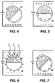
- Fig 2 is a diagram of the charges on a ball having a photoconducting black hemisphere in the initial electric field;
- Fig 3 is a diagram of the charges on a ball having a conducting white hemisphere after radiation;
- Fig 4 is a diagram of the charges on a ball having a conducting white hemisphere after radiation and field reversal;
- Fig 5 is a diagram of the charges on a ball having an insulating white hemisphere in the initial electric field;
- Fig 6 is a diagram of the charges on a ball having an insulating white hemisphere after radiation;
- Fig 7 is a diagram of the charges on a ball having an insulating white hemisphere after radiation and field reversal;
- Fig 8 is an embodiment which uses a stylus to write an image in the form of a line on the medium; and
- Fig 9 is an embodiment which uses a stylus to write an image in the form of a series of linear elements on the medium.
- The use of photosensitive bichromal balls to do optical, or other actinic radiation, image recording is illustrated in Figure 1. A source of light is generated by
element 10 and is focussed on theElectric paper sheet 11 by alens 12. In the case of X-radiation the lens would not be necessary. The sheet of Electric paper consists of a number ofballs 13, one of which is shown as a magnified ball 17. Typically one hemisphere will be made of a white insulative material, such as titanium dioxide dispersed in polyethylene. The other hemisphere will be photosensitive, and of a contrasting color. There are many types of photosensitivity that can be incorporated in the behavior of this hemisphere, but for the purposes of illustration we will limit these to the two major classes of photoconductive and photoinjective behavior. - Because the two hemispheres of the balls are made from different materials, they will develop different double layer characteristics in contact with the dielectric plasticizing liquid (for a good discussion of the double layer reference is made to "Microprocessing and Technology, Asaji Kondo, 1979). Thus in the presense of an electrical field they will develop different values of surface charge density. This behavior has been described in US-A-4,126,854, No. 4,143,103 and 5,262,098, and is the basis of the dipole behavior exhibited by such bichromal balls.
- If one hemisphere of the bichromal ball responds electrically to light exposure the corresponding change in surface charge density will superimpose on the dark surface charge condition, resulting in a change in the electrical behavior of the bichromal ball upon exposure to actinic radiation. Typically, then, to take advantage of this property, a uniform electrical field is applied at the
surfaces 14 to orient all of the balls in one direction and then actinic radiation is applied and the field reversed to orient either only the exposed balls or only the unexposed balls in the other direction, producing a stored image. (Depending on the photoresponse of the bichromal ball, the ball rotation upon actinic light exposure may take place without the change in field direction.) - If the bichromal ball is to exhibit photoconductive behavior, there are several general types of structure that will obtain this and that are well known in the art. The entire ball or just the photosensitive hemisphere of the ball may be made from a material, such as PVK (poly-n-vinyl-carbazole) that easily transports photogenerated carriers. It may be sensitized for the actinic radiation by the addition of certain dyes (such as tri-n-nitrol-fluorenone) to make it photoconducting or it may be overcoated by a photogenerating layer, such as selenium that will produce photogenerated carriers that are injected into and conducted by the carrier transporting material. The ball or the photosensitive hemisphere may also be made from an insulative material such as epoxy or polyethylene pigmented by photoconductive materials such as cadmium sulfide. These structures share the common behavior that in the presence of an electrical field and upon exposure to actinic radiation hole/electron pairs are photogenerated and one or both of these will move in the electrical filed, changing the charge distribution of the bichromal ball.
- In the case where X-Ray images are to recorded, the potoconductors will typically be made from elements having high atomic number. Thus selenium and lead oxide are widely used photoconductors for this purpose.
- A less well known but very suitable photosensitive process utilizes the photoinjection of carriers from a photoconductor, such as selenium, into a surrounding dielectric liquid. Thus if one hemisphere of a bichromal ball made from insulative material is coated with a thin selenium layer (by evaporation, for example) it will exhibit this behavior. In the presense of an electrical field and upon exposure to actinic light photogenerated carriers will be injected into the plasticizing liquid from the selenium and will be transported away from the surface, leaving it with a net charge.
- Another photosensitive mechanism is derived from the surface photoeffect. Many semiconductor materials exhibit a charge redistribution upon exposure to actinic light as charges trapped near the surface are driven into the bulk of the material. The re-distribution of charge results in a measureable change in the electrostatic potential at the surface. This change is known as the surface photovoltage. This change in surface potential also results in a change in dipole moment. For example, titanium dioxide has been observed to change its surface potential by several volts upon exposure to modest light levels. This material is particularly interesting because it is also a white pigment. Thus one side of a bichromal ball which contains such a pigment will also have an intrinsically photosensitive dipole moment.
- The photoresponsive rotation of the bichromal balls depends upon the structure of the balls. The balls are generally contained within spherical cavities filled with dielectric liquid. Upon the application of an electrical field they will both rotate as a dipole and translate as a monopole. The dipole behavior depends upon the difference in surface charge between the two hemispheres of the balls. The monopole behavior depends upon the sum of the surface charges. Thus, equal positive and negative charges on the hemispheres will create a dipole with resulting rotation in a uniform electrical field, but there will be no monopole and thus no linear motion. Most commonly there is both a dipole and a monopole behavior. The monopole behavior drives the ball into the cavity wall where intimate contact allows van der Wahl and other forces to operate and create an adhesion of the ball to the wall. This creates a threshold behavior. Voltages applied to the bichromal ball below a certain value will not cause rotation whereas voltages above a certain value will. Generally, smaller balls require lower voltages to rotate.
- These forces determine the algorithim of voltages that must be applied to a sheet of photosensitive Electric Paper to record an image. Typically, for a sheet of Electric Paper containing a monolayer of bichromal balls with an average diameter of 80 microns, 50 volts will be applied to both orient the balls in a common direction and to provide the necessary electrical field to photosensitize the balls.
- In the case of photoconductor type of photosensitivity, exposure will take place while this voltage is applied. Positive carriers will move toward the negative addressing electrode, toward which the hemisphere which was initially charged positively was already facing, thus increasing the positive charge at this hemisphere. Likewise, the negative carriers will move toward the side facing the positive addressing electrode. Upon reaching this new distribution, some of the charge carriers will become trapped at their respective surfaces by any of various well-known trapping mechanisms. This trapped charge will persist for some time after the radiation is removed. In this manner, exposure of the bichromal ball to actinic radiation will increase the dipole moment of the ball. If, after radiation is removed, the uniform addressing field is reversed, its magnitude can be decreased to such a value that only the bichromal balls which have been exposed to a certain level of actinic radiation will rotate.
- Grey scale response can be obtained by using bichromal balls with a range of diameters, or balls with a range of photoconductive response. (Smaller bichromal balls will rotate at lower threshold voltages, in general.)
- In the case of the photoinjection type of photosensitivity, a somewhat different type of behavior can obtain. Once again, the bichromal balls will be aligned by the uniform external field and while this voltage continues to be applied the actinic radiation exposure will take place. If the (typically) selenium coated hemisphere is also the initially positively charged hemisphere the same behavior as described above will obtain. If, however, this is the initially negatively charged hemisphere, the photoinjection of negative charges into the the plasticizing liquid will cause the charge on this hemisphere to decrease and eventually become positive. Hence the bichromal balls might rotate after a given exposure without a reversal in the field; simply after sufficient exposure.
- It should be noted that the two hemispheres of the bichromal balls could each have photosensitive properties. If one had ordinary photoconductor properties and the other had the photoinjection type of property described in the latter half of the above paragraph, both sequential exposure to two different images and simultaneous exposure to two images received through the two sides of the display would result in a recorded image that was the pixel by pixel difference of the two input images. This property is useful for such applications as change detection.
- In another embodiment of the invention, a stylus is used to write an image on the display medium. This embodiment is shown in Fig 8. The
stylus 21 contains anelectriode 22 at its tip for applying the electric field to the medium 25. This field is applied only in the region of the stylus, and is thus used to alter the image in that region, and would be used in a manner similar to that of a conventional pen writing on a piece of paper. It is an unavoidable fact that such an electrode will exhibit a fringe field extending around the stylus. Although the field directly below thestylus 26 has a direction which is substantially normal to the plane of the paper, thefringe field 27 necessarily has a direction away from the normal, and is thus undesirable as it will cause improper rotation of balls. However, the ill efects of the fringe field can be avoided by the use of photosensitive balls. By use of asuitable radiation source 23 within the stylus, a spot of light can be projected via suitable optical means 24 onto the medium directly below the electrode, at which point the field has the proper orientation. In this manner, only balls in the presence of a desirable field direction will have their dipole mements enhanced in such a way as to cause rotation. Balls in the fringe areas will not be exposed to radiation and, hence, will not rotate. This method requires a suitable mechanism for photosensitivity by which exposed balls have enhanced dipole moments, and by which this enhancement decays sufficiently quickly upon removal of the radiation source. - Fig 9 shows an extension of this idea to a writing method using an automated scan bar which is moved across the medium. In this embodiment, the
scan bar 31 contains an extendedlight source 33, with suitable focusingmeans 34. Theelectrode array 32 is then driven by suitable electronics in such a manner as to generate one linear element of the desired image. By monving the scan bar across the medium, the complete image is formed.
Claims (9)
- Apparatus for generating an image from a light source comprising:a light source (10) for generating a light image anda display medium (11) comprising,a flat substrate having two sides,two conductive surfaces (14), one on each side of said flat substrate,a source of electrical voltage connected to said surfaces which can be switched so that one or the other of the surfaces is more positive,a plurality of fluid-filled cavities within said substrate, anda sphere (13) within each of said cavities, said sphere comprising first and second hemispheres, the surface of the first hemisphere comprising a photoalterable material whose electrical properties are altered by exposure to light, and wherein the second hemisphere is a different color from the first.
- An apparatus according to Claim 1, wherein said photo alterable material is a photoconductor.
- An apparatus according to Claim 1, wherein said photo alterable material is a photoinjector.
- The apparatus according to any one of claims 1 to 3, in which said second hemisphere is an insulator.
- An apparatus according to any one of claims 1 to 3, in which said second hemisphere is a semiconductor.
- An apparatus according to any one of claims 1 to 5, in which said second hemisphere is also a photo alterable material.
- Apparatus for generating an image from a light source comprising:a stylus comprisingan electrode for generating an electric field, anda light source for generating a light beam within said field anda display medium comprising,a flat substrate having two sides,two conductive surfaces, one on each side of said flat substrate,a plurality of fluid-filled cavities within said substrate, anda sphere within each of said cavities, said sphere comprising first and second hemispheres, the surface of the first hemisphere comprising a photoalterable material whose electrical properties are altered by exposure to light, and wherein the second hemisphere is a different color from the first.
- Apparatus for generating an image from a light source comprising:a number of styluses arranged in a row, each comprisingan electrode for generating an electric field, anda light source for generating a light beam within said field, anda display medium comprising,a flat substrate having two sides,two conductive surfaces, one on each side of said flat substrate,a plurality of fluid-filled cavities within said substrate, anda sphere within each of said cavities, said sphere comprising first and second hemispheres, the surface of the first hemisphere comprising a photoalterable material whose electrical properties are altered by exposure to light, and wherein the second hemisphere is a different color from the first.
- A display medium comprising a flat substrate having two sides, two conductive surfaces, one on each side of said flat substrate, a plurality of fluid-filled cavities within said substrate, and a sphere within each of said cavities, said sphere comprising first and second hemispheres, the surface of the first hemisphere comprising a photoalterable material whose electrical properties are altered by exposure to light, and wherein the second hemisphere is a different color from the first.
Applications Claiming Priority (2)
| Application Number | Priority Date | Filing Date | Title |
|---|---|---|---|
| US368133 | 1989-06-19 | ||
| US08/368,133 US6137467A (en) | 1995-01-03 | 1995-01-03 | Optically sensitive electric paper |
Publications (3)
| Publication Number | Publication Date |
|---|---|
| EP0721177A2 true EP0721177A2 (en) | 1996-07-10 |
| EP0721177A3 EP0721177A3 (en) | 1996-11-13 |
| EP0721177B1 EP0721177B1 (en) | 2001-04-11 |
Family
ID=23449980
Family Applications (1)
| Application Number | Title | Priority Date | Filing Date |
|---|---|---|---|
| EP96300062A Expired - Lifetime EP0721177B1 (en) | 1995-01-03 | 1996-01-03 | Apparatus for generating an image from a light source and a display medium for displaying an image |
Country Status (4)
| Country | Link |
|---|---|
| US (1) | US6137467A (en) |
| EP (1) | EP0721177B1 (en) |
| JP (1) | JPH08234685A (en) |
| DE (1) | DE69612404T2 (en) |
Cited By (3)
| Publication number | Priority date | Publication date | Assignee | Title |
|---|---|---|---|---|
| EP0881618A1 (en) * | 1997-05-30 | 1998-12-02 | Xerox Corporation | Twisting ball display sheet |
| US6383619B1 (en) | 1998-01-30 | 2002-05-07 | 3M Innovative Properties Company | Reflective particle display film and method of manufacture |
| CN107636754A (en) * | 2015-05-27 | 2018-01-26 | 伊英克公司 | For driving the method and circuit of display device |
Families Citing this family (275)
| Publication number | Priority date | Publication date | Assignee | Title |
|---|---|---|---|---|
| US7848006B2 (en) | 1995-07-20 | 2010-12-07 | E Ink Corporation | Electrophoretic displays with controlled amounts of pigment |
| US8139050B2 (en) | 1995-07-20 | 2012-03-20 | E Ink Corporation | Addressing schemes for electronic displays |
| US7109968B2 (en) * | 1995-07-20 | 2006-09-19 | E Ink Corporation | Non-spherical cavity electrophoretic displays and methods and materials for making the same |
| US7327511B2 (en) | 2004-03-23 | 2008-02-05 | E Ink Corporation | Light modulators |
| US7956841B2 (en) | 1995-07-20 | 2011-06-07 | E Ink Corporation | Stylus-based addressing structures for displays |
| US7411719B2 (en) | 1995-07-20 | 2008-08-12 | E Ink Corporation | Electrophoretic medium and process for the production thereof |
| US7259744B2 (en) * | 1995-07-20 | 2007-08-21 | E Ink Corporation | Dielectrophoretic displays |
| US7193625B2 (en) | 1999-04-30 | 2007-03-20 | E Ink Corporation | Methods for driving electro-optic displays, and apparatus for use therein |
| US7999787B2 (en) | 1995-07-20 | 2011-08-16 | E Ink Corporation | Methods for driving electrophoretic displays using dielectrophoretic forces |
| US8089453B2 (en) * | 1995-07-20 | 2012-01-03 | E Ink Corporation | Stylus-based addressing structures for displays |
| US7583251B2 (en) | 1995-07-20 | 2009-09-01 | E Ink Corporation | Dielectrophoretic displays |
| US7079305B2 (en) | 2001-03-19 | 2006-07-18 | E Ink Corporation | Electrophoretic medium and process for the production thereof |
| US6825829B1 (en) * | 1997-08-28 | 2004-11-30 | E Ink Corporation | Adhesive backed displays |
| US8040594B2 (en) | 1997-08-28 | 2011-10-18 | E Ink Corporation | Multi-color electrophoretic displays |
| US8213076B2 (en) * | 1997-08-28 | 2012-07-03 | E Ink Corporation | Multi-color electrophoretic displays and materials for making the same |
| US6704133B2 (en) | 1998-03-18 | 2004-03-09 | E-Ink Corporation | Electro-optic display overlays and systems for addressing such displays |
| US6753999B2 (en) * | 1998-03-18 | 2004-06-22 | E Ink Corporation | Electrophoretic displays in portable devices and systems for addressing such displays |
| US7075502B1 (en) | 1998-04-10 | 2006-07-11 | E Ink Corporation | Full color reflective display with multichromatic sub-pixels |
| US6473072B1 (en) * | 1998-05-12 | 2002-10-29 | E Ink Corporation | Microencapsulated electrophoretic electrostatically-addressed media for drawing device applications |
| EP1754995B1 (en) | 1998-07-08 | 2012-04-04 | E Ink Corporation | Methods for achieving improved color in microencapsulted electrophoretic devices |
| US7256766B2 (en) * | 1998-08-27 | 2007-08-14 | E Ink Corporation | Electrophoretic display comprising optical biasing element |
| US7119772B2 (en) | 1999-04-30 | 2006-10-10 | E Ink Corporation | Methods for driving bistable electro-optic displays, and apparatus for use therein |
| US7012600B2 (en) * | 1999-04-30 | 2006-03-14 | E Ink Corporation | Methods for driving bistable electro-optic displays, and apparatus for use therein |
| US8115729B2 (en) | 1999-05-03 | 2012-02-14 | E Ink Corporation | Electrophoretic display element with filler particles |
| US7119759B2 (en) | 1999-05-03 | 2006-10-10 | E Ink Corporation | Machine-readable displays |
| US8009348B2 (en) | 1999-05-03 | 2011-08-30 | E Ink Corporation | Machine-readable displays |
| AU6365900A (en) | 1999-07-21 | 2001-02-13 | E-Ink Corporation | Use of a storage capacitor to enhance the performance of an active matrix drivenelectronic display |
| US6440252B1 (en) | 1999-12-17 | 2002-08-27 | Xerox Corporation | Method for rotatable element assembly |
| US6545671B1 (en) | 2000-03-02 | 2003-04-08 | Xerox Corporation | Rotating element sheet material with reversible highlighting |
| US6498674B1 (en) | 2000-04-14 | 2002-12-24 | Xerox Corporation | Rotating element sheet material with generalized containment structure |
| US7893435B2 (en) | 2000-04-18 | 2011-02-22 | E Ink Corporation | Flexible electronic circuits and displays including a backplane comprising a patterned metal foil having a plurality of apertures extending therethrough |
| US6504525B1 (en) | 2000-05-03 | 2003-01-07 | Xerox Corporation | Rotating element sheet material with microstructured substrate and method of use |
| US6816147B2 (en) * | 2000-08-17 | 2004-11-09 | E Ink Corporation | Bistable electro-optic display, and method for addressing same |
| AU2001285058A1 (en) * | 2000-08-21 | 2002-03-04 | R.R. Donnelley And Sons Company | Methods and apparatus for imaging electronic paper |
| JP3805180B2 (en) * | 2000-09-14 | 2006-08-02 | 株式会社東芝 | Display element |
| US6985132B2 (en) * | 2000-11-29 | 2006-01-10 | Matsushita Electric Industrial Co., Ltd. | Display device and method for manufacturing the same |
| US6690350B2 (en) | 2001-01-11 | 2004-02-10 | Xerox Corporation | Rotating element sheet material with dual vector field addressing |
| WO2002073572A2 (en) * | 2001-03-13 | 2002-09-19 | E Ink Corporation | Apparatus for displaying drawings |
| US6853486B2 (en) * | 2001-03-22 | 2005-02-08 | Hewlett-Packard Development Company, L.P. | Enhanced contrast projection screen |
| US8390918B2 (en) | 2001-04-02 | 2013-03-05 | E Ink Corporation | Electrophoretic displays with controlled amounts of pigment |
| US7679814B2 (en) | 2001-04-02 | 2010-03-16 | E Ink Corporation | Materials for use in electrophoretic displays |
| US20050156340A1 (en) | 2004-01-20 | 2005-07-21 | E Ink Corporation | Preparation of capsules |
| US6982178B2 (en) | 2002-06-10 | 2006-01-03 | E Ink Corporation | Components and methods for use in electro-optic displays |
| US7110163B2 (en) | 2001-07-09 | 2006-09-19 | E Ink Corporation | Electro-optic display and lamination adhesive for use therein |
| US7535624B2 (en) | 2001-07-09 | 2009-05-19 | E Ink Corporation | Electro-optic display and materials for use therein |
| WO2003007067A1 (en) * | 2001-07-09 | 2003-01-23 | E Ink Corporation | Electro-optic display and adhesive composition |
| AU2002354672A1 (en) * | 2001-07-09 | 2003-01-29 | E Ink Corporation | Electro-optical display having a lamination adhesive layer |
| US6825970B2 (en) * | 2001-09-14 | 2004-11-30 | E Ink Corporation | Methods for addressing electro-optic materials |
| US7952557B2 (en) | 2001-11-20 | 2011-05-31 | E Ink Corporation | Methods and apparatus for driving electro-optic displays |
| US9412314B2 (en) | 2001-11-20 | 2016-08-09 | E Ink Corporation | Methods for driving electro-optic displays |
| US9530363B2 (en) | 2001-11-20 | 2016-12-27 | E Ink Corporation | Methods and apparatus for driving electro-optic displays |
| CN102789758B (en) * | 2001-11-20 | 2016-05-18 | 伊英克公司 | Drive the method for bistable electro-optic displays |
| US7528822B2 (en) | 2001-11-20 | 2009-05-05 | E Ink Corporation | Methods for driving electro-optic displays |
| US8558783B2 (en) | 2001-11-20 | 2013-10-15 | E Ink Corporation | Electro-optic displays with reduced remnant voltage |
| US8125501B2 (en) | 2001-11-20 | 2012-02-28 | E Ink Corporation | Voltage modulated driver circuits for electro-optic displays |
| US8593396B2 (en) | 2001-11-20 | 2013-11-26 | E Ink Corporation | Methods and apparatus for driving electro-optic displays |
| US6950220B2 (en) * | 2002-03-18 | 2005-09-27 | E Ink Corporation | Electro-optic displays, and methods for driving same |
| US7190008B2 (en) | 2002-04-24 | 2007-03-13 | E Ink Corporation | Electro-optic displays, and components for use therein |
| WO2003092077A2 (en) | 2002-04-24 | 2003-11-06 | E Ink Corporation | Electronic displays |
| US7223672B2 (en) * | 2002-04-24 | 2007-05-29 | E Ink Corporation | Processes for forming backplanes for electro-optic displays |
| US6958848B2 (en) | 2002-05-23 | 2005-10-25 | E Ink Corporation | Capsules, materials for use therein and electrophoretic media and displays containing such capsules |
| US9470950B2 (en) | 2002-06-10 | 2016-10-18 | E Ink Corporation | Electro-optic displays, and processes for the production thereof |
| US7649674B2 (en) | 2002-06-10 | 2010-01-19 | E Ink Corporation | Electro-optic display with edge seal |
| US7583427B2 (en) | 2002-06-10 | 2009-09-01 | E Ink Corporation | Components and methods for use in electro-optic displays |
| US7843621B2 (en) | 2002-06-10 | 2010-11-30 | E Ink Corporation | Components and testing methods for use in the production of electro-optic displays |
| US8363299B2 (en) | 2002-06-10 | 2013-01-29 | E Ink Corporation | Electro-optic displays, and processes for the production thereof |
| US7110164B2 (en) | 2002-06-10 | 2006-09-19 | E Ink Corporation | Electro-optic displays, and processes for the production thereof |
| US8049947B2 (en) | 2002-06-10 | 2011-11-01 | E Ink Corporation | Components and methods for use in electro-optic displays |
| EP1512137A2 (en) * | 2002-06-13 | 2005-03-09 | E Ink Corporation | Methods for driving electro-optic displays |
| US20080024482A1 (en) | 2002-06-13 | 2008-01-31 | E Ink Corporation | Methods for driving electro-optic displays |
| JP2005537519A (en) | 2002-09-03 | 2005-12-08 | イー−インク コーポレイション | Electro-optic display |
| AU2003260137A1 (en) * | 2002-09-03 | 2004-03-29 | E Ink Corporation | Electrophoretic medium with gaseous suspending fluid |
| US7839564B2 (en) | 2002-09-03 | 2010-11-23 | E Ink Corporation | Components and methods for use in electro-optic displays |
| US20130063333A1 (en) | 2002-10-16 | 2013-03-14 | E Ink Corporation | Electrophoretic displays |
| EP1573389B1 (en) | 2002-12-16 | 2018-05-30 | E Ink Corporation | Backplanes for electro-optic displays |
| US6922276B2 (en) * | 2002-12-23 | 2005-07-26 | E Ink Corporation | Flexible electro-optic displays |
| US6987603B2 (en) | 2003-01-31 | 2006-01-17 | E Ink Corporation | Construction of electrophoretic displays |
| US7910175B2 (en) | 2003-03-25 | 2011-03-22 | E Ink Corporation | Processes for the production of electrophoretic displays |
| US7339715B2 (en) | 2003-03-25 | 2008-03-04 | E Ink Corporation | Processes for the production of electrophoretic displays |
| US7012735B2 (en) | 2003-03-27 | 2006-03-14 | E Ink Corporaiton | Electro-optic assemblies, and materials for use therein |
| US10726798B2 (en) | 2003-03-31 | 2020-07-28 | E Ink Corporation | Methods for operating electro-optic displays |
| WO2005006290A1 (en) | 2003-06-30 | 2005-01-20 | E Ink Corporation | Methods for driving electro-optic displays |
| US8174490B2 (en) | 2003-06-30 | 2012-05-08 | E Ink Corporation | Methods for driving electrophoretic displays |
| US20050122563A1 (en) | 2003-07-24 | 2005-06-09 | E Ink Corporation | Electro-optic displays |
| EP2698784B1 (en) | 2003-08-19 | 2017-11-01 | E Ink Corporation | Electro-optic display |
| WO2005029458A1 (en) | 2003-09-19 | 2005-03-31 | E Ink Corporation | Methods for reducing edge effects in electro-optic displays |
| US8319759B2 (en) | 2003-10-08 | 2012-11-27 | E Ink Corporation | Electrowetting displays |
| CN101256278B (en) | 2003-10-08 | 2012-01-11 | 伊英克公司 | Electro-wetting displays |
| US8177942B2 (en) | 2003-11-05 | 2012-05-15 | E Ink Corporation | Electro-optic displays, and materials for use therein |
| US20110164301A1 (en) | 2003-11-05 | 2011-07-07 | E Ink Corporation | Electro-optic displays, and materials for use therein |
| US7672040B2 (en) | 2003-11-05 | 2010-03-02 | E Ink Corporation | Electro-optic displays, and materials for use therein |
| US7173752B2 (en) | 2003-11-05 | 2007-02-06 | E Ink Corporation | Electro-optic displays, and materials for use therein |
| US7551346B2 (en) | 2003-11-05 | 2009-06-23 | E Ink Corporation | Electro-optic displays, and materials for use therein |
| US8928562B2 (en) | 2003-11-25 | 2015-01-06 | E Ink Corporation | Electro-optic displays, and methods for driving same |
| EP1697786A4 (en) | 2003-11-26 | 2008-09-24 | E Ink Corp | Electro-optic displays with reduce remnant voltage |
| US7206119B2 (en) | 2003-12-31 | 2007-04-17 | E Ink Corporation | Electro-optic displays, and method for driving same |
| US7075703B2 (en) | 2004-01-16 | 2006-07-11 | E Ink Corporation | Process for sealing electro-optic displays |
| US7388572B2 (en) | 2004-02-27 | 2008-06-17 | E Ink Corporation | Backplanes for electro-optic displays |
| US7492339B2 (en) | 2004-03-26 | 2009-02-17 | E Ink Corporation | Methods for driving bistable electro-optic displays |
| US8289250B2 (en) | 2004-03-31 | 2012-10-16 | E Ink Corporation | Methods for driving electro-optic displays |
| US11250794B2 (en) | 2004-07-27 | 2022-02-15 | E Ink Corporation | Methods for driving electrophoretic displays using dielectrophoretic forces |
| EP1779174A4 (en) | 2004-07-27 | 2010-05-05 | E Ink Corp | Electro-optic displays |
| US7453445B2 (en) | 2004-08-13 | 2008-11-18 | E Ink Corproation | Methods for driving electro-optic displays |
| JP2008521065A (en) | 2005-01-26 | 2008-06-19 | イー インク コーポレイション | Electrophoretic display using gaseous fluid |
| WO2006098505A1 (en) | 2005-03-16 | 2006-09-21 | Fujifilm Corporation | Platinum complex compound and organic electroluminescent device |
| WO2007002452A2 (en) | 2005-06-23 | 2007-01-04 | E Ink Corporation | Edge seals and processes for electro-optic displays |
| US20080043318A1 (en) | 2005-10-18 | 2008-02-21 | E Ink Corporation | Color electro-optic displays, and processes for the production thereof |
| WO2007048096A2 (en) | 2005-10-18 | 2007-04-26 | E Ink Corporation | Components for electro-optic displays |
| US8390301B2 (en) | 2006-03-08 | 2013-03-05 | E Ink Corporation | Electro-optic displays, and materials and methods for production thereof |
| US7843624B2 (en) | 2006-03-08 | 2010-11-30 | E Ink Corporation | Electro-optic displays, and materials and methods for production thereof |
| TWI350793B (en) | 2006-03-08 | 2011-10-21 | E Ink Corp | Methods for production of electro-optic displays |
| US8610988B2 (en) | 2006-03-09 | 2013-12-17 | E Ink Corporation | Electro-optic display with edge seal |
| US7952790B2 (en) | 2006-03-22 | 2011-05-31 | E Ink Corporation | Electro-optic media produced using ink jet printing |
| TWI427682B (en) * | 2006-07-04 | 2014-02-21 | Semiconductor Energy Lab | Method for manufacturing display device |
| US7903319B2 (en) | 2006-07-11 | 2011-03-08 | E Ink Corporation | Electrophoretic medium and display with improved image stability |
| US8018640B2 (en) | 2006-07-13 | 2011-09-13 | E Ink Corporation | Particles for use in electrophoretic displays |
| US7492497B2 (en) | 2006-08-02 | 2009-02-17 | E Ink Corporation | Multi-layer light modulator |
| WO2008036519A2 (en) | 2006-09-18 | 2008-03-27 | E Ink Corporation | Color electro-optic displays |
| US7986450B2 (en) | 2006-09-22 | 2011-07-26 | E Ink Corporation | Electro-optic display and materials for use therein |
| US7477444B2 (en) | 2006-09-22 | 2009-01-13 | E Ink Corporation & Air Products And Chemical, Inc. | Electro-optic display and materials for use therein |
| US7649666B2 (en) | 2006-12-07 | 2010-01-19 | E Ink Corporation | Components and methods for use in electro-optic displays |
| EP2111562B1 (en) | 2007-01-22 | 2018-09-19 | E Ink Corporation | Multi-layer sheet for use in electro-optic displays |
| US7688497B2 (en) | 2007-01-22 | 2010-03-30 | E Ink Corporation | Multi-layer sheet for use in electro-optic displays |
| US7826129B2 (en) | 2007-03-06 | 2010-11-02 | E Ink Corporation | Materials for use in electrophoretic displays |
| JP5484690B2 (en) | 2007-05-18 | 2014-05-07 | ユー・ディー・シー アイルランド リミテッド | Organic electroluminescence device |
| JP2009004753A (en) | 2007-05-18 | 2009-01-08 | Fujifilm Corp | Organic electroluminescent device |
| KR20130130871A (en) | 2007-05-21 | 2013-12-02 | 이 잉크 코포레이션 | Methods for driving video electro-optic displays |
| JP4995137B2 (en) | 2007-06-11 | 2012-08-08 | 富士フイルム株式会社 | Gas barrier film and organic device using the same |
| US9199441B2 (en) | 2007-06-28 | 2015-12-01 | E Ink Corporation | Processes for the production of electro-optic displays, and color filters for use therein |
| US8034209B2 (en) | 2007-06-29 | 2011-10-11 | E Ink Corporation | Electro-optic displays, and materials and methods for production thereof |
| US8902153B2 (en) | 2007-08-03 | 2014-12-02 | E Ink Corporation | Electro-optic displays, and processes for their production |
| JP2009076865A (en) | 2007-08-29 | 2009-04-09 | Fujifilm Corp | Organic electroluminescence device |
| KR101548382B1 (en) | 2007-09-14 | 2015-08-28 | 유디씨 아일랜드 리미티드 | Organic electroluminescence device |
| US8586189B2 (en) | 2007-09-19 | 2013-11-19 | Fujifilm Corporation | Gas-barrier film and organic device comprising same |
| JP5438941B2 (en) | 2007-09-25 | 2014-03-12 | ユー・ディー・シー アイルランド リミテッド | Organic electroluminescence device |
| US20090122389A1 (en) | 2007-11-14 | 2009-05-14 | E Ink Corporation | Electro-optic assemblies, and adhesives and binders for use therein |
| US7982216B2 (en) | 2007-11-15 | 2011-07-19 | Fujifilm Corporation | Thin film field effect transistor with amorphous oxide active layer and display using the same |
| US8319214B2 (en) | 2007-11-15 | 2012-11-27 | Fujifilm Corporation | Thin film field effect transistor with amorphous oxide active layer and display using the same |
| JP5438955B2 (en) | 2007-12-14 | 2014-03-12 | ユー・ディー・シー アイルランド リミテッド | Platinum complex compound and organic electroluminescence device using the same |
| JP5243972B2 (en) | 2008-02-28 | 2013-07-24 | ユー・ディー・シー アイルランド リミテッド | Organic electroluminescence device |
| WO2009117730A1 (en) | 2008-03-21 | 2009-09-24 | E Ink Corporation | Electro-optic displays and color filters |
| JP4555358B2 (en) | 2008-03-24 | 2010-09-29 | 富士フイルム株式会社 | Thin film field effect transistor and display device |
| US8373649B2 (en) * | 2008-04-11 | 2013-02-12 | Seiko Epson Corporation | Time-overlapping partial-panel updating of a bistable electro-optic display |
| CN102067200B (en) | 2008-04-11 | 2013-11-13 | 伊英克公司 | Methods for driving electro-optic displays |
| WO2009129217A2 (en) | 2008-04-14 | 2009-10-22 | E Ink Corporation | Methods for driving electro-optic displays |
| JP4531836B2 (en) | 2008-04-22 | 2010-08-25 | 富士フイルム株式会社 | Organic electroluminescent device, novel platinum complex compound and novel compound that can be a ligand |
| JP5117422B2 (en) | 2008-07-15 | 2013-01-16 | 富士フイルム株式会社 | Light emitting device and manufacturing method thereof |
| JP5117326B2 (en) | 2008-08-29 | 2013-01-16 | 富士フイルム株式会社 | Color display device and manufacturing method thereof |
| JP2010153820A (en) | 2008-11-21 | 2010-07-08 | Fujifilm Corp | Organic electroluminescent element |
| JP2010182449A (en) | 2009-02-03 | 2010-08-19 | Fujifilm Corp | Organic electroluminescent display device |
| TWI484273B (en) | 2009-02-09 | 2015-05-11 | E Ink Corp | Electrophoretic particles |
| JP2010186723A (en) | 2009-02-13 | 2010-08-26 | Fujifilm Corp | Organic el device and method of manufacturing the same |
| US8098418B2 (en) | 2009-03-03 | 2012-01-17 | E. Ink Corporation | Electro-optic displays, and color filters for use therein |
| JP2010205650A (en) | 2009-03-05 | 2010-09-16 | Fujifilm Corp | Organic el display device |
| JP5650889B2 (en) | 2009-03-26 | 2015-01-07 | ユー・ディー・シー アイルランド リミテッド | Inorganic materials, devices and organic electroluminescent elements |
| WO2010110347A1 (en) | 2009-03-27 | 2010-09-30 | 富士フイルム株式会社 | Organic electroluminescent element and process for manufacturing organic electroluminescent element |
| EP2413663A1 (en) | 2009-03-27 | 2012-02-01 | FUJIFILM Corporation | Coating solution for organic electroluminescent element |
| EP2415833A4 (en) | 2009-03-30 | 2014-06-18 | Udc Ireland Ltd | Conductive polymer composition, conductive cured film, and organic electroluminescent element |
| KR101722959B1 (en) | 2009-07-31 | 2017-04-06 | 유디씨 아일랜드 리미티드 | Organic electroluminescent element |
| JP5779318B2 (en) | 2009-08-31 | 2015-09-16 | ユー・ディー・シー アイルランド リミテッド | Organic electroluminescence device |
| JP2011060549A (en) | 2009-09-09 | 2011-03-24 | Fujifilm Corp | Optical member for organic el device, and organic el device |
| US8754859B2 (en) | 2009-10-28 | 2014-06-17 | E Ink Corporation | Electro-optic displays with touch sensors and/or tactile feedback |
| US8654436B1 (en) | 2009-10-30 | 2014-02-18 | E Ink Corporation | Particles for use in electrophoretic displays |
| WO2011097228A2 (en) | 2010-02-02 | 2011-08-11 | E Ink Corporation | Method for driving electro-optic displays |
| JP2011202129A (en) | 2010-03-26 | 2011-10-13 | Fujifilm Corp | Polyester resin, and optical material, film and image display device using the same |
| JP5449617B2 (en) | 2010-04-02 | 2014-03-19 | イー インク コーポレイション | Electrophoresis medium |
| TWI591604B (en) | 2010-04-09 | 2017-07-11 | 電子墨水股份有限公司 | Methods for driving electro-optic displays |
| TWI484275B (en) | 2010-05-21 | 2015-05-11 | E Ink Corp | Electro-optic display, method for driving the same and microcavity electrophoretic display |
| KR101495414B1 (en) | 2010-06-02 | 2015-02-24 | 이 잉크 코포레이션 | Color electro-optic displays |
| US8873129B2 (en) | 2011-04-07 | 2014-10-28 | E Ink Corporation | Tetrachromatic color filter array for reflective display |
| WO2012162095A2 (en) | 2011-05-21 | 2012-11-29 | E Ink Corporation | Electro-optic displays |
| JP2013093541A (en) | 2011-10-06 | 2013-05-16 | Udc Ireland Ltd | Organic electroluminescent element and compound and material for organic electroluminescent element usable therefor, and luminescent device, display device and lighting device using the element |
| JP2013084732A (en) | 2011-10-07 | 2013-05-09 | Udc Ireland Ltd | Organic field light-emitting element and light-emitting material for the same, and light-emitting device, display device and illuminating device |
| JP2013118349A (en) | 2011-11-02 | 2013-06-13 | Udc Ireland Ltd | Organic electroluminescent element, material for organic electroluminescent element, and light emitting device, display device and illumination device which employ said organic electroluminescent element |
| JP2013103918A (en) | 2011-11-15 | 2013-05-30 | Udc Ireland Ltd | Charge-transporting material, organic electroluminescent element, and light-emitting device, display device and illumination device characterized by using the element |
| JP5981770B2 (en) | 2012-01-23 | 2016-08-31 | ユー・ディー・シー アイルランド リミテッド | Organic electroluminescence device, charge transport material for organic electroluminescence device, and light emitting device, display device and illumination device using the device |
| EP2810273A4 (en) | 2012-02-01 | 2015-12-23 | E Ink Corp | Methods for driving electro-optic displays |
| US11030936B2 (en) | 2012-02-01 | 2021-06-08 | E Ink Corporation | Methods and apparatus for operating an electro-optic display in white mode |
| JP6118034B2 (en) | 2012-02-06 | 2017-04-19 | ユー・ディー・シー アイルランド リミテッド | ORGANIC ELECTROLUMINESCENT ELEMENT, COMPOUND USABLE FOR THE SAME, ORGANIC ELECTROLUMINESCENT ELEMENT MATERIAL, AND LIGHT EMITTING DEVICE, DISPLAY DEVICE AND LIGHTING DEVICE USING THE ELEMENT |
| US11467466B2 (en) | 2012-04-20 | 2022-10-11 | E Ink Corporation | Illumination systems for reflective displays |
| US10190743B2 (en) | 2012-04-20 | 2019-01-29 | E Ink Corporation | Illumination systems for reflective displays |
| US9513743B2 (en) | 2012-06-01 | 2016-12-06 | E Ink Corporation | Methods for driving electro-optic displays |
| US10282033B2 (en) | 2012-06-01 | 2019-05-07 | E Ink Corporation | Methods for updating electro-optic displays when drawing or writing on the display |
| WO2014018745A1 (en) | 2012-07-27 | 2014-01-30 | E Ink Corporation | Processes for the production of electro-optic displays |
| US10037735B2 (en) | 2012-11-16 | 2018-07-31 | E Ink Corporation | Active matrix display with dual driving modes |
| US9726957B2 (en) | 2013-01-10 | 2017-08-08 | E Ink Corporation | Electro-optic display with controlled electrochemical reactions |
| US9715155B1 (en) | 2013-01-10 | 2017-07-25 | E Ink Corporation | Electrode structures for electro-optic displays |
| US9436056B2 (en) | 2013-02-06 | 2016-09-06 | E Ink Corporation | Color electro-optic displays |
| US9195111B2 (en) | 2013-02-11 | 2015-11-24 | E Ink Corporation | Patterned electro-optic displays and processes for the production thereof |
| US9721495B2 (en) | 2013-02-27 | 2017-08-01 | E Ink Corporation | Methods for driving electro-optic displays |
| CN106782353B (en) | 2013-03-01 | 2020-01-10 | 伊英克公司 | Method for driving electro-optic display |
| US9620048B2 (en) | 2013-07-30 | 2017-04-11 | E Ink Corporation | Methods for driving electro-optic displays |
| EP4156164A1 (en) | 2013-07-31 | 2023-03-29 | E Ink Corporation | Methods for driving electro-optic displays |
| CN105917265B (en) | 2014-01-17 | 2019-01-15 | 伊英克公司 | Electro-optic displays with two-phase electrode layer |
| KR20160119195A (en) | 2014-02-07 | 2016-10-12 | 이 잉크 코포레이션 | Electro-optic display backplane structures |
| US10317767B2 (en) | 2014-02-07 | 2019-06-11 | E Ink Corporation | Electro-optic display backplane structure with drive components and pixel electrodes on opposed surfaces |
| US10446585B2 (en) | 2014-03-17 | 2019-10-15 | E Ink Corporation | Multi-layer expanding electrode structures for backplane assemblies |
| EP3140871B1 (en) | 2014-05-08 | 2018-12-26 | Universal Display Corporation | Stabilized imidazophenanthridine materials |
| EP3198861A4 (en) | 2014-09-26 | 2018-04-11 | E Ink Corporation | Color sets for low resolution dithering in reflective color displays |
| CN113341627A (en) | 2014-11-07 | 2021-09-03 | 伊英克公司 | Use of electro-optic displays |
| US10197883B2 (en) | 2015-01-05 | 2019-02-05 | E Ink Corporation | Electro-optic displays, and methods for driving same |
| WO2016111995A1 (en) | 2015-01-05 | 2016-07-14 | E Ink Corporation | Electro-optic displays, and methods for driving same |
| US9835925B1 (en) | 2015-01-08 | 2017-12-05 | E Ink Corporation | Electro-optic displays, and processes for the production thereof |
| WO2016123546A1 (en) | 2015-01-30 | 2016-08-04 | E Ink Corporation | Font control for electro-optic displays and related apparatus and methods |
| CN107223278B (en) | 2015-02-04 | 2019-05-28 | 伊英克公司 | Electro-optic displays and relevant device and method with reduced residual voltage |
| TWI623928B (en) | 2015-02-04 | 2018-05-11 | 電子墨水股份有限公司 | Electro-optic displays displaying in dark mode and light mode, and related apparatus and methods |
| JP6527587B2 (en) | 2015-02-17 | 2019-06-05 | イー インク コーポレイション | Electromagnetic writing device for electro-optical displays |
| US9880646B2 (en) | 2015-02-18 | 2018-01-30 | E Ink Corporation | Addressable electro-optic display |
| KR102584846B1 (en) | 2015-05-05 | 2023-10-04 | 유니버셜 디스플레이 코포레이션 | Organic electroluminescent materials and devices |
| US11397361B2 (en) | 2015-06-29 | 2022-07-26 | E Ink Corporation | Method for mechanical and electrical connection to display electrodes |
| KR102023857B1 (en) | 2015-07-23 | 2019-09-20 | 이 잉크 코포레이션 | Polymer Formulations for Use as Electro-Optical Media |
| US11287718B2 (en) | 2015-08-04 | 2022-03-29 | E Ink Corporation | Reusable display addressable with incident light |
| EP3345047A1 (en) | 2015-08-31 | 2018-07-11 | E Ink Corporation | Electronically erasing a drawing device |
| US10803813B2 (en) | 2015-09-16 | 2020-10-13 | E Ink Corporation | Apparatus and methods for driving displays |
| EP3350798B1 (en) | 2015-09-16 | 2023-07-26 | E Ink Corporation | Apparatus and methods for driving displays |
| US11657774B2 (en) | 2015-09-16 | 2023-05-23 | E Ink Corporation | Apparatus and methods for driving displays |
| JP6704043B2 (en) | 2015-09-30 | 2020-06-03 | イー インク コーポレイション | Polyurethane adhesive layer for electro-optic assembly |
| CN114613312A (en) | 2016-02-08 | 2022-06-10 | 伊英克公司 | Method and apparatus for operating an electroluminescent display in white mode |
| US10254620B1 (en) | 2016-03-08 | 2019-04-09 | E Ink Corporation | Encapsulated photoelectrophoretic display |
| WO2017184816A1 (en) | 2016-04-22 | 2017-10-26 | E Ink Corporation | Foldable electro-optic display apparatus |
| WO2018031358A1 (en) | 2016-08-08 | 2018-02-15 | E Ink Corporation | Wearable apparatus having a flexible electrophoretic display |
| US10503041B2 (en) | 2016-11-30 | 2019-12-10 | E Ink Corporation | Laminated electro-optic displays and methods of making same |
| US10509294B2 (en) | 2017-01-25 | 2019-12-17 | E Ink Corporation | Dual sided electrophoretic display |
| US10324577B2 (en) | 2017-02-28 | 2019-06-18 | E Ink Corporation | Writeable electrophoretic displays including sensing circuits and styli configured to interact with sensing circuits |
| WO2018160912A1 (en) | 2017-03-03 | 2018-09-07 | E Ink Corporation | Electro-optic displays and driving methods |
| CA3050122C (en) | 2017-03-06 | 2020-07-28 | E Ink Corporation | Method and apparatus for rendering color images |
| US10444592B2 (en) | 2017-03-09 | 2019-10-15 | E Ink Corporation | Methods and systems for transforming RGB image data to a reduced color set for electro-optic displays |
| CN116430639A (en) | 2017-03-28 | 2023-07-14 | 伊英克公司 | Permeable back sheet for electro-optic displays |
| KR102531228B1 (en) | 2017-04-04 | 2023-05-10 | 이 잉크 코포레이션 | Methods for driving electro-optic displays |
| TWI682261B (en) | 2017-05-19 | 2020-01-11 | 美商電子墨水股份有限公司 | Foldable electro-optic display including digitization and touch sensing |
| US11404013B2 (en) | 2017-05-30 | 2022-08-02 | E Ink Corporation | Electro-optic displays with resistors for discharging remnant charges |
| WO2018222638A1 (en) | 2017-05-30 | 2018-12-06 | E Ink Corporation | Electro-optic displays |
| US10962816B2 (en) | 2017-06-16 | 2021-03-30 | E Ink Corporation | Flexible color-changing fibers and fabrics |
| US11721295B2 (en) | 2017-09-12 | 2023-08-08 | E Ink Corporation | Electro-optic displays, and methods for driving same |
| CN111133501A (en) | 2017-09-12 | 2020-05-08 | 伊英克公司 | Method for driving electro-optic display |
| US10824042B1 (en) | 2017-10-27 | 2020-11-03 | E Ink Corporation | Electro-optic display and composite materials having low thermal sensitivity for use therein |
| ES2931049T3 (en) | 2017-11-03 | 2022-12-23 | E Ink Corp | Production processes of electro-optical display devices |
| EP3492480B1 (en) | 2017-11-29 | 2021-10-20 | Universal Display Corporation | Organic electroluminescent materials and devices |
| US11079651B2 (en) | 2017-12-15 | 2021-08-03 | E Ink Corporation | Multi-color electro-optic media |
| CN111492307A (en) | 2017-12-19 | 2020-08-04 | 伊英克公司 | Use of electro-optic displays |
| JP2021511542A (en) | 2018-01-22 | 2021-05-06 | イー インク コーポレイション | Electro-optic displays and how to drive them |
| WO2019160841A1 (en) | 2018-02-15 | 2019-08-22 | E Ink Corporation | Via placement for slim border electro-optic display backplanes with decreased capacitive coupling between t-wires and pixel electrodes |
| US11143929B2 (en) | 2018-03-09 | 2021-10-12 | E Ink Corporation | Reflective electrophoretic displays including photo-luminescent material and color filter arrays |
| KR102433927B1 (en) | 2018-05-17 | 2022-08-18 | 이 잉크 캘리포니아 엘엘씨 | Piezo electrophoretic display |
| CA3105173C (en) | 2018-07-17 | 2023-05-23 | E Ink California, Llc | Electro-optic displays and driving methods |
| PL3834038T3 (en) | 2018-08-07 | 2024-04-02 | E Ink Corporation | Flexible encapsulated electro-optic media |
| JP7104852B2 (en) | 2018-08-14 | 2022-07-21 | イー インク カリフォルニア, エルエルシー | Piezoelectric electrophoresis display |
| US11656525B2 (en) | 2018-10-01 | 2023-05-23 | E Ink Corporation | Electro-optic fiber and methods of making the same |
| US11635640B2 (en) | 2018-10-01 | 2023-04-25 | E Ink Corporation | Switching fibers for textiles |
| US11754903B1 (en) | 2018-11-16 | 2023-09-12 | E Ink Corporation | Electro-optic assemblies and materials for use therein |
| RU2760510C1 (en) | 2018-11-30 | 2021-11-25 | Е Инк Калифорния, Ллс | Electro-optical displays and methods of their actuation |
| WO2020131799A1 (en) | 2018-12-17 | 2020-06-25 | E Ink Corporation | Anisotropically conductive moisture barrier films and electro-optic assemblies containing the same |
| US11456397B2 (en) | 2019-03-12 | 2022-09-27 | E Ink Corporation | Energy harvesting electro-optic displays |
| JP2022527696A (en) | 2019-03-29 | 2022-06-03 | イー インク コーポレイション | Electro-optic display and how to drive it |
| US11139594B2 (en) | 2019-04-30 | 2021-10-05 | E Ink Corporation | Connectors for electro-optic displays |
| KR20210016122A (en) * | 2019-07-31 | 2021-02-15 | 삼성디스플레이 주식회사 | Dipoles aligning apparatus, method of aligning dipoles and method of fabricating display device |
| US11761123B2 (en) | 2019-08-07 | 2023-09-19 | E Ink Corporation | Switching ribbons for textiles |
| KR20220031714A (en) | 2019-08-26 | 2022-03-11 | 이 잉크 코포레이션 | Electro-optical device comprising an identification marker |
| KR20220044791A (en) | 2019-10-07 | 2022-04-11 | 이 잉크 코포레이션 | Adhesive composition comprising polyurethane and cationic dopant |
| CA3157990A1 (en) | 2019-11-14 | 2021-05-20 | E Ink Corporation | Methods for driving electro-optic displays |
| WO2021101859A1 (en) | 2019-11-18 | 2021-05-27 | E Ink Corporation | Methods for driving electro-optic displays |
| KR20220092951A (en) | 2019-12-23 | 2022-07-04 | 이 잉크 코포레이션 | Transferable Translucent Electrode Film for Electro-Optical Device |
| WO2021247450A1 (en) | 2020-05-31 | 2021-12-09 | E Ink Corporation | Electro-optic displays, and methods for driving same |
| US11513415B2 (en) | 2020-06-03 | 2022-11-29 | E Ink Corporation | Foldable electrophoretic display module including non-conductive support plate |
| US11520202B2 (en) | 2020-06-11 | 2022-12-06 | E Ink Corporation | Electro-optic displays, and methods for driving same |
| JP2023546718A (en) | 2020-11-02 | 2023-11-07 | イー インク コーポレイション | How to reduce image artifacts during partial updates of electrophoretic displays |
| US11657772B2 (en) | 2020-12-08 | 2023-05-23 | E Ink Corporation | Methods for driving electro-optic displays |
| WO2023023213A1 (en) | 2021-08-18 | 2023-02-23 | E Ink Corporation | Methods for driving electro-optic displays |
| US11830448B2 (en) | 2021-11-04 | 2023-11-28 | E Ink Corporation | Methods for driving electro-optic displays |
| US20230197024A1 (en) | 2021-12-22 | 2023-06-22 | E Ink Corporation | Methods for driving electro-optic displays |
| WO2023129533A1 (en) | 2021-12-27 | 2023-07-06 | E Ink Corporation | Methods for measuring electrical properties of electro-optic displays |
| US20230213832A1 (en) | 2021-12-30 | 2023-07-06 | E Ink California, Llc | Methods for driving electro-optic displays |
| WO2023164078A1 (en) | 2022-02-25 | 2023-08-31 | E Ink Corporation | Electro-optic displays with edge seal components and methods of making the same |
| US20230333437A1 (en) | 2022-04-13 | 2023-10-19 | E Ink Corporation | Display material including patterned areas of encapsulated electrophoretic media |
| WO2023211699A1 (en) | 2022-04-27 | 2023-11-02 | E Ink Corporation | Electro-optic display stacks with segmented electrodes and methods of making the same |
Citations (2)
| Publication number | Priority date | Publication date | Assignee | Title |
|---|---|---|---|---|
| US4126854A (en) * | 1976-05-05 | 1978-11-21 | Xerox Corporation | Twisting ball panel display |
| EP0427507A2 (en) * | 1989-11-08 | 1991-05-15 | Xerox Corporation | Paper-like computer output display and scanning therefor |
Family Cites Families (4)
| Publication number | Priority date | Publication date | Assignee | Title |
|---|---|---|---|---|
| JPS5242094A (en) * | 1975-09-29 | 1977-04-01 | Hitachi Ltd | Display panel |
| US4143103A (en) * | 1976-05-04 | 1979-03-06 | Xerox Corporation | Method of making a twisting ball panel display |
| JPS56158381A (en) * | 1980-05-12 | 1981-12-07 | Suwa Seikosha Kk | Liquid crystal display unit |
| US5262098A (en) * | 1992-12-23 | 1993-11-16 | Xerox Corporation | Method and apparatus for fabricating bichromal balls for a twisting ball display |
-
1995
- 1995-01-03 US US08/368,133 patent/US6137467A/en not_active Expired - Fee Related
- 1995-12-28 JP JP7343131A patent/JPH08234685A/en active Pending
-
1996
- 1996-01-03 DE DE69612404T patent/DE69612404T2/en not_active Expired - Fee Related
- 1996-01-03 EP EP96300062A patent/EP0721177B1/en not_active Expired - Lifetime
Patent Citations (2)
| Publication number | Priority date | Publication date | Assignee | Title |
|---|---|---|---|---|
| US4126854A (en) * | 1976-05-05 | 1978-11-21 | Xerox Corporation | Twisting ball panel display |
| EP0427507A2 (en) * | 1989-11-08 | 1991-05-15 | Xerox Corporation | Paper-like computer output display and scanning therefor |
Cited By (4)
| Publication number | Priority date | Publication date | Assignee | Title |
|---|---|---|---|---|
| EP0881618A1 (en) * | 1997-05-30 | 1998-12-02 | Xerox Corporation | Twisting ball display sheet |
| US6383619B1 (en) | 1998-01-30 | 2002-05-07 | 3M Innovative Properties Company | Reflective particle display film and method of manufacture |
| US6521145B1 (en) | 1998-01-30 | 2003-02-18 | 3M Innovative Properties Company | Reflective particle display film and method of manufacture |
| CN107636754A (en) * | 2015-05-27 | 2018-01-26 | 伊英克公司 | For driving the method and circuit of display device |
Also Published As
| Publication number | Publication date |
|---|---|
| JPH08234685A (en) | 1996-09-13 |
| EP0721177B1 (en) | 2001-04-11 |
| DE69612404T2 (en) | 2001-08-23 |
| US6137467A (en) | 2000-10-24 |
| DE69612404D1 (en) | 2001-05-17 |
| EP0721177A3 (en) | 1996-11-13 |
Similar Documents
| Publication | Publication Date | Title |
|---|---|---|
| EP0721177B1 (en) | Apparatus for generating an image from a light source and a display medium for displaying an image | |
| US4615595A (en) | Frame addressed spatial light modulator | |
| US7436379B2 (en) | Reversible image display medium | |
| US4686524A (en) | Photosensitive electrophoretic displays | |
| US4662746A (en) | Spatial light modulator and method | |
| JP3843703B2 (en) | Optical writable recording and display device | |
| US4085455A (en) | Electrical information storage system | |
| US6243058B1 (en) | Tribo-addressed and tribo-suppressed electric paper | |
| GB1581573A (en) | Active light control device | |
| US6970154B2 (en) | Fringe-field filter for addressable displays | |
| US3589896A (en) | Electro-optical article employing electrochromic and photoconductive materials | |
| US4310858A (en) | Telecopying process employing a cell having a smectic liquid crystal and a transmitter-receiver telecopier employing said process | |
| US4757343A (en) | Electrostatic image output apparatus | |
| CA1081834A (en) | Twisting ball panel display | |
| US4771183A (en) | Photo-electric imaging device having overlaying row and column electrodes forming discrete, independently addressable areas | |
| US4072411A (en) | Display device having image sense reversal capability | |
| EP0403307B1 (en) | Method for operating photo-to-photo transducer | |
| JP2997341B2 (en) | Information recording medium and electrostatic information recording / reproducing method | |
| EP0131342A2 (en) | Electrophoretic camera | |
| JP2002350906A (en) | Reversible image display medium, image display method and image display device | |
| JP4467251B2 (en) | Image display device | |
| JPH11352422A (en) | Display medium, display device using it, and display method | |
| JPS61117563A (en) | Image display device | |
| JPH1185069A (en) | Production of colored ball and production of display device | |
| JP2000122385A (en) | Image forming method using ferroelectric substance |
Legal Events
| Date | Code | Title | Description |
|---|---|---|---|
| PUAI | Public reference made under article 153(3) epc to a published international application that has entered the european phase |
Free format text: ORIGINAL CODE: 0009012 |
|
| AK | Designated contracting states |
Kind code of ref document: A2 Designated state(s): DE FR GB |
|
| PUAL | Search report despatched |
Free format text: ORIGINAL CODE: 0009013 |
|
| AK | Designated contracting states |
Kind code of ref document: A3 Designated state(s): DE FR GB |
|
| 17P | Request for examination filed |
Effective date: 19970513 |
|
| 17Q | First examination report despatched |
Effective date: 19981026 |
|
| GRAG | Despatch of communication of intention to grant |
Free format text: ORIGINAL CODE: EPIDOS AGRA |
|
| GRAG | Despatch of communication of intention to grant |
Free format text: ORIGINAL CODE: EPIDOS AGRA |
|
| GRAH | Despatch of communication of intention to grant a patent |
Free format text: ORIGINAL CODE: EPIDOS IGRA |
|
| GRAH | Despatch of communication of intention to grant a patent |
Free format text: ORIGINAL CODE: EPIDOS IGRA |
|
| GRAA | (expected) grant |
Free format text: ORIGINAL CODE: 0009210 |
|
| AK | Designated contracting states |
Kind code of ref document: B1 Designated state(s): DE FR GB |
|
| REF | Corresponds to: |
Ref document number: 69612404 Country of ref document: DE Date of ref document: 20010517 |
|
| ET | Fr: translation filed | ||
| REG | Reference to a national code |
Ref country code: GB Ref legal event code: IF02 |
|
| PLBE | No opposition filed within time limit |
Free format text: ORIGINAL CODE: 0009261 |
|
| STAA | Information on the status of an ep patent application or granted ep patent |
Free format text: STATUS: NO OPPOSITION FILED WITHIN TIME LIMIT |
|
| 26N | No opposition filed | ||
| PGFP | Annual fee paid to national office [announced via postgrant information from national office to epo] |
Ref country code: GB Payment date: 20021231 Year of fee payment: 8 |
|
| PGFP | Annual fee paid to national office [announced via postgrant information from national office to epo] |
Ref country code: FR Payment date: 20030110 Year of fee payment: 8 |
|
| PGFP | Annual fee paid to national office [announced via postgrant information from national office to epo] |
Ref country code: DE Payment date: 20030116 Year of fee payment: 8 |
|
| PG25 | Lapsed in a contracting state [announced via postgrant information from national office to epo] |
Ref country code: GB Free format text: LAPSE BECAUSE OF NON-PAYMENT OF DUE FEES Effective date: 20040103 |
|
| PG25 | Lapsed in a contracting state [announced via postgrant information from national office to epo] |
Ref country code: DE Free format text: LAPSE BECAUSE OF NON-PAYMENT OF DUE FEES Effective date: 20040803 |
|
| GBPC | Gb: european patent ceased through non-payment of renewal fee |
Effective date: 20040103 |
|
| PG25 | Lapsed in a contracting state [announced via postgrant information from national office to epo] |
Ref country code: FR Free format text: LAPSE BECAUSE OF NON-PAYMENT OF DUE FEES Effective date: 20040930 |
|
| REG | Reference to a national code |
Ref country code: FR Ref legal event code: ST |