EP0721159A1 - Additionneur binaire à entrées multiples - Google Patents
Additionneur binaire à entrées multiples Download PDFInfo
- Publication number
- EP0721159A1 EP0721159A1 EP95120657A EP95120657A EP0721159A1 EP 0721159 A1 EP0721159 A1 EP 0721159A1 EP 95120657 A EP95120657 A EP 95120657A EP 95120657 A EP95120657 A EP 95120657A EP 0721159 A1 EP0721159 A1 EP 0721159A1
- Authority
- EP
- European Patent Office
- Prior art keywords
- current
- binary
- bit
- summing node
- input
- Prior art date
- Legal status (The legal status is an assumption and is not a legal conclusion. Google has not performed a legal analysis and makes no representation as to the accuracy of the status listed.)
- Withdrawn
Links
Images


Classifications
-
- G—PHYSICS
- G06—COMPUTING; CALCULATING OR COUNTING
- G06F—ELECTRIC DIGITAL DATA PROCESSING
- G06F7/00—Methods or arrangements for processing data by operating upon the order or content of the data handled
- G06F7/38—Methods or arrangements for performing computations using exclusively denominational number representation, e.g. using binary, ternary, decimal representation
- G06F7/48—Methods or arrangements for performing computations using exclusively denominational number representation, e.g. using binary, ternary, decimal representation using non-contact-making devices, e.g. tube, solid state device; using unspecified devices
- G06F7/50—Adding; Subtracting
- G06F7/501—Half or full adders, i.e. basic adder cells for one denomination
- G06F7/5013—Half or full adders, i.e. basic adder cells for one denomination using algebraic addition of the input signals, e.g. Kirchhoff adders
-
- G—PHYSICS
- G06—COMPUTING; CALCULATING OR COUNTING
- G06F—ELECTRIC DIGITAL DATA PROCESSING
- G06F7/00—Methods or arrangements for processing data by operating upon the order or content of the data handled
- G06F7/38—Methods or arrangements for performing computations using exclusively denominational number representation, e.g. using binary, ternary, decimal representation
- G06F7/48—Methods or arrangements for performing computations using exclusively denominational number representation, e.g. using binary, ternary, decimal representation using non-contact-making devices, e.g. tube, solid state device; using unspecified devices
- G06F7/52—Multiplying; Dividing
-
- G—PHYSICS
- G06—COMPUTING; CALCULATING OR COUNTING
- G06F—ELECTRIC DIGITAL DATA PROCESSING
- G06F7/00—Methods or arrangements for processing data by operating upon the order or content of the data handled
- G06F7/60—Methods or arrangements for performing computations using a digital non-denominational number representation, i.e. number representation without radix; Computing devices using combinations of denominational and non-denominational quantity representations, e.g. using difunction pulse trains, STEELE computers, phase computers
- G06F7/607—Methods or arrangements for performing computations using a digital non-denominational number representation, i.e. number representation without radix; Computing devices using combinations of denominational and non-denominational quantity representations, e.g. using difunction pulse trains, STEELE computers, phase computers number-of-ones counters, i.e. devices for counting the number of input lines set to ONE among a plurality of input lines, also called bit counters or parallel counters
-
- G—PHYSICS
- G06—COMPUTING; CALCULATING OR COUNTING
- G06F—ELECTRIC DIGITAL DATA PROCESSING
- G06F2207/00—Indexing scheme relating to methods or arrangements for processing data by operating upon the order or content of the data handled
- G06F2207/38—Indexing scheme relating to groups G06F7/38 - G06F7/575
- G06F2207/48—Indexing scheme relating to groups G06F7/48 - G06F7/575
- G06F2207/4802—Special implementations
- G06F2207/4818—Threshold devices
Definitions
- This invention pertains in general to integrated circuit configurations and more particularly to a high speed Wallace tree multiplier utilizing current mode logic and having improved circuit layout.
- Speed of computation is a critical design factor in many systems such as digital computers, digital signal processors and process controllers. These systems increasingly rely on LSI integrated circuits to perform functions such as multiplication.
- One of the most critical design parameters for multiplication circuits is the speed at which the circuit functions. Also of great importance is the physical area in silicon occupied by the circuit and the ease with which the design can be laid out and verified.
- Prior digital systems have utilized a variety of multiplication techniques.
- One of the simplest techniques involves producing a series of shifted partial products formed of binary numbers. Once the shifted partial products are formed, they are added to form the product.
- a simple example of this approach consists of multiplying 5 by 3. In binary, 5 is represented as 0101 and 3 is represented as 0011.
- the multiplication can be formed by providing several partial products such as: partial product 1 00000101 partial product 2 0000101 partial product 3 000000 partial product 4 00000 These partial products are then added to form the product which in binary is 00001111 which in decimal is 15, the product of 5 multiplied by 3.
- partial products are formed by adding one bit of the multiplier at time, starting with the least significant bit.
- One of the simplest ways to generate partial products is to use AND gates as bit-by-bit multipliers.
- an X bit multiplier uses this simple multiplication technique, an X bit multiplier generates X partial products which must be summed.
- One approach employs encoding techniques to reduce the number of partial products. Reducing the number of partial products reduces the number of additions that need to be performed. Reducing the number of additions in turn reduces the number of clock cycles necessary for binary multiplications.
- One prior encoding approach employs a Booth algorithm as an encoding technique to reduce the number of partial products by at least one half.
- the Booth algorithm increases the speed of a multiply operation which is a time-consuming operation.
- Booth coding which is sometimes referred to as Booth recording and decoding, essentially reduces the amount of partial products needed to generate a product.
- Wallace tree multiplier A conventional Wallace tree multiplier is illustrated in the prior art discussion in US Patent 5,325,320.
- the Wallace tree is a combination of carry save adders (CSAs) and carry propagate adders (CPAs).
- CSAs carry save adders
- CPAs carry propagate adders
- the principal of this design is that two or more addition operations proceed in parallel. Because of this, Wallace tree multipliers run at a minimum of twice the speed of array multipliers.
- Wallace tree multipliers in theory require fewer gates than do other types of more conventional multipliers. Nonetheless, Wallace tree multipliers are not frequently chosen by designers of VLSI circuits because designers have discovered that Wallace trees do not have simple regular structures and, accordingly, they are not easy to implement in VLSI technology.
- Wallace tree multipliers occupy significant chip area leaving less room for other circuits.
- the irregular structure of Wallace tree multipliers also gives rise to difficulties in design verification as well. Furthermore, the irregular structure also lends itself to difficulty in confirming that there are no design layout mistakes. For these and other reasons, VLSI designers have generally chosen other designs such as binary-tree multipliers even though they are not as fast as Wallace tree multipliers.
- the circuit specifically includes a binary input circuits responsive to a plurality of binary bits to be added, one input circuit being responsive to but a single binary bit input thereto.
- the circuits each produce a current of i0 in response to a "one" bit input thereto and no current in response to a "zero" bit input thereto. All the currents are then summed. The summed current is then converted into a sum bit and several carry bits which form part of the final or part of an intermediate product used in producing the final product of the multiplier.
- a in binary is 0100 0010 while B in binary is 0010 0000.
- A can then be expressed as the sum of two binary numbers A H and A L , respectively the high and low components of A. In binary, they are respectively 0100 0000 and 000 0010.
- B can also be expressed as the sum of two binary numbers B H and B L , respectively the high and low components of B. In binary, they are respectively 0010 0000 and 0000 0001.
- the product P is calculated above by calculating four partial products.
- Each multiplication producing a partial product is an example of binary multiplication which is produced by adding a plurality of shifted partial products in a manner well understood in digital computer arts.
- the four partial products and their calculation is illustrated in Fig. 1. Once all four partial products are calculated, then the sum of these four partial products is calculated to derive the product of the original numbers.
- the Wallace tree approach to multiplication permits the numerous operations required to form all the partial products to be formed more quickly than it could be formed using other multipliers which do not have such simultaneous calculations.
- the present invention provides a layout for producing product and partial product bits which can be quite easily implemented in various CMOS technologies.
- static power consumption is higher than traditional Wallace tree multipliers, however, the dynamic power requirements would be lower.
- Power down circuits can be developed to reduce the static power requirements during periods when the multiplier is not in use.
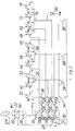
- the circuit of Fig. 2 has 15 input lines which are identified as PP1, PP2, . . . . , PP15. Each of these input lines is considered to have a binary one thereon when the voltage on that line is low.
- Each of the input lines, such as PP1 is connected to the gate of a P-type transistor 20.
- the source of each P-type transistor, such as transistor 20, has its source connected to a positive supply as illustrated at 22.
- the drains of all the transistors 20 are connected together by a single line 24 which constitutes a summing node for adding all the currents produced by the P-type transistors .
- a P-type transistor 21 has its source connected to a positive supply, its gate to ground and its drain coupled to line 24. Transistor 20 always conducts 0.5i0 so that the minimum current in line 24 is 0.5i0 which occurs whenever all the inputs PP1 - PP15 are zero or high.
- Each of the transistors 20 coupled to one of the 15 input lines is sized so that when the input line coupled thereto has a low voltage thereon signifying a binary one input, the current conducted by the transistor 20 is i0. Accordingly, when signals are applied to the input lines PP1 - PP15, the current I 1 flowing in line 24 ranges from 0.5i0, when all input lines are at a zero level (high), to 15.5i0, when all input lines are at a one level (high).
- the inputs comprise the binary inputs from the columns, such as column 26 or 28 in Fig. 1.
- the topmost bit in column 26, for example, would be connected to the input line PP1 in Fig. 2.
- the second bit in the column 26, would be connected to the input line PP2. Since the column 26 has only 8 rows, the eighth bit in the column would connect to PP8.
- the resultant sum bit from the current mode circuit for column 26 is bit 30 which appears at the output labeled SUM in Fig. 2.
- a second circuit of the type shown in Fig. 2 would be utilized to form the sum of the bits in column 28.
- the line 24 is coupled to the drain and the source of a transistor 30.
- the source of transistor 30 is coupled to ground.
- the configuration of transistors 30, 34, 54, 68 and 80 comprises a well known current mirror.
- the circuit includes a first current source which comprises a P-type transistor 32 having its gate coupled to ground and its source coupled to a positive voltage source.
- This transistor is specially designed to conduct 8i0 of current.
- One convenient approach to producing such a transistor is to replicate transistor 20, which will conduct i0, eight times and connecting these transistors in parallel.
- the drain of the transistor 32 is coupled to the drain of N-type transistor 34 and the input to inverter 36.
- the source of transistor 34 is connected to ground while the gate thereof is connected to node S1.
- the transistor 34 is identical to transistor 30 and attempts to mirror the current I 1 although transistor 32 will limit the maximum current through transistor 34 to 8i0.
- node 38 When the current I 1 is less than 8i0, node 38 is high.
- the voltage at node 38 is low.
- the low voltage at node 38 is inverted by two series connected inverters 36 and 36' to produce at node 40 a low level signal which is coupled to P-type transistors 42, 44 and 46.
- transistors 32 and 34 as configured comprise a circuit for detecting when the current I 1 is 8i0 or greater and producing a low level signal at 40 indicating this condition.
- the signal at 40 accordingly, is the high order sum bit for the data bits input to circuit of Fig. 2.
- the signal at node 40 comprises C3OUT which is a carry out signal which needs to be added to the bits in the column 3 bit positions to the left of the column in which it was generated.
- this adding of carry bits to the data in other columns greatly complicates the complexity of the design layout.
- the carry bits are simply added as another input to the data being added in another column. This aspect of the invention will be described more fully in connection with Fig. 5.
- the signal indicating whether the current I 1 is greater than or equal to 8i0 at 40 is coupled to transistor 42.
- P-type transistor 42 When the signal at 40 is low (indicating the current I 1 is equal to or greater than 8i0), P-type transistor 42 is conductive. This transistor is sized so that when it conducts it will conduct 8i0 current into node 50. Such a transistor can be designed or produced by replicating eight transistors such as transistor 20 and connecting them in parallel. An additional P-type transistor 52 also conducts 4i0 current into node 50. This transistor 52 can be made by design or replication as already noted.
- Node 50 connects to the drain of N-type transistor 54 and the input to inverter 56. The source of transistor 54 couples to ground and the gate thereof couples to node S1.
- the transistor 54 is the same as transistor 30.
- the transistors 42, 52 and 54 are interoperative to detect when the current I 1 is greater than 12i0 or between 4i0 and 7i0. This condition is indicated by a low level at node 50 which is coupled to the series connected inverters 56 and 56' to form a low signal at node 58.
- This signal at 58 comprises the second order sum bit for the data bits input to the circuit of Fig. 2. It also comprises a carry out C2OUT signal used in a Wallace tree multiplier and is added to the bits in the column two bit positions to the left of the column in which it was generated.
- Node 58 couples to the gate of P-type transistors 60 and 62. These transistors 60 and 62 have their sources coupled to a positive supply.
- the drain of transistor 60 couples to a node 64 as do the drains of transistors 44 and 66.
- Transistors 44, 60 and 66 are respectively designed to conduct 8i0, 4i0 and 2i0 current when they are conductive and can be made by design or replication.
- Transistor 66 is always conductive because its gate is grounded.
- Transistor 44 conducts only when the highest order sum bit is a one and transistor 60 conducts only when the second order sum bit is a one.
- the node 64 couples to the drain of transistor 68.
- the gate of transistor 68 connects to node S1 and the source connects to ground.
- the transistor 68 is identical to transistor 30.
- the node 64 also connects to the input of two series connected inverters 70 and 70'.
- the signal at node 72 is low whenever the third order sum bit for the data bits input to the circuit comprises a one. This signal is used in a Wallace tree multiplier as a carry out signal C1OUT which is added to the bits in the column to the left of the column in which this signal was produced.
- the two series connected inverters 70 and 70' have an output coupled to a node 72 which connects to the gate of P-type transistor 74.
- the source of transistor 74 connects to a positive voltage source and the drain thereof connects to a node 76.
- a further transistor 78 has its gate grounded, its source coupled to a positive voltage source and its drain connected to node 76.
- Transistors 46, 62, 74 and 78 are designed to respectively conduct 8i0, 4i0, 2i0, and 1i0 whenever these transistors are conductive which occurs when their gates are low.
- the current conducted by transistors 46, 62,74, and 78 enters node 76. This node is connected to the drain of N-type transistor 80 and the input to inverter 82.
- the source of transistor 80 couples to ground and its gate couples to node S1.
- the voltage at node 76 is low whenever the lowest order sum bit for the data bits input to the circuit of Fig. 2 comprises a one.
- the inverter 82 produces the lowest order sum bit at its output which comprises a one when the level at the output terminal labeled SUM is high and a zero when the level at the terminal labeled SUM is low.
- Fig. 3 illustrates a circuit generally of the type illustrated in Fig. 2, however, Fig. 3 is a circuit suitable for adding a column containing only 3 binary bits.
- Fig. 2 can be modified to provide a circuit for adding a column of 7 binary bits utilizing the readily apparent approach for modifying that circuit.
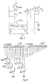
- Fig. 4 illustrates, in part, the manner in which the circuit in Fig. 2 can be coupled into a Wallace tree adder of the type illustrated in Fig. 1.
- the circuit of Fig. 2 can be utilized to perform the sum of the column of binary bits illustrated as column 26.
- the A H is stored in the A operand register 100 which has eight bit positions numbered from 1 to 8.
- the B H operand is stored in the B operand register 102.
- the top most bit in the column 26 is produced by the NAND 104 which has two inputs thereto, the 1 bit from the A operand register 100 and the 8 bit from the B operand register 102.
- the output of NAND gate 104 is PP1 which is an input to the circuit of Fig. 2.
- the second bit position in column 26 is formed by NAND 106 which has two inputs thereto, the 2 bit from the A operand register 100 and the 7 bit from the B operand register 102.
- the output of NAND gate 106 comprises PP2 which is an input to the circuit of Fig. 2.
- the remaining bits in the column 26 of Fig. 1 are formed by the remaining NAND gates illustrated in Fig. 4. As such, all the inputs PP1 through PP8 are produced by the circuit of Fig. 4.
- the circuitry of Fig. 2 is utilized in the portion of the Wallace tree adder of Fig. 5.
- the circuit of Fig. 2 is coupled into the circuit and is illustrated at 120, 122, 124, 126.
- the circuit 120 has 15 inputs thereto, although not all of them will necessarily be used.
- This circuit 120 has its high order bit or C3OUT coupled by line 128 to the PP15 input for the circuit 126 located 3 columns to the left of the first column.
- the second order bit or C2OUT of circuit 120 is coupled by line 130 to the PP15 input to the circuit 124 located two columns to the left of column 1.
- the third order bit or C1OUT of circuit 120 is coupled by line 132 to the PP15 input to circuit 122 located in column 2.
- the high order bits output from the circuits 122, 124 and 126 are coupled to circuits in columns to the left of the column in which they were developed.
- this configuration contributes to the speed of operation of the present invention. It also contributes to an easier circuit layout when the present multiplier is implemented in VLSI.
Landscapes
- Physics & Mathematics (AREA)
- Engineering & Computer Science (AREA)
- General Physics & Mathematics (AREA)
- Mathematical Analysis (AREA)
- Pure & Applied Mathematics (AREA)
- Theoretical Computer Science (AREA)
- Mathematical Optimization (AREA)
- Computational Mathematics (AREA)
- Computing Systems (AREA)
- General Engineering & Computer Science (AREA)
- Mathematical Physics (AREA)
- Algebra (AREA)
- Logic Circuits (AREA)
- Complex Calculations (AREA)
- Image Processing (AREA)
Applications Claiming Priority (2)
| Application Number | Priority Date | Filing Date | Title |
|---|---|---|---|
| US36828895A | 1995-01-03 | 1995-01-03 | |
| US368288 | 1995-01-03 |
Publications (1)
| Publication Number | Publication Date |
|---|---|
| EP0721159A1 true EP0721159A1 (fr) | 1996-07-10 |
Family
ID=23450635
Family Applications (1)
| Application Number | Title | Priority Date | Filing Date |
|---|---|---|---|
| EP95120657A Withdrawn EP0721159A1 (fr) | 1995-01-03 | 1995-12-28 | Additionneur binaire à entrées multiples |
Country Status (4)
| Country | Link |
|---|---|
| EP (1) | EP0721159A1 (fr) |
| JP (1) | JPH08274626A (fr) |
| KR (1) | KR960029957A (fr) |
| TW (1) | TW302454B (fr) |
Cited By (40)
| Publication number | Priority date | Publication date | Assignee | Title |
|---|---|---|---|---|
| US8266199B2 (en) | 2006-02-09 | 2012-09-11 | Altera Corporation | Specialized processing block for programmable logic device |
| US8266198B2 (en) | 2006-02-09 | 2012-09-11 | Altera Corporation | Specialized processing block for programmable logic device |
| US8301681B1 (en) | 2006-02-09 | 2012-10-30 | Altera Corporation | Specialized processing block for programmable logic device |
| US8307023B1 (en) | 2008-10-10 | 2012-11-06 | Altera Corporation | DSP block for implementing large multiplier on a programmable integrated circuit device |
| US8386553B1 (en) | 2006-12-05 | 2013-02-26 | Altera Corporation | Large multiplier for programmable logic device |
| US8386550B1 (en) | 2006-09-20 | 2013-02-26 | Altera Corporation | Method for configuring a finite impulse response filter in a programmable logic device |
| US8396914B1 (en) | 2009-09-11 | 2013-03-12 | Altera Corporation | Matrix decomposition in an integrated circuit device |
| US8412756B1 (en) | 2009-09-11 | 2013-04-02 | Altera Corporation | Multi-operand floating point operations in a programmable integrated circuit device |
| US8468192B1 (en) | 2009-03-03 | 2013-06-18 | Altera Corporation | Implementing multipliers in a programmable integrated circuit device |
| US8484265B1 (en) | 2010-03-04 | 2013-07-09 | Altera Corporation | Angular range reduction in an integrated circuit device |
| US8510354B1 (en) | 2010-03-12 | 2013-08-13 | Altera Corporation | Calculation of trigonometric functions in an integrated circuit device |
| US8539014B2 (en) | 2010-03-25 | 2013-09-17 | Altera Corporation | Solving linear matrices in an integrated circuit device |
| US8539016B1 (en) | 2010-02-09 | 2013-09-17 | Altera Corporation | QR decomposition in an integrated circuit device |
| US8543634B1 (en) | 2012-03-30 | 2013-09-24 | Altera Corporation | Specialized processing block for programmable integrated circuit device |
| US8577951B1 (en) | 2010-08-19 | 2013-11-05 | Altera Corporation | Matrix operations in an integrated circuit device |
| US8589463B2 (en) | 2010-06-25 | 2013-11-19 | Altera Corporation | Calculation of trigonometric functions in an integrated circuit device |
| US8601044B2 (en) | 2010-03-02 | 2013-12-03 | Altera Corporation | Discrete Fourier Transform in an integrated circuit device |
| US8620980B1 (en) | 2005-09-27 | 2013-12-31 | Altera Corporation | Programmable device with specialized multiplier blocks |
| US8645450B1 (en) | 2007-03-02 | 2014-02-04 | Altera Corporation | Multiplier-accumulator circuitry and methods |
| US8645449B1 (en) | 2009-03-03 | 2014-02-04 | Altera Corporation | Combined floating point adder and subtractor |
| US8645451B2 (en) | 2011-03-10 | 2014-02-04 | Altera Corporation | Double-clocked specialized processing block in an integrated circuit device |
| US8650236B1 (en) | 2009-08-04 | 2014-02-11 | Altera Corporation | High-rate interpolation or decimation filter in integrated circuit device |
| US8650231B1 (en) | 2007-01-22 | 2014-02-11 | Altera Corporation | Configuring floating point operations in a programmable device |
| US8706790B1 (en) | 2009-03-03 | 2014-04-22 | Altera Corporation | Implementing mixed-precision floating-point operations in a programmable integrated circuit device |
| US8762443B1 (en) | 2011-11-15 | 2014-06-24 | Altera Corporation | Matrix operations in an integrated circuit device |
| US8788562B2 (en) | 2006-12-05 | 2014-07-22 | Altera Corporation | Large multiplier for programmable logic device |
| US8812576B1 (en) | 2011-09-12 | 2014-08-19 | Altera Corporation | QR decomposition in an integrated circuit device |
| US8862650B2 (en) | 2010-06-25 | 2014-10-14 | Altera Corporation | Calculation of trigonometric functions in an integrated circuit device |
| US8949298B1 (en) | 2011-09-16 | 2015-02-03 | Altera Corporation | Computing floating-point polynomials in an integrated circuit device |
| US8959137B1 (en) | 2008-02-20 | 2015-02-17 | Altera Corporation | Implementing large multipliers in a programmable integrated circuit device |
| US8996600B1 (en) | 2012-08-03 | 2015-03-31 | Altera Corporation | Specialized processing block for implementing floating-point multiplier with subnormal operation support |
| US9053045B1 (en) | 2011-09-16 | 2015-06-09 | Altera Corporation | Computing floating-point polynomials in an integrated circuit device |
| TWI489375B (zh) * | 2010-12-03 | 2015-06-21 | Via Tech Inc | 無進位乘法裝置及其處理方法 |
| US9098332B1 (en) | 2012-06-01 | 2015-08-04 | Altera Corporation | Specialized processing block with fixed- and floating-point structures |
| US9189200B1 (en) | 2013-03-14 | 2015-11-17 | Altera Corporation | Multiple-precision processing block in a programmable integrated circuit device |
| US9207909B1 (en) | 2012-11-26 | 2015-12-08 | Altera Corporation | Polynomial calculations optimized for programmable integrated circuit device structures |
| US9348795B1 (en) | 2013-07-03 | 2016-05-24 | Altera Corporation | Programmable device using fixed and configurable logic to implement floating-point rounding |
| US9600278B1 (en) | 2011-05-09 | 2017-03-21 | Altera Corporation | Programmable device using fixed and configurable logic to implement recursive trees |
| US9684488B2 (en) | 2015-03-26 | 2017-06-20 | Altera Corporation | Combined adder and pre-adder for high-radix multiplier circuit |
| US10942706B2 (en) | 2017-05-05 | 2021-03-09 | Intel Corporation | Implementation of floating-point trigonometric functions in an integrated circuit device |
Citations (3)
| Publication number | Priority date | Publication date | Assignee | Title |
|---|---|---|---|---|
| FR2469836A1 (fr) * | 1979-11-16 | 1981-05-22 | Hennion Bernard | Systeme de codage et decodage a multiniveaux en courant |
| FR2560409A1 (fr) * | 1984-02-28 | 1985-08-30 | Lardy Jean Louis | Unite arithmetique pour additionner des bits paralleles |
| FR2599528A1 (fr) * | 1986-05-29 | 1987-12-04 | Centre Nat Rech Scient | Additionneur bipolaire et multiplieur binaire bipolaire comprenant au moins un tel additionneur |
Family Cites Families (5)
| Publication number | Priority date | Publication date | Assignee | Title |
|---|---|---|---|---|
| US5153848A (en) * | 1988-06-17 | 1992-10-06 | Bipolar Integrated Technology, Inc. | Floating point processor with internal free-running clock |
| KR920006323B1 (ko) * | 1990-05-31 | 1992-08-03 | 삼성전자 주식회사 | 스킵(Skip)배열과 수정형 월리스(Wallace)트리를 사용하는 병렬 승산기 |
| US5265043A (en) * | 1991-12-23 | 1993-11-23 | Motorola, Inc. | Wallace tree multiplier array having an improved layout topology |
| US5257217A (en) * | 1992-05-01 | 1993-10-26 | Seiko Epson Corporation | Area-efficient multiplier for use in an integrated circuit |
| US5343417A (en) * | 1992-11-20 | 1994-08-30 | Unisys Corporation | Fast multiplier |
-
1995
- 1995-12-28 EP EP95120657A patent/EP0721159A1/fr not_active Withdrawn
- 1995-12-29 KR KR1019950067687A patent/KR960029957A/ko not_active Application Discontinuation
-
1996
- 1996-01-04 JP JP8000114A patent/JPH08274626A/ja active Pending
- 1996-03-04 TW TW085102585A patent/TW302454B/zh active
Patent Citations (3)
| Publication number | Priority date | Publication date | Assignee | Title |
|---|---|---|---|---|
| FR2469836A1 (fr) * | 1979-11-16 | 1981-05-22 | Hennion Bernard | Systeme de codage et decodage a multiniveaux en courant |
| FR2560409A1 (fr) * | 1984-02-28 | 1985-08-30 | Lardy Jean Louis | Unite arithmetique pour additionner des bits paralleles |
| FR2599528A1 (fr) * | 1986-05-29 | 1987-12-04 | Centre Nat Rech Scient | Additionneur bipolaire et multiplieur binaire bipolaire comprenant au moins un tel additionneur |
Non-Patent Citations (1)
| Title |
|---|
| PELAYO F ET AL: "SOME IMPROVEMENTS IN THE IMPLEMENTATION OF MULTITHRESHOLD AND MULTIVALUED I2L CIRCUITS", INTERNATIONAL JOURNAL OF ELECTRONICS, vol. 66, no. 1, 1 January 1989 (1989-01-01), pages 19 - 34, XP000111343 * |
Cited By (43)
| Publication number | Priority date | Publication date | Assignee | Title |
|---|---|---|---|---|
| US8620980B1 (en) | 2005-09-27 | 2013-12-31 | Altera Corporation | Programmable device with specialized multiplier blocks |
| US8266199B2 (en) | 2006-02-09 | 2012-09-11 | Altera Corporation | Specialized processing block for programmable logic device |
| US8266198B2 (en) | 2006-02-09 | 2012-09-11 | Altera Corporation | Specialized processing block for programmable logic device |
| US8301681B1 (en) | 2006-02-09 | 2012-10-30 | Altera Corporation | Specialized processing block for programmable logic device |
| US8386550B1 (en) | 2006-09-20 | 2013-02-26 | Altera Corporation | Method for configuring a finite impulse response filter in a programmable logic device |
| US9063870B1 (en) | 2006-12-05 | 2015-06-23 | Altera Corporation | Large multiplier for programmable logic device |
| US8788562B2 (en) | 2006-12-05 | 2014-07-22 | Altera Corporation | Large multiplier for programmable logic device |
| US8386553B1 (en) | 2006-12-05 | 2013-02-26 | Altera Corporation | Large multiplier for programmable logic device |
| US9395953B2 (en) | 2006-12-05 | 2016-07-19 | Altera Corporation | Large multiplier for programmable logic device |
| US8650231B1 (en) | 2007-01-22 | 2014-02-11 | Altera Corporation | Configuring floating point operations in a programmable device |
| US8645450B1 (en) | 2007-03-02 | 2014-02-04 | Altera Corporation | Multiplier-accumulator circuitry and methods |
| US8959137B1 (en) | 2008-02-20 | 2015-02-17 | Altera Corporation | Implementing large multipliers in a programmable integrated circuit device |
| US8307023B1 (en) | 2008-10-10 | 2012-11-06 | Altera Corporation | DSP block for implementing large multiplier on a programmable integrated circuit device |
| US8468192B1 (en) | 2009-03-03 | 2013-06-18 | Altera Corporation | Implementing multipliers in a programmable integrated circuit device |
| US8645449B1 (en) | 2009-03-03 | 2014-02-04 | Altera Corporation | Combined floating point adder and subtractor |
| US8706790B1 (en) | 2009-03-03 | 2014-04-22 | Altera Corporation | Implementing mixed-precision floating-point operations in a programmable integrated circuit device |
| US8650236B1 (en) | 2009-08-04 | 2014-02-11 | Altera Corporation | High-rate interpolation or decimation filter in integrated circuit device |
| US8412756B1 (en) | 2009-09-11 | 2013-04-02 | Altera Corporation | Multi-operand floating point operations in a programmable integrated circuit device |
| US8396914B1 (en) | 2009-09-11 | 2013-03-12 | Altera Corporation | Matrix decomposition in an integrated circuit device |
| US8539016B1 (en) | 2010-02-09 | 2013-09-17 | Altera Corporation | QR decomposition in an integrated circuit device |
| US8601044B2 (en) | 2010-03-02 | 2013-12-03 | Altera Corporation | Discrete Fourier Transform in an integrated circuit device |
| US8484265B1 (en) | 2010-03-04 | 2013-07-09 | Altera Corporation | Angular range reduction in an integrated circuit device |
| US8510354B1 (en) | 2010-03-12 | 2013-08-13 | Altera Corporation | Calculation of trigonometric functions in an integrated circuit device |
| US8539014B2 (en) | 2010-03-25 | 2013-09-17 | Altera Corporation | Solving linear matrices in an integrated circuit device |
| US8862650B2 (en) | 2010-06-25 | 2014-10-14 | Altera Corporation | Calculation of trigonometric functions in an integrated circuit device |
| US8589463B2 (en) | 2010-06-25 | 2013-11-19 | Altera Corporation | Calculation of trigonometric functions in an integrated circuit device |
| US8812573B2 (en) | 2010-06-25 | 2014-08-19 | Altera Corporation | Calculation of trigonometric functions in an integrated circuit device |
| US8577951B1 (en) | 2010-08-19 | 2013-11-05 | Altera Corporation | Matrix operations in an integrated circuit device |
| TWI489375B (zh) * | 2010-12-03 | 2015-06-21 | Via Tech Inc | 無進位乘法裝置及其處理方法 |
| US8645451B2 (en) | 2011-03-10 | 2014-02-04 | Altera Corporation | Double-clocked specialized processing block in an integrated circuit device |
| US9600278B1 (en) | 2011-05-09 | 2017-03-21 | Altera Corporation | Programmable device using fixed and configurable logic to implement recursive trees |
| US8812576B1 (en) | 2011-09-12 | 2014-08-19 | Altera Corporation | QR decomposition in an integrated circuit device |
| US9053045B1 (en) | 2011-09-16 | 2015-06-09 | Altera Corporation | Computing floating-point polynomials in an integrated circuit device |
| US8949298B1 (en) | 2011-09-16 | 2015-02-03 | Altera Corporation | Computing floating-point polynomials in an integrated circuit device |
| US8762443B1 (en) | 2011-11-15 | 2014-06-24 | Altera Corporation | Matrix operations in an integrated circuit device |
| US8543634B1 (en) | 2012-03-30 | 2013-09-24 | Altera Corporation | Specialized processing block for programmable integrated circuit device |
| US9098332B1 (en) | 2012-06-01 | 2015-08-04 | Altera Corporation | Specialized processing block with fixed- and floating-point structures |
| US8996600B1 (en) | 2012-08-03 | 2015-03-31 | Altera Corporation | Specialized processing block for implementing floating-point multiplier with subnormal operation support |
| US9207909B1 (en) | 2012-11-26 | 2015-12-08 | Altera Corporation | Polynomial calculations optimized for programmable integrated circuit device structures |
| US9189200B1 (en) | 2013-03-14 | 2015-11-17 | Altera Corporation | Multiple-precision processing block in a programmable integrated circuit device |
| US9348795B1 (en) | 2013-07-03 | 2016-05-24 | Altera Corporation | Programmable device using fixed and configurable logic to implement floating-point rounding |
| US9684488B2 (en) | 2015-03-26 | 2017-06-20 | Altera Corporation | Combined adder and pre-adder for high-radix multiplier circuit |
| US10942706B2 (en) | 2017-05-05 | 2021-03-09 | Intel Corporation | Implementation of floating-point trigonometric functions in an integrated circuit device |
Also Published As
| Publication number | Publication date |
|---|---|
| TW302454B (fr) | 1997-04-11 |
| KR960029957A (ko) | 1996-08-17 |
| JPH08274626A (ja) | 1996-10-18 |
Similar Documents
| Publication | Publication Date | Title |
|---|---|---|
| EP0721159A1 (fr) | Additionneur binaire à entrées multiples | |
| US6523055B1 (en) | Circuit and method for multiplying and accumulating the sum of two products in a single cycle | |
| US5465226A (en) | High speed digital parallel multiplier | |
| Lim | Single-precision multiplier with reduced circuit complexity for signal processing applications | |
| Maley et al. | The logic design of transistor digital computers | |
| Kameyama et al. | A multiplier chip with multiple-valued bidirectional current-mode logic circuits | |
| JP3244506B2 (ja) | 小型乗算器 | |
| US20040024804A1 (en) | Linear summation multiplier array implementation for both signed and unsigned multiplication | |
| Kinniment | An evaluation of asynchronous addition | |
| US5070471A (en) | High speed multiplier which divides multiplying factor into parts and adds partial end products | |
| Gandhi et al. | Comparative analysis for hardware circuit architecture of Wallace tree multiplier | |
| EP0147296B1 (fr) | Circuit de multiplication | |
| Johnson | A digital quarter square multiplier | |
| US8417761B2 (en) | Direct decimal number tripling in binary coded adders | |
| US5132921A (en) | High speed digital computing system | |
| US20030065700A1 (en) | High-performance adder | |
| Maden et al. | Parallel architectures for high speed multipliers | |
| Stepchenkov et al. | Self-timed multiply-add-subtract unit alternates | |
| EP0112186B1 (fr) | Multiplicateurs modulaires à grande vitesse, et modules de circuits intégrés pour de tels multiplicateurs | |
| US5544084A (en) | Multiplier composed of integrated semiconductor circuit occupying reduced area | |
| Elguibaly | Overflow handling in inner-product processors | |
| Abid et al. | Modified operand decomposition multiplication for high performance parallel multipliers | |
| US6631393B1 (en) | Method and apparatus for speculative addition using a limited carry | |
| Thornton | A signed binary addition circuit based on an alternative class of addition tables | |
| US5034912A (en) | Signal processing circuit for multiplication |
Legal Events
| Date | Code | Title | Description |
|---|---|---|---|
| PUAI | Public reference made under article 153(3) epc to a published international application that has entered the european phase |
Free format text: ORIGINAL CODE: 0009012 |
|
| AK | Designated contracting states |
Kind code of ref document: A1 Designated state(s): DE FR GB IT NL |
|
| 17P | Request for examination filed |
Effective date: 19970108 |
|
| 17Q | First examination report despatched |
Effective date: 20000720 |
|
| STAA | Information on the status of an ep patent application or granted ep patent |
Free format text: STATUS: THE APPLICATION IS DEEMED TO BE WITHDRAWN |
|
| 18D | Application deemed to be withdrawn |
Effective date: 20010331 |