EP0720280B1 - Dispositif électronique de conversion de l'énergie électrique et installation en faisant usage - Google Patents
Dispositif électronique de conversion de l'énergie électrique et installation en faisant usage Download PDFInfo
- Publication number
- EP0720280B1 EP0720280B1 EP95402961A EP95402961A EP0720280B1 EP 0720280 B1 EP0720280 B1 EP 0720280B1 EP 95402961 A EP95402961 A EP 95402961A EP 95402961 A EP95402961 A EP 95402961A EP 0720280 B1 EP0720280 B1 EP 0720280B1
- Authority
- EP
- European Patent Office
- Prior art keywords
- voltage
- converter
- cell
- switches
- voltage source
- Prior art date
- Legal status (The legal status is an assumption and is not a legal conclusion. Google has not performed a legal analysis and makes no representation as to the accuracy of the status listed.)
- Expired - Lifetime
Links
Images
Classifications
-
- H—ELECTRICITY
- H02—GENERATION; CONVERSION OR DISTRIBUTION OF ELECTRIC POWER
- H02M—APPARATUS FOR CONVERSION BETWEEN AC AND AC, BETWEEN AC AND DC, OR BETWEEN DC AND DC, AND FOR USE WITH MAINS OR SIMILAR POWER SUPPLY SYSTEMS; CONVERSION OF DC OR AC INPUT POWER INTO SURGE OUTPUT POWER; CONTROL OR REGULATION THEREOF
- H02M7/00—Conversion of ac power input into dc power output; Conversion of dc power input into ac power output
- H02M7/02—Conversion of ac power input into dc power output without possibility of reversal
- H02M7/04—Conversion of ac power input into dc power output without possibility of reversal by static converters
- H02M7/12—Conversion of ac power input into dc power output without possibility of reversal by static converters using discharge tubes with control electrode or semiconductor devices with control electrode
- H02M7/145—Conversion of ac power input into dc power output without possibility of reversal by static converters using discharge tubes with control electrode or semiconductor devices with control electrode using devices of a thyratron or thyristor type requiring extinguishing means
- H02M7/155—Conversion of ac power input into dc power output without possibility of reversal by static converters using discharge tubes with control electrode or semiconductor devices with control electrode using devices of a thyratron or thyristor type requiring extinguishing means using semiconductor devices only
- H02M7/17—Conversion of ac power input into dc power output without possibility of reversal by static converters using discharge tubes with control electrode or semiconductor devices with control electrode using devices of a thyratron or thyristor type requiring extinguishing means using semiconductor devices only arranged for operation in parallel
-
- H—ELECTRICITY
- H02—GENERATION; CONVERSION OR DISTRIBUTION OF ELECTRIC POWER
- H02M—APPARATUS FOR CONVERSION BETWEEN AC AND AC, BETWEEN AC AND DC, OR BETWEEN DC AND DC, AND FOR USE WITH MAINS OR SIMILAR POWER SUPPLY SYSTEMS; CONVERSION OF DC OR AC INPUT POWER INTO SURGE OUTPUT POWER; CONTROL OR REGULATION THEREOF
- H02M7/00—Conversion of ac power input into dc power output; Conversion of dc power input into ac power output
- H02M7/42—Conversion of dc power input into ac power output without possibility of reversal
- H02M7/44—Conversion of dc power input into ac power output without possibility of reversal by static converters
- H02M7/48—Conversion of dc power input into ac power output without possibility of reversal by static converters using discharge tubes with control electrode or semiconductor devices with control electrode
- H02M7/483—Converters with outputs that each can have more than two voltages levels
-
- H—ELECTRICITY
- H02—GENERATION; CONVERSION OR DISTRIBUTION OF ELECTRIC POWER
- H02M—APPARATUS FOR CONVERSION BETWEEN AC AND AC, BETWEEN AC AND DC, OR BETWEEN DC AND DC, AND FOR USE WITH MAINS OR SIMILAR POWER SUPPLY SYSTEMS; CONVERSION OF DC OR AC INPUT POWER INTO SURGE OUTPUT POWER; CONTROL OR REGULATION THEREOF
- H02M7/00—Conversion of ac power input into dc power output; Conversion of dc power input into ac power output
- H02M7/42—Conversion of dc power input into ac power output without possibility of reversal
- H02M7/44—Conversion of dc power input into ac power output without possibility of reversal by static converters
- H02M7/48—Conversion of dc power input into ac power output without possibility of reversal by static converters using discharge tubes with control electrode or semiconductor devices with control electrode
- H02M7/483—Converters with outputs that each can have more than two voltages levels
- H02M7/4837—Flying capacitor converters
Definitions
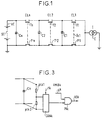
- the present invention relates to devices electrical power conversion electronics of the type described in patent application FR - 2 679 715 A1 and a power installation making use of it.
- the converter described in this patent application is illustrated, by way of example, in FIG. 1 appended hereto. It essentially comprises, between a voltage source SE and a current source C, a succession of cells of controllable switching CL1, CL2 ..., CLn, each having two switches T1, T'1; T2, T'2 ...; Tn, T'n, with a pole of each of the two switches constituting a pair of upstream poles and the other pole of each of the switches constituting a pair of downstream poles, the pair of downstream poles an upstream cell being connected to the pair of poles upstream of a downstream cell and the pair of poles upstream of a first cell CL1 being connected to said source of current C, while the downstream pole pair of a last cell CLn is connected to said voltage source SE, this converter further comprising a capacitor C1, C2 ..., Cn, for each cell, except that of the last one can be omitted when said voltage source SE is able to play the role, connected between the two poles of the pair of downstream poles
- said fraction of period is equal to the inverse of the number n of cells, i.e. 2 ⁇ / n, which is optimal with regard to the harmonics generated on the output and allows natural balancing of the voltages charging of converter capacitors. Another shift is however conceivable.
- converter multilevel a converter corresponding to the description which precedes.
- the object of the present invention is to ensure that that said capacitors respectively acquire said nominal charge voltages, quickly, as soon as said voltage source supplies the converter.
- the operating principle of converter is such that if the nominal charging voltage of a capacitor is higher than it should be, this one supplies more current to the source of current, which tends to bring its charge voltage back to its nominal value.
- this process is relatively slow, especially when the current in the source of current is weak. Applied to conditions where said source initially inactive, suddenly establishes the converter supply voltage, this means that, for a relatively long period of time, the switches would be subjected to abnormally high voltages.
- the converter comprises arranged control means to evaluate said voltage of the voltage source and, as soon as when it is below a determined threshold, for suspend said nominal operation of the converter and act on said switches so that when said voltage of the voltage source has a value between zero and a voltage corresponding to the charging voltage nominal nominal load voltage capacitor la lower, it charges all the capacitors of the converter, when this voltage from the voltage source exceeds said lower rated load voltage, the capacitor nominally charged under the latter voltage is switched off, said voltage from the source of voltage continuing to charge voltage capacitors higher nominal loads, when the voltage of the voltage source exceeds the rated load voltage by immediately higher capacitor, the capacitor nominally charged under this latter voltage is at its turn off, and so on, until all converter capacitors are charged under their respective nominal charge voltages, after which said control means establish said operation nominal converter.
- said control means act on said switches so that initially both switches of all cells are closed together, except those in the first cell who are in another state, after which, as the said voltage from the voltage source, both switches of the following successive cells are set in said other state, cell after cell.
- the invention also relates to an installation making use of such a converter and which is fitted, as far as necessary, so that said establishment of the voltage of the voltage source has a progressivity appropriate to the converter used.
- FIG. 1 corresponds to a converter of the type described in the patent document FR - 2 697 715 A1 to which the reader is returned for further details.
- Figure 2 only shows the converter of the Figure 1, that the capacitors C1, C2 ..., Cn.
- Each of these capacitors is associated, according to the invention, an evaluation device VMO1, VMO2 ..., VMOn to assess the voltage across each of the capacitors.
- this device is coupled to two capacitor terminals. It provides a signal VO1, VO2 ..., VOn expressing the existing voltage across the capacitor.
- this device will be composed, according to a form of implementation work, of impedances ptk1 and ptk2, connected in series between the terminals of the capacitor Ck, and providing a fraction determined from the voltage across this capacitor to a ADC providing to each pulse fk a digital voltage value read by a PVk gate circuit triggered by a gk signal.
- the signals fk and gk will advantageously be produced by a base of BT time ( Figure 2).
- Each of the capacitors is also associated, according to the invention, a deviation device VE1, VE2 ..., V
- a deviation device VE1, VE2 ..., V By allowing to note a possible difference between the observed charge voltage, which it receives from the device corresponding evaluation voltage and the nominal charging voltage of this capacitor.
- This deviation reporting system calculates itself the nominal charge voltage of this capacitor, which is the fraction 1 / n, n being the number of stages of the converter, of the voltage VE of the source of voltage SE, multiplied by the row R of the stage.
- This device therefore receives the values VE and R, the value n, constant of the entire converter being wired into each device (the R value, constant of each stage, could also be wired).
- VEC1 deviation signal VEC2 ..., VECn, characterizing the difference between these two tensions.
- VEC1 deviation signal VEC2 ..., VECn
- This deviation signal can be a simple signal logic (two-bit) characterizing only the presence of a gap and its sign.
- a deviation signal is not provided only if the charge difference of the capacitor exceeds a threshold predetermined, wired into the finding device away.
- the control means of FIG. 2 include at in addition to control modules MC1, MC2 ..., MCn operating in response to trigger signals sd1, sd2 ..., sdn.
- the BT time base produces an sd signal, which provides the signal directly sd1 and, thanks to the delay units R2 ..., Rn, signals time-shifted sd2 ..., sdn.
- Control modules MC1, MC2 ..., MCn essentially have the function of produce, during each converter period, a control pulse carrying signals in an active state CT1, CT2 ..., CTn, controlling the switches of the converter.
- the nominal duration of this pulse is in each case mainly determined by the VE value of the voltage supplied by the voltage source and by the level of the voltage to be supplied to the current source. We will not describe no more before this aspect of the converter operation which is outside the scope of the present invention.
- the converter comprises control means, mainly located in the base BT time, according to the embodiment of FIG. 2, continuously receiving an assessment of said blood pressure the voltage source of the converter, in the form of deviation signal VECn, and, as soon as this voltage is below a determined threshold, suspending said nominal converter operation.
- the signal VECn relates to the charging voltage of the capacitor Cn, it is at the same time relating to the voltage of the voltage source. In the practical, or this voltage is present at its nominal value and the nominal operation of the converter must be established, or this tension is not present at its value nominal, its value being such that upon return to normal, without the invention, there could be an overshoot of the operating voltage of the switches, and then the normal operation of the converter must not be to pursue ; this will appear more clearly later.
- CT1 signals, CT2 ..., CTn remain in the inactive state which makes conductors switches T'1, T'2 ..., T'n.
- the device DA1 suppresses the charge control signal DR'1 and the switch T2 is blocked, which interrupts the charging of the capacitor C1, while it continues for the others capacitors.
- This assumption will usually be verified, as it almost always includes a filter that limits the slope current establishment. It can also be a network AC voltage supply and the constants of times encountered are generally of the order of quarter period, i.e. 5 ms at 50 Hz, duration much longer than the period of operation of the converter.
- time constant means such as said establishing the voltage the voltage source has a progressivity appropriate to the converter used.
Landscapes
- Engineering & Computer Science (AREA)
- Power Engineering (AREA)
- Dc-Dc Converters (AREA)
- Inverter Devices (AREA)
- Charge And Discharge Circuits For Batteries Or The Like (AREA)
- Control Of Electric Motors In General (AREA)
- Supply And Distribution Of Alternating Current (AREA)
- Control Of Charge By Means Of Generators (AREA)
- Oscillators With Electromechanical Resonators (AREA)
- Heat-Pump Type And Storage Water Heaters (AREA)
- Analogue/Digital Conversion (AREA)
- Measurement Of Resistance Or Impedance (AREA)
Applications Claiming Priority (2)
| Application Number | Priority Date | Filing Date | Title |
|---|---|---|---|
| FR9415864 | 1994-12-29 | ||
| FR9415864A FR2729014A1 (fr) | 1994-12-29 | 1994-12-29 | Dispositif electronique de conversion de l'energie electrique et installation d'alimentation en faisant usage |
Publications (2)
| Publication Number | Publication Date |
|---|---|
| EP0720280A1 EP0720280A1 (fr) | 1996-07-03 |
| EP0720280B1 true EP0720280B1 (fr) | 1998-11-11 |
Family
ID=9470409
Family Applications (1)
| Application Number | Title | Priority Date | Filing Date |
|---|---|---|---|
| EP95402961A Expired - Lifetime EP0720280B1 (fr) | 1994-12-29 | 1995-12-28 | Dispositif électronique de conversion de l'énergie électrique et installation en faisant usage |
Country Status (16)
| Country | Link |
|---|---|
| US (1) | US5668711A (zh) |
| EP (1) | EP0720280B1 (zh) |
| JP (1) | JP3414748B2 (zh) |
| KR (1) | KR100365253B1 (zh) |
| CN (1) | CN1057410C (zh) |
| AT (1) | ATE173363T1 (zh) |
| AU (1) | AU686921B2 (zh) |
| BR (1) | BR9506902A (zh) |
| CA (1) | CA2183788C (zh) |
| DE (1) | DE69505944T2 (zh) |
| DK (1) | DK0720280T3 (zh) |
| ES (1) | ES2124985T3 (zh) |
| FR (1) | FR2729014A1 (zh) |
| RU (1) | RU2138111C1 (zh) |
| TW (1) | TW336360B (zh) |
| WO (1) | WO1996021267A1 (zh) |
Families Citing this family (11)
| Publication number | Priority date | Publication date | Assignee | Title |
|---|---|---|---|---|
| FR2752343B1 (fr) * | 1996-08-09 | 1998-09-11 | Gec Alsthom Transport Sa | Dispositif electronique de conversion de l'energie electrique |
| FR2758020B1 (fr) * | 1996-12-30 | 1999-02-26 | Alsthom Cge Alcatel | Moyens de commande de convertisseur d'energie electrique a niveaux multiples, dit convertisseur multiniveaux |
| FR2809548B1 (fr) * | 2000-05-26 | 2002-08-02 | Centre Nat Rech Scient | Dispositif de conversion d'energie multicellulaire |
| DE10037379B4 (de) * | 2000-08-01 | 2005-06-16 | Alstom | Modular aufgebauter Stromrichter |
| SE517063C2 (sv) * | 2000-08-10 | 2002-04-09 | Abb Ab | Förfarande samt anordning för spänningssättning av en VSC- strömriktare |
| JP3757219B2 (ja) * | 2003-06-27 | 2006-03-22 | 東光株式会社 | チャージポンプ回路 |
| PL2122817T3 (pl) * | 2007-01-17 | 2018-06-29 | Siemens Aktiengesellschaft | Sterowanie gałęzią modułu fazowego wielopoziomowego przekształtnika |
| CA2716022C (en) | 2010-09-30 | 2019-03-12 | Light-Based Technologies Incorporated | Apparatus and methods for supplying power |
| RU2523332C1 (ru) * | 2010-12-13 | 2014-07-20 | Абб Текнолоджи Лтд. | Многоуровневый преобразователь напряжения |
| DE112015001260T5 (de) * | 2014-03-14 | 2016-12-08 | Arctic Sand Technologies, Inc. | Ladungspumpenstabilitätssteuerung |
| DE102015000551A1 (de) | 2015-01-20 | 2016-07-21 | Dürr Systems GmbH | Rotationszerstäuberturbine |
Family Cites Families (8)
| Publication number | Priority date | Publication date | Assignee | Title |
|---|---|---|---|---|
| JPH02215154A (ja) * | 1989-02-16 | 1990-08-28 | Toshiba Corp | 電圧制御回路 |
| GB2245112A (en) * | 1990-06-13 | 1991-12-18 | Philips Electronic Associated | Dc/dc voltage multiplier. |
| FR2679315B1 (fr) * | 1991-07-15 | 1993-10-08 | Bradleigh Weiss | Double travelling asservi assurant le deplacement regulier et commande d'un support sur certaines surfaces reglees. |
| FR2679715B1 (fr) * | 1991-07-25 | 1993-10-29 | Centre Nal Recherc Scientifique | Dispositif electronique de conversion d'energie electrique. |
| JPH0828965B2 (ja) * | 1992-09-02 | 1996-03-21 | 日本電気株式会社 | 電圧変換回路 |
| US5345376A (en) * | 1993-02-19 | 1994-09-06 | Tescom Corporation | Switching power supply with electronic isolation |
| US5568035A (en) * | 1993-10-15 | 1996-10-22 | Sony/Tektronix Corporation | Variable-capacitance power supply apparatus |
| US5491623A (en) * | 1994-09-23 | 1996-02-13 | Fluke Corporation | Voltage multiplier using switched capacitance technique |
-
1994
- 1994-12-29 FR FR9415864A patent/FR2729014A1/fr active Granted
-
1995
- 1995-12-28 KR KR1019960704731A patent/KR100365253B1/ko not_active IP Right Cessation
- 1995-12-28 US US08/676,393 patent/US5668711A/en not_active Expired - Lifetime
- 1995-12-28 CN CN95191773A patent/CN1057410C/zh not_active Expired - Lifetime
- 1995-12-28 CA CA002183788A patent/CA2183788C/fr not_active Expired - Lifetime
- 1995-12-28 JP JP52077196A patent/JP3414748B2/ja not_active Expired - Fee Related
- 1995-12-28 DK DK95402961T patent/DK0720280T3/da active
- 1995-12-28 DE DE69505944T patent/DE69505944T2/de not_active Expired - Lifetime
- 1995-12-28 RU RU96119346A patent/RU2138111C1/ru active
- 1995-12-28 EP EP95402961A patent/EP0720280B1/fr not_active Expired - Lifetime
- 1995-12-28 AT AT95402961T patent/ATE173363T1/de active
- 1995-12-28 ES ES95402961T patent/ES2124985T3/es not_active Expired - Lifetime
- 1995-12-28 BR BR9506902A patent/BR9506902A/pt not_active IP Right Cessation
- 1995-12-28 WO PCT/FR1995/001748 patent/WO1996021267A1/fr active Application Filing
- 1995-12-28 AU AU44523/96A patent/AU686921B2/en not_active Ceased
-
1996
- 1996-02-14 TW TW085101844A patent/TW336360B/zh not_active IP Right Cessation
Also Published As
| Publication number | Publication date |
|---|---|
| AU686921B2 (en) | 1998-02-12 |
| JP3414748B2 (ja) | 2003-06-09 |
| JPH09510078A (ja) | 1997-10-07 |
| EP0720280A1 (fr) | 1996-07-03 |
| DK0720280T3 (da) | 1999-07-26 |
| ATE173363T1 (de) | 1998-11-15 |
| DE69505944T2 (de) | 2000-08-31 |
| AU4452396A (en) | 1996-07-24 |
| KR970701445A (ko) | 1997-03-17 |
| CA2183788A1 (fr) | 1996-07-11 |
| WO1996021267A1 (fr) | 1996-07-11 |
| FR2729014A1 (fr) | 1996-07-05 |
| CN1141696A (zh) | 1997-01-29 |
| FR2729014B1 (zh) | 1997-02-07 |
| BR9506902A (pt) | 1997-09-09 |
| DE69505944D1 (de) | 1998-12-17 |
| RU2138111C1 (ru) | 1999-09-20 |
| KR100365253B1 (ko) | 2003-03-29 |
| US5668711A (en) | 1997-09-16 |
| CN1057410C (zh) | 2000-10-11 |
| TW336360B (en) | 1998-07-11 |
| ES2124985T3 (es) | 1999-02-16 |
| CA2183788C (fr) | 2003-12-23 |
Similar Documents
| Publication | Publication Date | Title |
|---|---|---|
| EP0823772B1 (fr) | Dispositif électronique de conversion de l'énergie électrique | |
| EP0720280B1 (fr) | Dispositif électronique de conversion de l'énergie électrique et installation en faisant usage | |
| EP0377388B1 (fr) | Générateur de forme d'onde de signal analogique | |
| EP2718976B1 (fr) | Batterie photovoltaïque avec architecture en briques disposees en serie ou en parallele | |
| EP0720281B1 (fr) | Dispositif électronique de conversion de l'énergie électrique | |
| EP2944008B1 (fr) | Équilibrage de charge dans une batterie électrique | |
| FR2694978A1 (fr) | Système de mesure d'impédance de batteries en ligne. | |
| FR2769144A1 (fr) | Accumulateur d'electricite | |
| CA3102416A1 (fr) | Systeme electrique a cellules commutees et procede de commande d'un tel systeme | |
| FR2962864A1 (fr) | Dispositif d'equilibrage de la tension aux bornes d'un condensateur d'un ensemble de condensateurs, et systeme de conversion de tension comportant un tel dispositif d'equilibrage | |
| CA2189692C (fr) | Dispositif electronique de conversion de l'energie electrique | |
| EP0851568B1 (fr) | Dispositif électrique de conversion de l'énergie électrique | |
| EP0720282B1 (fr) | Dispositif électronique de conversion de l'énergie électrique et installation d'alimentation en faisant usage | |
| CA2409937C (fr) | Dispositif de conversion d'energie multicellulaire | |
| EP1410488B1 (fr) | Dispositif de conversion d'energie | |
| FR2899039A1 (fr) | Procede et dispositif de conversion d'une tension continue en une tension variable de forme predeterminee,et onduleur dote d'un tel dispositif | |
| FR2861918A1 (fr) | Onduleur cellulaire a taux reduit de distorsions de commutation | |
| WO2014053559A1 (fr) | Procede de regulation d'un micro-onduleur | |
| EP2717459A1 (fr) | Convertisseur CC/CA avec tension intermédiaire sinusoïdale redressée décalée et fonctionnement onduleur MLI |
Legal Events
| Date | Code | Title | Description |
|---|---|---|---|
| PUAI | Public reference made under article 153(3) epc to a published international application that has entered the european phase |
Free format text: ORIGINAL CODE: 0009012 |
|
| AK | Designated contracting states |
Kind code of ref document: A1 Designated state(s): AT BE CH DE DK ES GB IE IT LI LU NL PT SE |
|
| 17P | Request for examination filed |
Effective date: 19961212 |
|
| GRAG | Despatch of communication of intention to grant |
Free format text: ORIGINAL CODE: EPIDOS AGRA |
|
| 17Q | First examination report despatched |
Effective date: 19971205 |
|
| GRAG | Despatch of communication of intention to grant |
Free format text: ORIGINAL CODE: EPIDOS AGRA |
|
| GRAH | Despatch of communication of intention to grant a patent |
Free format text: ORIGINAL CODE: EPIDOS IGRA |
|
| GRAH | Despatch of communication of intention to grant a patent |
Free format text: ORIGINAL CODE: EPIDOS IGRA |
|
| GRAA | (expected) grant |
Free format text: ORIGINAL CODE: 0009210 |
|
| AK | Designated contracting states |
Kind code of ref document: B1 Designated state(s): AT BE CH DE DK ES GB IE IT LI LU NL PT SE |
|
| REF | Corresponds to: |
Ref document number: 173363 Country of ref document: AT Date of ref document: 19981115 Kind code of ref document: T |
|
| REG | Reference to a national code |
Ref country code: CH Ref legal event code: EP |
|
| REF | Corresponds to: |
Ref document number: 69505944 Country of ref document: DE Date of ref document: 19981217 |
|
| REG | Reference to a national code |
Ref country code: IE Ref legal event code: FG4D Free format text: FRENCH |
|
| ITF | It: translation for a ep patent filed |
Owner name: JACOBACCI & PERANI S.P.A. |
|
| REG | Reference to a national code |
Ref country code: ES Ref legal event code: FG2A Ref document number: 2124985 Country of ref document: ES Kind code of ref document: T3 |
|
| GBT | Gb: translation of ep patent filed (gb section 77(6)(a)/1977) |
Effective date: 19990301 |
|
| REG | Reference to a national code |
Ref country code: CH Ref legal event code: NV Representative=s name: CABINET ROLAND NITHARDT CONSEILS EN PROPRIETE INDU |
|
| REG | Reference to a national code |
Ref country code: PT Ref legal event code: SC4A Free format text: AVAILABILITY OF NATIONAL TRANSLATION Effective date: 19990319 |
|
| REG | Reference to a national code |
Ref country code: DK Ref legal event code: T3 |
|
| PLBE | No opposition filed within time limit |
Free format text: ORIGINAL CODE: 0009261 |
|
| STAA | Information on the status of an ep patent application or granted ep patent |
Free format text: STATUS: NO OPPOSITION FILED WITHIN TIME LIMIT |
|
| 26N | No opposition filed | ||
| REG | Reference to a national code |
Ref country code: GB Ref legal event code: IF02 |
|
| PGFP | Annual fee paid to national office [announced via postgrant information from national office to epo] |
Ref country code: IE Payment date: 20081229 Year of fee payment: 14 |
|
| PGFP | Annual fee paid to national office [announced via postgrant information from national office to epo] |
Ref country code: LU Payment date: 20091222 Year of fee payment: 15 Ref country code: DK Payment date: 20091214 Year of fee payment: 15 |
|
| PGFP | Annual fee paid to national office [announced via postgrant information from national office to epo] |
Ref country code: NL Payment date: 20091222 Year of fee payment: 15 |
|
| PGFP | Annual fee paid to national office [announced via postgrant information from national office to epo] |
Ref country code: PT Payment date: 20091217 Year of fee payment: 15 |
|
| REG | Reference to a national code |
Ref country code: IE Ref legal event code: MM4A |
|
| PG25 | Lapsed in a contracting state [announced via postgrant information from national office to epo] |
Ref country code: IE Free format text: LAPSE BECAUSE OF NON-PAYMENT OF DUE FEES Effective date: 20091228 |
|
| REG | Reference to a national code |
Ref country code: PT Ref legal event code: MM4A Free format text: LAPSE DUE TO NON-PAYMENT OF FEES Effective date: 20110628 |
|
| REG | Reference to a national code |
Ref country code: NL Ref legal event code: V1 Effective date: 20110701 |
|
| PG25 | Lapsed in a contracting state [announced via postgrant information from national office to epo] |
Ref country code: PT Free format text: LAPSE BECAUSE OF NON-PAYMENT OF DUE FEES Effective date: 20110628 |
|
| REG | Reference to a national code |
Ref country code: DK Ref legal event code: EBP |
|
| PG25 | Lapsed in a contracting state [announced via postgrant information from national office to epo] |
Ref country code: NL Free format text: LAPSE BECAUSE OF NON-PAYMENT OF DUE FEES Effective date: 20110701 |
|
| PG25 | Lapsed in a contracting state [announced via postgrant information from national office to epo] |
Ref country code: LU Free format text: LAPSE BECAUSE OF NON-PAYMENT OF DUE FEES Effective date: 20101228 |
|
| PGFP | Annual fee paid to national office [announced via postgrant information from national office to epo] |
Ref country code: SE Payment date: 20141219 Year of fee payment: 20 Ref country code: ES Payment date: 20141226 Year of fee payment: 20 Ref country code: GB Payment date: 20141219 Year of fee payment: 20 Ref country code: CH Payment date: 20141219 Year of fee payment: 20 Ref country code: DE Payment date: 20141211 Year of fee payment: 20 |
|
| PGFP | Annual fee paid to national office [announced via postgrant information from national office to epo] |
Ref country code: AT Payment date: 20141222 Year of fee payment: 20 |
|
| PGFP | Annual fee paid to national office [announced via postgrant information from national office to epo] |
Ref country code: IT Payment date: 20141222 Year of fee payment: 20 |
|
| REG | Reference to a national code |
Ref country code: CH Ref legal event code: PUE Owner name: ALSTOM TRANSPORT TECHNOLOGIES, FR Free format text: FORMER OWNER: ALSTOM TRANSPORT SA, FR Ref country code: CH Ref legal event code: PFA Owner name: ALSTOM TRANSPORT SA, FR Free format text: FORMER OWNER: GEC ALSTHOM TRANSPORT SA, FR |
|
| REG | Reference to a national code |
Ref country code: DE Ref legal event code: R082 Ref document number: 69505944 Country of ref document: DE Representative=s name: DREISS PATENTANWAELTE PARTG MBB, DE Ref country code: DE Ref legal event code: R081 Ref document number: 69505944 Country of ref document: DE Owner name: ALSTOM TRANSPORT TECHNOLOGIES, FR Free format text: FORMER OWNER: GEC ALSTHOM TRANSPORT S.A., PARIS, FR |
|
| PGFP | Annual fee paid to national office [announced via postgrant information from national office to epo] |
Ref country code: BE Payment date: 20141219 Year of fee payment: 20 |
|
| REG | Reference to a national code |
Ref country code: GB Ref legal event code: 732E Free format text: REGISTERED BETWEEN 20151119 AND 20151125 |
|
| REG | Reference to a national code |
Ref country code: DE Ref legal event code: R071 Ref document number: 69505944 Country of ref document: DE |
|
| REG | Reference to a national code |
Ref country code: CH Ref legal event code: PL |
|
| REG | Reference to a national code |
Ref country code: GB Ref legal event code: PE20 Expiry date: 20151227 |
|
| PG25 | Lapsed in a contracting state [announced via postgrant information from national office to epo] |
Ref country code: GB Free format text: LAPSE BECAUSE OF EXPIRATION OF PROTECTION Effective date: 20151227 |
|
| REG | Reference to a national code |
Ref country code: SE Ref legal event code: EUG |
|
| REG | Reference to a national code |
Ref country code: AT Ref legal event code: MK07 Ref document number: 173363 Country of ref document: AT Kind code of ref document: T Effective date: 20151228 |
|
| REG | Reference to a national code |
Ref country code: ES Ref legal event code: FD2A Effective date: 20160404 |
|
| PG25 | Lapsed in a contracting state [announced via postgrant information from national office to epo] |
Ref country code: ES Free format text: LAPSE BECAUSE OF EXPIRATION OF PROTECTION Effective date: 20151229 |