EP0720204A2 - Method of manufacturing display screen - Google Patents
Method of manufacturing display screen Download PDFInfo
- Publication number
- EP0720204A2 EP0720204A2 EP95120049A EP95120049A EP0720204A2 EP 0720204 A2 EP0720204 A2 EP 0720204A2 EP 95120049 A EP95120049 A EP 95120049A EP 95120049 A EP95120049 A EP 95120049A EP 0720204 A2 EP0720204 A2 EP 0720204A2
- Authority
- EP
- European Patent Office
- Prior art keywords
- pigment
- pattern
- solution containing
- layer
- substrate
- Prior art date
- Legal status (The legal status is an assumption and is not a legal conclusion. Google has not performed a legal analysis and makes no representation as to the accuracy of the status listed.)
- Granted
Links
Images
Classifications
-
- H—ELECTRICITY
- H01—ELECTRIC ELEMENTS
- H01J—ELECTRIC DISCHARGE TUBES OR DISCHARGE LAMPS
- H01J31/00—Cathode ray tubes; Electron beam tubes
- H01J31/08—Cathode ray tubes; Electron beam tubes having a screen on or from which an image or pattern is formed, picked up, converted, or stored
- H01J31/10—Image or pattern display tubes, i.e. having electrical input and optical output; Flying-spot tubes for scanning purposes
- H01J31/12—Image or pattern display tubes, i.e. having electrical input and optical output; Flying-spot tubes for scanning purposes with luminescent screen
- H01J31/123—Flat display tubes
-
- H—ELECTRICITY
- H01—ELECTRIC ELEMENTS
- H01J—ELECTRIC DISCHARGE TUBES OR DISCHARGE LAMPS
- H01J29/00—Details of cathode-ray tubes or of electron-beam tubes of the types covered by group H01J31/00
- H01J29/02—Electrodes; Screens; Mounting, supporting, spacing or insulating thereof
- H01J29/08—Electrodes intimately associated with a screen on or from which an image or pattern is formed, picked-up, converted or stored, e.g. backing-plates for storage tubes or collecting secondary electrons
- H01J29/085—Anode plates, e.g. for screens of flat panel displays
-
- H—ELECTRICITY
- H01—ELECTRIC ELEMENTS
- H01J—ELECTRIC DISCHARGE TUBES OR DISCHARGE LAMPS
- H01J29/00—Details of cathode-ray tubes or of electron-beam tubes of the types covered by group H01J31/00
- H01J29/02—Electrodes; Screens; Mounting, supporting, spacing or insulating thereof
- H01J29/10—Screens on or from which an image or pattern is formed, picked up, converted or stored
- H01J29/18—Luminescent screens
- H01J29/185—Luminescent screens measures against halo-phenomena
-
- H—ELECTRICITY
- H01—ELECTRIC ELEMENTS
- H01J—ELECTRIC DISCHARGE TUBES OR DISCHARGE LAMPS
- H01J29/00—Details of cathode-ray tubes or of electron-beam tubes of the types covered by group H01J31/00
- H01J29/86—Vessels; Containers; Vacuum locks
- H01J29/89—Optical or photographic arrangements structurally combined or co-operating with the vessel
-
- H—ELECTRICITY
- H01—ELECTRIC ELEMENTS
- H01J—ELECTRIC DISCHARGE TUBES OR DISCHARGE LAMPS
- H01J9/00—Apparatus or processes specially adapted for the manufacture, installation, removal, maintenance of electric discharge tubes, discharge lamps, or parts thereof; Recovery of material from discharge tubes or lamps
- H01J9/20—Manufacture of screens on or from which an image or pattern is formed, picked up, converted or stored; Applying coatings to the vessel
-
- H—ELECTRICITY
- H01—ELECTRIC ELEMENTS
- H01J—ELECTRIC DISCHARGE TUBES OR DISCHARGE LAMPS
- H01J2329/00—Electron emission display panels, e.g. field emission display panels
- H01J2329/02—Electrodes other than control electrodes
- H01J2329/08—Anode electrodes
-
- H—ELECTRICITY
- H01—ELECTRIC ELEMENTS
- H01J—ELECTRIC DISCHARGE TUBES OR DISCHARGE LAMPS
- H01J2329/00—Electron emission display panels, e.g. field emission display panels
- H01J2329/18—Luminescent screens
- H01J2329/32—Means associated with discontinuous arrangements of the luminescent material
- H01J2329/326—Color filters structurally combined with the luminescent material
Definitions
- This invention relates to a method of manufacturing a display screen, and in particular to a method of manufacturing a display screen provided with a filter pattern.
- the face-plate of color picture tube is provided on its inner surface with a fluorescent material layer of dot or stripe pattern which is capable of emitting red, blue and green light.
- a fluorescent material layer of dot or stripe pattern which is capable of emitting red, blue and green light.
- the fluorescent material layer emits specific colors thus displaying an image.
- various improvements of the fluorescent material layer of such a color picture tube in an attempt to improve the quality of display image such as contrast or color purity of the image.
- a filter-attached fluorescent material layer provided with a pigment layer having the same body colors each corresponding to the emitting colors of the fluorescent material layer, the pigment layer being disposed between a face-plate and the fluorescent material layer.
- a red pigment disposed as a filter selectively absorbs green and blue light components from the incident light, likewise a blue pigment selectively absorbs green and red light components, and a green pigment selectively absorbs blue and red light components, so that the quality of display image such as contrast or color purity of the image can be improved.
- a resist is coated on a substrate, the surface of the resultant resist layer excluding a prescribed portion is exposed to light and then developed thus forming a resist pattern.
- the resist pattern is removed through an acid hydrolysis together with the portion of the pigment layer coated on the resist pattern, thereby forming a pigment pattern in place. This process is repeated for each color to obtain a pigment pattern of respective color.
- a pigment-dispersed solution comprising a water-soluble polymer such as polyvinyl alcohol (PVA) or polyvinyl pyrrolidone (PVP), and a crosslinking agent such as ammonium dichromate (ADC) or diazonium salt is coated on a substrate to form a pigment layer, which is then subjected to light exposure and developed using a hot water, thereby forming a prescribed pattern of pigment.
- PVA polyvinyl alcohol
- PVP polyvinyl pyrrolidone
- ADC ammonium dichromate
- diazonium salt diazonium salt
- an object of the present invention is to provide a method of manufacturing a display screen which makes it possible to form a filter pattern in high yield and in a simplified process.
- a method of manufacturing a display screen provided with a filter pattern comprising a first pigment pattern and a second pigment pattern which comprises the steps of; forming a first pigment layer by coating a solution containing a first pigment on a surface of a substrate and drying the resultant coated layer; forming a first pigment pattern by subjecting the first pigment layer to a patterned light exposure and developing the resultant exposed pattern; forming a second pigment layer by coating a solution containing a second pigment on the surface of the substrate including a surface of the first pigment pattern; and forming a second pigment pattern by selectively removing, through rinsing, a portion of the second pigment which is disposed on the first pigment pattern; an adhesion regulating agent being contained in at least either one of the solution containing a first pigment and the solution containing a second pigment.
- This invention provides a method of manufacturing a display screen which makes it possible to form a filter pattern comprising a plurality of pigment patterns of blue, red, green, etc. in high yield and in a reduced number of process. Namely, according to the conventional process of forming a plurality of pigment patterns, the processes of light-exposure and development are required to be repeated for forming each pigment pattern. By contrast, according to this invention, the processes of light-exposure and development are performed only in the formation of the first pigment pattern, and other pigment patterns are subsequently formed, without performing the process of light-exposure, by utilizing a difference in adhesion strength between a substrate and a pigment layer.
- a first pigment layer is formed by coating a solution containing a first pigment on a surface of a substrate and by drying the resultant coated layer. Then, this first pigment layer is subjected to a patterned light exposure and developed forming a first pigment pattern. Then, a second pigment layer is formed by coating a solution containing a second pigment all over the surface of the substrate including a surface of said first pigment pattern and by drying the resultant coated layer. Subsequently, the second pigment layer is rinsed to selectively remove a portion of the second pigment layer which is disposed on the first pigment pattern thereby to form a second pigment pattern.
- a filter pattern comprising a first pigment pattern and a second pigment pattern
- at least either one of the solution containing a first pigment and the solution containing a second pigment is formulated to contain an adhesion regulating agent so as to cause the adhesion strength between the first pigment pattern and the second pigment layer to become lower than the adhesion strength between the substrate and the second pigment layer, thus allowing a portion of the second pigment layer that is formed on the first pigment pattern to be selectively and easily removed.
- any of inorganic or organic pigments may be employed.
- a pigment which is capable of being uniformly dispersed in a filter layer and giving a sufficient transparency to the filter layer without causing scattering of light is preferable.
- a ferric oxide type pigment such as Sicotrans Red L-2817 (trade name, particle diameter: 0.01 to 0.02 ⁇ m, BASF Co.) or an anthraquinone type pigment such as Cromophtal Red A2B (trade name, particle diameter: 0.01 ⁇ m, Ciba-Geigy Co.) may be used as a red pigment.
- cobalt aluminate type (Al 2 O 3 -CoO) pigment such as Cobalt Blue-X (trade name, particle diameter: 0.01 to 0.02 ⁇ m, Toyo Ganryo Co.), an ultramarine blue type pigment such as Ultamarine Blue No.
- 8000 (trade name, particle diameter: 0.01 ⁇ m, Dai-ichi Kasei Co.) or a phthalocyanine blue type pigment such as Lionol Blue-FG-7370 (trade name, particle diameter: 0.01 ⁇ m, Toyo Ink Co.) may be used.
- a TiO 2 -NiO-CoO-ZnO type pigment such as Daipyroxide TM-Green #3320 (trade name, particle diameter: 0.01 to 0.02 ⁇ m, Dainichi Seika Co.), a CoO-Al 2 O 3 -Cr 2 O 3 -TiO 2 type pigment such as Daipyroxide TM-Green #3340 (trade name, particle diameter: 0.01 to 0.02 ⁇ m, Dainichi Seika Co.), a CoO-Al 2 O 3 -Cr 2 O 3 type pigment such as Daipyroxide TM-Green #3420 (trade name, particle diameter: 0.01 to 0.02 ⁇ m, Dainichi Seika Co.), a Cr 2 O 3 type pigment such as ND-801 (trade name, particle diameter: 0.35 ⁇ m, Nihon Denko Co.), a chlorinated phthalocyanine green type pigment such as Fastogen Green S (trade name, particle diameter: 0.01 ⁇ m, Dainihon In
- an azolake type pigment such as Lake Red C (trade name, Dainichi Seika Co.) as a red pigment
- a copper phthalocyanine type pigment such as Fastogen Blue-GNPS (trade name, Dainihon Ink Co.) as a blue pigment
- a chlorobrominated copper phthalocyanine type pigment such as Lionol Green 2Y-301 (trade name, Toyo Ink Co.) as a green pigment
- any of these pigments is mixed together with a dispersant, an adhesion regulating agent, a photoresist and pure water. It is possible to add not more than 5% by weight of a water-soluble organic solvent such as alcohol into pure water.
- Examples of the dispersant for dispersing a pigment are anionic sodium salt dispersant, anionic ammonium salt dispersant and nonionic dispersant.
- Examples of anionic sodium salt dispersant are acrylic dispersant, acryl-styrene based dispersant, acrylic copolymer, polycarboxylic acid type dispersant and naphthalene sulfonic acid/formalin condensate.
- Dispersant examples include Dispec N-40 (trade name, Allide Colloid Co.) which is an acrylic dispersant, Demol EP (trade name, Kaoh Co.) and Poise 520 (trade name, Kaoh Co.) both of which are a polycarboxylic acid type dispersant, Demol N (trade name, Kaoh Co.) which is a naphthalene sulfonic acid/formalin condensate, Demol MS (trade name, Kaoh Co.) which is a special aromatic sulfonic acid/formalin condensate, and Elenon No.19M (trade name) which is an octylphosphate monoethanol amine salt.
- Dispec N-40 trade name, Allide Colloid Co.
- Demol EP trade name, Kaoh Co.
- Poise 520 trade name, Kaoh Co.
- Demol N trade name, Kaoh Co.
- Demol MS trade name, Kaoh Co.
- Elenon No.19M trade
- anionic ammonium salt dispersant examples include acrylic dispersant, acryl-styrene based dispersant, acrylic copolymer, polycarboxylic acid type dispersant and polyoxyethylene alkylether sulphate.
- Specific examples of such a dispersant are Dispec A-40 (trade name, Allide Colloid Co.) which is an acrylic dispersant, Discoat N-14 (trade name, Dai-ichi Kogyo Seiyaku Co.) which is a polycarboxylic acid type dispersant, Hitenol 08 (trade name, Dai-ichi Kogyo Seiyaku Co.) which is an ammonium salt of polyoxyethylene alkylether sulphate, and Lomer PWA (trade name, Sunnovko Co.) which is a naphthalene sulfonic acid condensate.
- nonionic dispersant examples include polyoxyethylene laurylether, polyoxyethylene derivatives, polyoxyalkylene alkyl ether, polyoxyethylene nonylphenyl ether, and polyoxyethylene sorbitan monolaurate.
- nonionic dispersant examples include Noigen EA-140 (trade name, Dai-ichi Kogyo Seiyaku Co.), Emulgen 106 (trade name, Kaoh Co.) and Leodol TW-L120 (trade name, Kaoh Co.).
- adhesion regulating agent examples include fine-grain silica, Li-silicate, and fine-grain alumina.
- the particle diameter thereof should preferably be 0.1 ⁇ m or less.
- a water-soluble photoresist such as ammonium dichromate (ADC)/polyvinyl alcohol (PVA), sodium dichromate (SDC)/(PVA), diazonium salt/PVA, stizoval type photoresist or ADC/casein may be used.
- ADC ammonium dichromate
- PVA polyvinyl alcohol
- SDC sodium dichromate
- PVA diazonium salt/PVA
- stizoval type photoresist or ADC/casein
- the concentration of the pigment in a pigment dispersion may be 0.1 to 50% by weight, preferably 1 to 50% by weight. If the concentration of the pigment is less than 0.1% by weight, the pigmentation of the pigment layer would become insufficient. If the concentration of the pigment is not less than 1% by weight, the pigmentation of the pigment layer would be clearly recognized. However, if the concentration of the pigment exceeds more than 50% by weight, the viscosity of the dispersion would become too high, thus making it very difficult to form a uniform layer thereof.
- the process of forming a pigment pattern and a liquid useful for the developing solution and rinsing solution will be explained.
- the liquid useful for the developing solution and rinsing solution hot water or an aqueous alkaline solution will be preferably employed.
- the formation of a pigment filter on the panel of a color picture tube may be performed in the following procedure.
- a pigment dispersion containing a first pigment is coated on the inner surface of the face plate and then dried.
- the coating in this case may be performed with the inner surface of the face plate being kept upward, sideways or downward. Parameters such as the solid volume, viscosity and coating method of the pigment dispersion are suitably controlled to obtain a uniform coating of the pigment layer.
- the coating may be performed using a spin coating method, a dipping method, a flow coating method.
- the employment of spin coating method may be preferable for obtaining a uniform layer of a prescribed thickness.
- a drying with shaking, with heater or with a dry air may be employed. Otherwise, a standing at room temperature for a long period of time may also be employed. As result of drying using any of these methods, a first pigment layer can be obtained.
- a patterned light-absorbing layer in advance on the inner surface of the face plate before the pigment layer is formed thereon. Then, through a shadow mask of a desired pattern, the pigment layer is exposed to light using for example a high pressure mercury lamp. Thereafter, the inner surface of the face plate is dipped in a developing solution for several seconds to perform the development thereof, thus forming the first pigment pattern.
- a pigment dispersion containing a second pigment is coated on the inner surface of the face plate and then dried, thus forming a second pigment layer.
- water for example is sprayed on the pigment layer to selectively remove only a portion of the second pigment layer that is deposited on the first pigment pattern, thus forming a second pigment pattern.
- a filter pattern comprising the first and the second pigment patterns can be ultimately obtained.
- the patterning of the second pigment layer can be easily performed by a simple rinsing treatment if an adhesion regulating agent is added to at least either one of a first pigment layer and a second pigment layer.
- the effect of the adhesion regulating agent may be considered as follows.
- the adhesion regulating agent is added to a pigment layer, the pigment layer can be charged to a prescribed electric charge (for example, fine-grain silica is charged into a negative charge, while Li-silicate and fine-grain alumina are charged into a positive charge).
- the surface of the substrate when the surface of the substrate is covered in advance with a silica or aminosilane film before a pigment layer is deposited thereon, the surface of the substrate can be charged to a prescribed electric charge (for example, silica is charged into a negative charge, while aminosilane is charged into a positive charge). Therefore, when the magnitudes of the electric charge of the first and the second pigment layers are controlled respectively to a predetermined value through the action of the adhesion regulating agent, it is possible to make a sufficient degree of difference in adhesivity between the adhesion between the second pigment layer and the substrate, and the adhesion between the second pigment layer and the first pigment layer.
- a prescribed electric charge for example, silica is charged into a negative charge, while aminosilane is charged into a positive charge. Therefore, when the magnitudes of the electric charge of the first and the second pigment layers are controlled respectively to a predetermined value through the action of the adhesion regulating agent, it is possible to make a sufficient degree of difference in adhesivity
- the adhesion strength between the first pigment pattern and the second pigment layer made lower than the adhesion strength between the substrate and the second pigment layer, it is possible to allow a portion of the second pigment layer which has been formed on the first pigment pattern to be selectively and easily removed, thus forming the second pigment pattern.
- the first pigment layer is formed of a blue pigment layer and a green pigment layer, while the second pigment layer is formed of a red pigment layer.
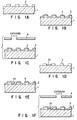
- FIGS. 1A to 1J illustrate sequentially a process of forming a filter pattern according to this invention.
- an aminosilane film (not shown) was deposited on the entire surface of a substrate 1 made of glass.
- a light-absorbing layer 2 of a prescribed pattern and formed of fine particles of graphite was formed over the aminosilane film.
- Blue pigment dispersions each consisting of following composition, were prepared for forming filter patterns of blue, green and red.
- Blue pigment cobalt aluminate ⁇ Cobalt Blue-X (trade name, particle diameter: 0.01 to 0.02 ⁇ m, Toyo Ganryo Co.) ⁇ 30 wt%
- Dispersant ammonium polyacrylate copolymer ⁇ Dispec GA-40 (trade name, Allide Colloid Co.) ⁇ 0.7 wt%
- Adhesion regulating agent fine-grain silica (particle diameter: 0.08 ⁇ m) 3 wt%
- Photoresist ammonium dichromate (ADC) + polyvinyl alcohol (PVA) 0.5 wt% (These component being dispersed in pure water)
- Green pigment dispersion Green pigment: TiO 2 -NiO-CoO-ZnO ⁇ Daipyroxide TM-Green #3320 (trade name, particle diameter: 0.01 to 0.02 ⁇ m, Dain
- the substrate 1 was kept at a temperature of 30°C, and the blue pigment dispersion was coated all over the substrate 1 provided with a light absorbing layer 2 to form a blue pigment layer 3. Subsequently, the substrate 1 was rotated at 100 to 300 rpm to shake off an excessive pigment dispersion. Then, the substrate 1 was heated at a heater temperature of 120°C for 3 to 4 minutes to dry the pigment dispersion. Thereafter, the substrate 1 was subjected to a light exposure of prescribed pattern by using a high pressure mercury lamp with a color-screening electrode 4 being interposed therebetween as shown in FIG. 1C. Then, the substrate 1 was rinsed with a spray of mist-like water for example at a liquid pressure of 2 to 10 kg/cm 2 to obtain a blue pigment pattern 3a of a prescribe pattern as shown in FIG. 1D.
- the substrate 1 was kept at a temperature of 30°C, and the green pigment dispersion was coated all over the substrate 1 to form a green pigment layer 5 as shown in FIG. 1E. Subsequently, the substrate 1 was rotated at 100 to 300 rpm to shake off an excessive pigment dispersion. Then, the substrate 1 was heated at a heater temperature of 120°C for 3 to 4 minutes to dry the pigment dispersion. Thereafter, the substrate 1 was subjected to a light exposure of prescribed pattern by using a high pressure mercury lamp with a color-screening electrode 4 being interposed therebetween as shown in FIG. 1F. Then, the substrate 1 was rinsed with a spray of mist-like water for example at a liquid pressure of 2 to 10 kg/cm 2 to obtain a green pigment pattern 5a of a prescribe pattern as shown in FIG. 1G.
- the substrate 1 was kept at a temperature of 30°C, and the red pigment dispersion was coated all over the substrate 1 to form a red pigment layer 6 as shown in FIG. 1H. Subsequently, the substrate 1 was rotated at 100 to 300 rpm to shake off an excessive pigment dispersion. Then, the substrate 1 was heated at a heater temperature of 120°C for 3 to 4 minutes to dry the pigment dispersion. Then, the substrate 1 was rinsed with a spray of mist-like water for example at a liquid pressure of 2 to 10 kg/cm 2 to obtain a red pigment pattern 6a of a prescribe pattern as shown in FIG. 1I.
- a pigment layer comprising the blue pigment pattern 3a, the green pigment pattern 5a and the red pigment pattern 6a was formed on the substrate 1.
- the substrate since the entire surface of the substrate 1 was covered with an aminosilane film, and at the same time a fine-grain silica was included in the blue pigment pattern 3a, the green pigment pattern 5a and the red pigment pattern 6a, the substrate was charged into a positive charge (+), while the blue pigment pattern 3a, the green pigment pattern 5a and the red pigment pattern 6a were charged into a negative charge (-), respectively.
- the adhesive strength between red pigment pattern 6a and the substrate 1 was made sufficiently larger than the adhesive strength between the red pigment pattern 6a and the blue pigment pattern 3a, or between the red pigment pattern 6a and the green pigment pattern 5a, so that only a portion of the red pigment pattern 6a that was disposed on the blue pigment pattern 3a and on the green pigment pattern 5a was removed.
- the red pigment pattern 6a was formed only on a region of the substrate 1 where any of the blue pigment pattern 3a and on the green pigment pattern 5a was not disposed. Therefore, the process of light-exposure was not required in the formation of the red pigment pattern 6a in contrast to the conventional method requiring the process. Accordingly, the process of forming a color filter was much simplified by the above method.
- a blue fluorescent material layer 7, a green fluorescent material layer 8 and a red fluorescent material layer 9 were formed in conformity with the blue pigment pattern 3a, the green pigment pattern 5a and the red pigment pattern 6a, respectively.
- a filter-attached fluorescent layer having a pigment layer and a fluorescent material layer, each disposed on a substrate 1, was obtained.
- a color picture tube mounting this filter-attached fluorescent layer was confirmed to be excellent in contrast and color purity.
- the filter pattern was formed only on a prescribed portion, i.e. for example a blue pigment pattern was accurately formed on a limited area where a blue fluorescent material layer is to be subsequently formed, a mixture of color was not generated, thus realizing a filter excellent in color purity.
- the first pigment layer is defined as being formed of a blue pigment layer and a green pigment layer
- the second pigment layer is defined as being formed of a red pigment layer.
- this invention is not limited to this combination, but the second pigment layer may be either a blue pigment layer or a green pigment layer. Further, it is possible to apply this invention to the color filter of a liquid crystal display device.
- each pigment layer is patterned, the substrate is immersed in, for example, an alkali developing agent before spraying of mist-like water, thus enabling certainly removal of unnecessary portion of each pigment layer.
- an adhesion regulating agent is added at least either one of a solution containing a first pigment or a solution containing a second pigment, it has become possible to selectively remove only a portion of a second pigment layer which is disposed on a first pigment layer without necessitating the process of light-exposure. Accordingly, a filter pattern can be manufactured in more simplified manner and in high yield by this invention as compared with the conventional method.
Landscapes
- Engineering & Computer Science (AREA)
- Manufacturing & Machinery (AREA)
- Optical Filters (AREA)
- Manufacture Or Reproduction Of Printing Formes (AREA)
Abstract

Description
- This invention relates to a method of manufacturing a display screen, and in particular to a method of manufacturing a display screen provided with a filter pattern.
- The face-plate of color picture tube is provided on its inner surface with a fluorescent material layer of dot or stripe pattern which is capable of emitting red, blue and green light. When an electron beam is impinged upon the fluorescent material layer, the fluorescent material layer emits specific colors thus displaying an image. There have been proposed various improvements of the fluorescent material layer of such a color picture tube in an attempt to improve the quality of display image such as contrast or color purity of the image. For example, there has been proposed a filter-attached fluorescent material layer provided with a pigment layer having the same body colors each corresponding to the emitting colors of the fluorescent material layer, the pigment layer being disposed between a face-plate and the fluorescent material layer. According this filter-attached fluorescent material layer, a red pigment disposed as a filter selectively absorbs green and blue light components from the incident light, likewise a blue pigment selectively absorbs green and red light components, and a green pigment selectively absorbs blue and red light components, so that the quality of display image such as contrast or color purity of the image can be improved.
- As for the method of manufacturing such a filter-attached fluorescent material layer, there is suggested a method as disclosed for example in Japanese Patent Unexamined Publication Hei/5-275008. According to this method, a resist is coated on a substrate, the surface of the resultant resist layer excluding a prescribed portion is exposed to light and then developed thus forming a resist pattern. Then, after a pigment solution is coated over the resist pattern, the resist pattern is removed through an acid hydrolysis together with the portion of the pigment layer coated on the resist pattern, thereby forming a pigment pattern in place. This process is repeated for each color to obtain a pigment pattern of respective color.
- However, since the resist pattern is required to be formed every time each pigment pattern is to be formed according to this conventional method, the number of process is inevitably increased. Therefore, there has been a demand to simplify the manufacture of the filter pattern.
- There has been also proposed another method of forming a pigment pattern as disclosed for example in Japanese Patent Unexamined Publication Hei/5-275007. According to this method, a pigment-dispersed solution comprising a water-soluble polymer such as polyvinyl alcohol (PVA) or polyvinyl pyrrolidone (PVP), and a crosslinking agent such as ammonium dichromate (ADC) or diazonium salt is coated on a substrate to form a pigment layer, which is then subjected to light exposure and developed using a hot water, thereby forming a prescribed pattern of pigment.
- However, since the processes of light exposure and development are required to be repeated every time each color pigment pattern is to be formed in this conventional method, the same problem as mention above is also accompanied in this method.
- Accordingly, an object of the present invention is to provide a method of manufacturing a display screen which makes it possible to form a filter pattern in high yield and in a simplified process.
- Namely, according to the present invention, there is provided a method of manufacturing a display screen provided with a filter pattern comprising a first pigment pattern and a second pigment pattern, which comprises the steps of; forming a first pigment layer by coating a solution containing a first pigment on a surface of a substrate and drying the resultant coated layer; forming a first pigment pattern by subjecting the first pigment layer to a patterned light exposure and developing the resultant exposed pattern; forming a second pigment layer by coating a solution containing a second pigment on the surface of the substrate including a surface of the first pigment pattern; and forming a second pigment pattern by selectively removing, through rinsing, a portion of the second pigment which is disposed on the first pigment pattern; an adhesion regulating agent being contained in at least either one of the solution containing a first pigment and the solution containing a second pigment.
- This invention can be more fully understood from the following detailed description when taken in conjunction with the accompanying drawings, in which:
- FIGS. 1A to 1J illustrate a process of forming a filter pattern according to this invention; and
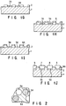
- FIG. 2 is a plan view showing a filter pattern formed by the process shown in FIGS. 1A to 1J.
- This invention provides a method of manufacturing a display screen which makes it possible to form a filter pattern comprising a plurality of pigment patterns of blue, red, green, etc. in high yield and in a reduced number of process. Namely, according to the conventional process of forming a plurality of pigment patterns, the processes of light-exposure and development are required to be repeated for forming each pigment pattern. By contrast, according to this invention, the processes of light-exposure and development are performed only in the formation of the first pigment pattern, and other pigment patterns are subsequently formed, without performing the process of light-exposure, by utilizing a difference in adhesion strength between a substrate and a pigment layer.
- Namely, in a method of manufacturing a display screen according to the present invention, a first pigment layer is formed by coating a solution containing a first pigment on a surface of a substrate and by drying the resultant coated layer. Then, this first pigment layer is subjected to a patterned light exposure and developed forming a first pigment pattern. Then, a second pigment layer is formed by coating a solution containing a second pigment all over the surface of the substrate including a surface of said first pigment pattern and by drying the resultant coated layer. Subsequently, the second pigment layer is rinsed to selectively remove a portion of the second pigment layer which is disposed on the first pigment pattern thereby to form a second pigment pattern. Through these processes, a filter pattern comprising a first pigment pattern and a second pigment pattern can be obtained. In this case, at least either one of the solution containing a first pigment and the solution containing a second pigment is formulated to contain an adhesion regulating agent so as to cause the adhesion strength between the first pigment pattern and the second pigment layer to become lower than the adhesion strength between the substrate and the second pigment layer, thus allowing a portion of the second pigment layer that is formed on the first pigment pattern to be selectively and easily removed.
- This invention will be further explained with a specific example.
- As for the pigment to be useful in this invention, any of inorganic or organic pigments may be employed. In particular, a pigment which is capable of being uniformly dispersed in a filter layer and giving a sufficient transparency to the filter layer without causing scattering of light is preferable.
- Specific examples of such a pigment are as follows.
- With respect to inorganic pigments, a ferric oxide type pigment such as Sicotrans Red L-2817 (trade name, particle diameter: 0.01 to 0.02 µm, BASF Co.) or an anthraquinone type pigment such as Cromophtal Red A2B (trade name, particle diameter: 0.01 µm, Ciba-Geigy Co.) may be used as a red pigment. As for blue pigment, cobalt aluminate type (Al2O3-CoO) pigment such as Cobalt Blue-X (trade name, particle diameter: 0.01 to 0.02 µm, Toyo Ganryo Co.), an ultramarine blue type pigment such as Ultamarine Blue No. 8000 (trade name, particle diameter: 0.01 µm, Dai-ichi Kasei Co.) or a phthalocyanine blue type pigment such as Lionol Blue-FG-7370 (trade name, particle diameter: 0.01 µm, Toyo Ink Co.) may be used. As for green pigment, a TiO2-NiO-CoO-ZnO type pigment such as Daipyroxide TM-Green #3320 (trade name, particle diameter: 0.01 to 0.02 µm, Dainichi Seika Co.), a CoO-Al2O3-Cr2O3-TiO2 type pigment such as Daipyroxide TM-Green #3340 (trade name, particle diameter: 0.01 to 0.02 µm, Dainichi Seika Co.), a CoO-Al2O 3-Cr2O3 type pigment such as Daipyroxide TM-Green #3420 (trade name, particle diameter: 0.01 to 0.02 µm, Dainichi Seika Co.), a Cr2O3 type pigment such as ND-801 (trade name, particle diameter: 0.35 µm, Nihon Denko Co.), a chlorinated phthalocyanine green type pigment such as Fastogen Green S (trade name, particle diameter: 0.01 µm, Dainihon Ink Co.) or a brominated phthalocyanine green type pigment such as Fastogen Green 2YK (trade name, particle diameter: 0.01 µm, Dainihon Ink Co.) may be used.
- With respect to organic pigments, an azolake type pigment such as Lake Red C (trade name, Dainichi Seika Co.) as a red pigment, a copper phthalocyanine type pigment such as Fastogen Blue-GNPS (trade name, Dainihon Ink Co.) as a blue pigment, and a chlorobrominated copper phthalocyanine type pigment such as Lionol Green 2Y-301 (trade name, Toyo Ink Co.) as a green pigment may be used.
- In the manufacture of a pigment dispersion for forming a pigment layer, any of these pigments is mixed together with a dispersant, an adhesion regulating agent, a photoresist and pure water. It is possible to add not more than 5% by weight of a water-soluble organic solvent such as alcohol into pure water.
- Examples of the dispersant for dispersing a pigment are anionic sodium salt dispersant, anionic ammonium salt dispersant and nonionic dispersant. Examples of anionic sodium salt dispersant are acrylic dispersant, acryl-styrene based dispersant, acrylic copolymer, polycarboxylic acid type dispersant and naphthalene sulfonic acid/formalin condensate. Specific examples of such a dispersant are Dispec N-40 (trade name, Allide Colloid Co.) which is an acrylic dispersant, Demol EP (trade name, Kaoh Co.) and Poise 520 (trade name, Kaoh Co.) both of which are a polycarboxylic acid type dispersant, Demol N (trade name, Kaoh Co.) which is a naphthalene sulfonic acid/formalin condensate, Demol MS (trade name, Kaoh Co.) which is a special aromatic sulfonic acid/formalin condensate, and Elenon No.19M (trade name) which is an octylphosphate monoethanol amine salt.
- Examples of anionic ammonium salt dispersant are acrylic dispersant, acryl-styrene based dispersant, acrylic copolymer, polycarboxylic acid type dispersant and polyoxyethylene alkylether sulphate. Specific examples of such a dispersant are Dispec A-40 (trade name, Allide Colloid Co.) which is an acrylic dispersant, Discoat N-14 (trade name, Dai-ichi Kogyo Seiyaku Co.) which is a polycarboxylic acid type dispersant, Hitenol 08 (trade name, Dai-ichi Kogyo Seiyaku Co.) which is an ammonium salt of polyoxyethylene alkylether sulphate, and Lomer PWA (trade name, Sunnovko Co.) which is a naphthalene sulfonic acid condensate.
- Examples of nonionic dispersant are polyoxyethylene laurylether, polyoxyethylene derivatives, polyoxyalkylene alkyl ether, polyoxyethylene nonylphenyl ether, and polyoxyethylene sorbitan monolaurate. Specific examples of such a nonionic dispersant are Noigen EA-140 (trade name, Dai-ichi Kogyo Seiyaku Co.), Emulgen 106 (trade name, Kaoh Co.) and Leodol TW-L120 (trade name, Kaoh Co.).
- Examples of adhesion regulating agent are fine-grain silica, Li-silicate, and fine-grain alumina. With respect to the fine-grain silica and fine-grain alumina, the particle diameter thereof should preferably be 0.1 µm or less.
- As for the photoresist, a water-soluble photoresist such as ammonium dichromate (ADC)/polyvinyl alcohol (PVA), sodium dichromate (SDC)/(PVA), diazonium salt/PVA, stizoval type photoresist or ADC/casein may be used.
- The concentration of the pigment in a pigment dispersion may be 0.1 to 50% by weight, preferably 1 to 50% by weight. If the concentration of the pigment is less than 0.1% by weight, the pigmentation of the pigment layer would become insufficient. If the concentration of the pigment is not less than 1% by weight, the pigmentation of the pigment layer would be clearly recognized. However, if the concentration of the pigment exceeds more than 50% by weight, the viscosity of the dispersion would become too high, thus making it very difficult to form a uniform layer thereof.
- In the followings, the process of forming a pigment pattern and a liquid useful for the developing solution and rinsing solution will be explained. As for the liquid useful for the developing solution and rinsing solution, hot water or an aqueous alkaline solution will be preferably employed.
- The formation of a pigment filter on the panel of a color picture tube may be performed in the following procedure.
- First, a pigment dispersion containing a first pigment is coated on the inner surface of the face plate and then dried. The coating in this case may be performed with the inner surface of the face plate being kept upward, sideways or downward. Parameters such as the solid volume, viscosity and coating method of the pigment dispersion are suitably controlled to obtain a uniform coating of the pigment layer. The coating may be performed using a spin coating method, a dipping method, a flow coating method. The employment of spin coating method may be preferable for obtaining a uniform layer of a prescribed thickness. As for the drying method of the coated layer, a drying with shaking, with heater or with a dry air may be employed. Otherwise, a standing at room temperature for a long period of time may also be employed. As result of drying using any of these methods, a first pigment layer can be obtained.
- It is also possible to form a patterned light-absorbing layer in advance on the inner surface of the face plate before the pigment layer is formed thereon. Then, through a shadow mask of a desired pattern, the pigment layer is exposed to light using for example a high pressure mercury lamp. Thereafter, the inner surface of the face plate is dipped in a developing solution for several seconds to perform the development thereof, thus forming the first pigment pattern.
- Then, a pigment dispersion containing a second pigment is coated on the inner surface of the face plate and then dried, thus forming a second pigment layer. Subsequently, water for example is sprayed on the pigment layer to selectively remove only a portion of the second pigment layer that is deposited on the first pigment pattern, thus forming a second pigment pattern. In this manner, a filter pattern comprising the first and the second pigment patterns can be ultimately obtained.
- According to the method of this invention as described above, it is possible to form a second pigment pattern by merely rinsing the second pigment layer after a solution containing a second pigment is coated all over the surface of the substrate without requiring the process of light exposure. In order to realize this method of this invention, it is very important to make a sufficient degree of difference in adhesivity between the adhesion between the second pigment layer and the substrate, and the adhesion between the second pigment layer and the first pigment layer. After an extensive studies, the present inventors have found the following facts.
- Namely, it has been found that when the substrate is formed of glass, the patterning of the second pigment layer can be easily performed by a simple rinsing treatment if an adhesion regulating agent is added to at least either one of a first pigment layer and a second pigment layer. The effect of the adhesion regulating agent may be considered as follows. When the adhesion regulating agent is added to a pigment layer, the pigment layer can be charged to a prescribed electric charge (for example, fine-grain silica is charged into a negative charge, while Li-silicate and fine-grain alumina are charged into a positive charge). On the other hand, when the surface of the substrate is covered in advance with a silica or aminosilane film before a pigment layer is deposited thereon, the surface of the substrate can be charged to a prescribed electric charge (for example, silica is charged into a negative charge, while aminosilane is charged into a positive charge). Therefore, when the magnitudes of the electric charge of the first and the second pigment layers are controlled respectively to a predetermined value through the action of the adhesion regulating agent, it is possible to make a sufficient degree of difference in adhesivity between the adhesion between the second pigment layer and the substrate, and the adhesion between the second pigment layer and the first pigment layer.
- Namely, when the adhesion strength between the first pigment pattern and the second pigment layer made lower than the adhesion strength between the substrate and the second pigment layer, it is possible to allow a portion of the second pigment layer which has been formed on the first pigment pattern to be selectively and easily removed, thus forming the second pigment pattern.
- This invention will be further explained with reference to the drawings illustrating one embodiment where the first pigment layer is formed of a blue pigment layer and a green pigment layer, while the second pigment layer is formed of a red pigment layer.
- FIGS. 1A to 1J illustrate sequentially a process of forming a filter pattern according to this invention. First, as shown in FIG. 1A, an aminosilane film (not shown) was deposited on the entire surface of a
substrate 1 made of glass. Then, a light-absorbinglayer 2 of a prescribed pattern and formed of fine particles of graphite was formed over the aminosilane film. - Then, the pigment dispersions, each consisting of following composition, were prepared for forming filter patterns of blue, green and red.
(Blue pigment dispersion) Blue pigment: cobalt aluminate {Cobalt Blue-X (trade name, particle diameter: 0.01 to 0.02 µm, Toyo Ganryo Co.)} 30 wt% Dispersant: ammonium polyacrylate copolymer {Dispec GA-40 (trade name, Allide Colloid Co.)} 0.7 wt% Adhesion regulating agent: fine-grain silica (particle diameter: 0.08 µm) 3 wt% Photoresist: ammonium dichromate (ADC) + polyvinyl alcohol (PVA) 0.5 wt% (These component being dispersed in pure water) (Green pigment dispersion) Green pigment: TiO2-NiO-CoO-ZnO {Daipyroxide TM-Green #3320 (trade name, particle diameter: 0.01 to 0.02 µm, Dainichi Seika Co.)} 30 wt% Dispersant: sodium acrylate {Dispec N-40 (trade name, Allide Colloid Co.)} Adhesion regulating agent: fine-grain silica 0.7 wt% (particle diameter: 0.08 µm) 3 wt% Photoresist: ADC + PVA 0.5 wt% (These component being dispersed in pure water) (Red pigment dispersion) Red pigment: fine-grain Fe2O3 (particle diameter: 0.01 to 0.02 µm) 20 wt% Dispersant: ammonium salt of polyoxyethylene alkylether sulphate {Hitenol 08 (trade name, Dai-ichi Kogyo Seiyaku Co.)} 0.7 wt% Adhesion regulating agent: fine-grain silica (particle diameter: 0.08 µm) 3 wt% Photoresist: ADC + PVA 0.5 wt% (These component being dispersed in pure water) - Then, as shown in FIG. 1B, the
substrate 1 was kept at a temperature of 30°C, and the blue pigment dispersion was coated all over thesubstrate 1 provided with a lightabsorbing layer 2 to form ablue pigment layer 3. Subsequently, thesubstrate 1 was rotated at 100 to 300 rpm to shake off an excessive pigment dispersion. Then, thesubstrate 1 was heated at a heater temperature of 120°C for 3 to 4 minutes to dry the pigment dispersion. Thereafter, thesubstrate 1 was subjected to a light exposure of prescribed pattern by using a high pressure mercury lamp with a color-screening electrode 4 being interposed therebetween as shown in FIG. 1C. Then, thesubstrate 1 was rinsed with a spray of mist-like water for example at a liquid pressure of 2 to 10 kg/cm2 to obtain a blue pigment pattern 3a of a prescribe pattern as shown in FIG. 1D. - Then, the
substrate 1 was kept at a temperature of 30°C, and the green pigment dispersion was coated all over thesubstrate 1 to form agreen pigment layer 5 as shown in FIG. 1E. Subsequently, thesubstrate 1 was rotated at 100 to 300 rpm to shake off an excessive pigment dispersion. Then, thesubstrate 1 was heated at a heater temperature of 120°C for 3 to 4 minutes to dry the pigment dispersion. Thereafter, thesubstrate 1 was subjected to a light exposure of prescribed pattern by using a high pressure mercury lamp with a color-screening electrode 4 being interposed therebetween as shown in FIG. 1F. Then, thesubstrate 1 was rinsed with a spray of mist-like water for example at a liquid pressure of 2 to 10 kg/cm2 to obtain a green pigment pattern 5a of a prescribe pattern as shown in FIG. 1G. - Then, the
substrate 1 was kept at a temperature of 30°C, and the red pigment dispersion was coated all over thesubstrate 1 to form ared pigment layer 6 as shown in FIG. 1H. Subsequently, thesubstrate 1 was rotated at 100 to 300 rpm to shake off an excessive pigment dispersion. Then, thesubstrate 1 was heated at a heater temperature of 120°C for 3 to 4 minutes to dry the pigment dispersion. Then, thesubstrate 1 was rinsed with a spray of mist-like water for example at a liquid pressure of 2 to 10 kg/cm2 to obtain a red pigment pattern 6a of a prescribe pattern as shown in FIG. 1I. - As a result, a pigment layer comprising the blue pigment pattern 3a, the green pigment pattern 5a and the red pigment pattern 6a was formed on the
substrate 1. - In the example explained above, since the entire surface of the
substrate 1 was covered with an aminosilane film, and at the same time a fine-grain silica was included in the blue pigment pattern 3a, the green pigment pattern 5a and the red pigment pattern 6a, the substrate was charged into a positive charge (+), while the blue pigment pattern 3a, the green pigment pattern 5a and the red pigment pattern 6a were charged into a negative charge (-), respectively. As a result, the adhesive strength between red pigment pattern 6a and thesubstrate 1 was made sufficiently larger than the adhesive strength between the red pigment pattern 6a and the blue pigment pattern 3a, or between the red pigment pattern 6a and the green pigment pattern 5a, so that only a portion of the red pigment pattern 6a that was disposed on the blue pigment pattern 3a and on the green pigment pattern 5a was removed. Namely, the red pigment pattern 6a was formed only on a region of thesubstrate 1 where any of the blue pigment pattern 3a and on the green pigment pattern 5a was not disposed. Therefore, the process of light-exposure was not required in the formation of the red pigment pattern 6a in contrast to the conventional method requiring the process. Accordingly, the process of forming a color filter was much simplified by the above method. - Then, according to the conventional method, a blue
fluorescent material layer 7, a greenfluorescent material layer 8 and a redfluorescent material layer 9 were formed in conformity with the blue pigment pattern 3a, the green pigment pattern 5a and the red pigment pattern 6a, respectively. - With these processes, a filter-attached fluorescent layer having a pigment layer and a fluorescent material layer, each disposed on a
substrate 1, was obtained. A color picture tube mounting this filter-attached fluorescent layer was confirmed to be excellent in contrast and color purity. Moreover, since the filter pattern was formed only on a prescribed portion, i.e. for example a blue pigment pattern was accurately formed on a limited area where a blue fluorescent material layer is to be subsequently formed, a mixture of color was not generated, thus realizing a filter excellent in color purity. - The following features can be noted as other embodiments of this invention.
- (a) When a film consisting of aminosilane is formed on the substrate.
An adhesion regulating agent is not added to a blue pigment dispersion as well as to a green pigment dispersion, but added only to a red pigment dispersion. - (b) When a film consisting of silica is formed on the substrate.
- 1. Li-silicate or fine-grain alumina is added to all of a blue pigment dispersion, a green pigment dispersion and a red pigment dispersion.
- 2. An adhesion regulating agent is not added to a blue pigment dispersion as well as to a green pigment dispersion, but Li-silicate or fine-grain alumina is added only to a red pigment dispersion.
- In the above example, the first pigment layer is defined as being formed of a blue pigment layer and a green pigment layer, while the second pigment layer is defined as being formed of a red pigment layer. However, this invention is not limited to this combination, but the second pigment layer may be either a blue pigment layer or a green pigment layer. Further, it is possible to apply this invention to the color filter of a liquid crystal display device.
- Further, where each pigment layer is patterned, the substrate is immersed in, for example, an alkali developing agent before spraying of mist-like water, thus enabling certainly removal of unnecessary portion of each pigment layer.
- As explained above, since an adhesion regulating agent is added at least either one of a solution containing a first pigment or a solution containing a second pigment, it has become possible to selectively remove only a portion of a second pigment layer which is disposed on a first pigment layer without necessitating the process of light-exposure. Accordingly, a filter pattern can be manufactured in more simplified manner and in high yield by this invention as compared with the conventional method.
Claims (14)
- A method of manufacturing a display screen provided with a filter pattern comprising a first pigment pattern and a second pigment pattern, which comprises the steps of;
forming a first pigment layer (3, 5) by coating a solution containing a first pigment on a surface of a substrate (1) and drying the resultant coated layer;
forming a first pigment pattern (3a, 5a) by subjecting said first pigment layer (3, 5) to a patterned light exposure and developing the resultant exposed pattern;
forming a second pigment layer (6) by coating a solution containing a second pigment on the surface of the substrate including a surface of said first pigment pattern (3a, 5a); and
forming a second pigment pattern (6a) by patterning said second pigment layer (6),
characterized in that the patterning of said second pigment layer (6) is carried out by selectively removing, through rinsing, a portion of said second pigment layer (6) which is disposed on said first pigment pattern (3a, 5a), and an adhesion regulating agent is contained in at least either one of said solution containing a first pigment and said solution containing a second pigment. - The method according to claim 1, characterized in that said substrate (1) has a film consisting essentially of silica or aminosilane formed thereon.
- The method according to claim 1, characterized in that said adhesion regulating agent is selected from the group consisting of fine-grain silica, Li-silica and fine-grain alumina.
- The method according to claim 1, characterized in that each of said fine-grain silica and fine-grain alumina has a particle diameter of 0.1 µm or less.
- The method according to claim 1, characterized in that said adhesion regulating agent is included in the solution at a ratio of 10 to 60% by weight.
- The method according to claim 1, characterized in that said solution containing a first pigment contains a photosensitive resin.
- The method according to claim 1, characterized by further comprising a step of forming a light-absorbing pattern on the substrate (1) before the first pigment layer (3, 5) is formed.
- The method according to claim 1, characterized in that each of said solution containing a first pigment and said solution containing a second pigment contains a dispersant.
- The method according to claim 1, characterized in that a film consisting essentially of aminosilane is formed on an entire surface of the substrate (1), an adhesion regulating agent is not added to said solution containing a first pigment, but fine-grain silica is added to said solution containing a second pigment.
- The method according to claim 1, characterized in that a film consisting essentially of silica is formed on the substrate (1), and Li-silicate or fine-grain alumina is added to said solution containing a first pigment and to said solution containing a second pigment.
- The method according to claim 1, characterized in that a film consisting essentially of silica is formed on an entire surface of the substrate, and an adhesion regulating agent is not added to said solution containing a first pigment, and Li-silicate or fine-grain alumina is added to said solution containing a second pigment.
- The method according to claim 1, characterized in that each of said solution containing a first pigment and said solution containing a second pigment contains the pigment at a ratio of 0.1 to 50% by weight.
- The method according to claim 1, characterized in that each of said solution containing a first pigment and said solution containing a second pigment contains the pigment at a ratio of 1 to 50% by weight.
- The method according to claim 1, characterized by further comprises a step of forming, after the formation of said second pigment pattern, a first and a second fluorescent material patterns on said first pigment pattern and said second pigment pattern.
Applications Claiming Priority (3)
| Application Number | Priority Date | Filing Date | Title |
|---|---|---|---|
| JP322065/94 | 1994-12-26 | ||
| JP32206594 | 1994-12-26 | ||
| JP32206594 | 1994-12-26 |
Publications (3)
| Publication Number | Publication Date |
|---|---|
| EP0720204A2 true EP0720204A2 (en) | 1996-07-03 |
| EP0720204A3 EP0720204A3 (en) | 1997-08-13 |
| EP0720204B1 EP0720204B1 (en) | 2000-09-06 |
Family
ID=18139530
Family Applications (1)
| Application Number | Title | Priority Date | Filing Date |
|---|---|---|---|
| EP95120049A Expired - Lifetime EP0720204B1 (en) | 1994-12-26 | 1995-12-19 | Method of manufacturing display screen |
Country Status (7)
| Country | Link |
|---|---|
| US (1) | US5700609A (en) |
| EP (1) | EP0720204B1 (en) |
| KR (1) | KR100219903B1 (en) |
| CN (1) | CN1061776C (en) |
| DE (1) | DE69518731T2 (en) |
| MY (1) | MY113219A (en) |
| TW (1) | TW297133B (en) |
Cited By (3)
| Publication number | Priority date | Publication date | Assignee | Title |
|---|---|---|---|---|
| EP0865066A2 (en) * | 1997-03-11 | 1998-09-16 | Kabushiki Kaisha Toshiba | Method of manufacturing screen of color picture tube |
| CN1100337C (en) * | 1996-08-15 | 2003-01-29 | 东芝株式会社 | Method for forming fluorescent surface |
| WO2003023816A2 (en) * | 2001-09-13 | 2003-03-20 | Koninklijke Philips Electronics N.V. | Electric lamp, lamp vessel provided with a light-absorbing coating and method of preparing such a licht-absorbing coating |
Families Citing this family (7)
| Publication number | Priority date | Publication date | Assignee | Title |
|---|---|---|---|---|
| MY118433A (en) * | 1994-12-26 | 2004-11-30 | Toshiba Kk | Display screen, method of manufacturing the same, and cathode ray tube |
| CN101187710A (en) * | 1996-01-11 | 2008-05-28 | 株式会社东芝 | Method for forming color filtering film pattern on non-fibrous substrate and formed color filter film |
| WO1998018147A1 (en) * | 1996-10-17 | 1998-04-30 | Philips Electronics N.V. | Method of manufacturing a color display device comprising color-filter layers |
| KR19990072174A (en) * | 1996-10-17 | 1999-09-27 | 요트.게.아. 롤페즈 | Color display device with color-filter layers |
| KR19990072175A (en) * | 1996-10-17 | 1999-09-27 | 요트.게.아. 롤페즈 | Color display device with color-filter layers |
| KR100467676B1 (en) * | 1998-11-20 | 2005-06-08 | 삼성에스디아이 주식회사 | Cathode ray tube color filter dispersion and color filter formation method using the same |
| KR101222947B1 (en) | 2005-06-30 | 2013-01-17 | 엘지디스플레이 주식회사 | Solvent for printing, pattern composition for printing, and pattering method using the same |
Citations (3)
| Publication number | Priority date | Publication date | Assignee | Title |
|---|---|---|---|---|
| FR2225836A1 (en) * | 1973-04-16 | 1974-11-08 | Hitachi Ltd | |
| US5340673A (en) * | 1992-03-25 | 1994-08-23 | Sony Corporation | Method of manufacturing a phosphor screen of a cathode ray tube |
| EP0647690A2 (en) * | 1993-10-08 | 1995-04-12 | Kabushiki Kaisha Toshiba | Pigment dispersion composition, display apparatus, and method of manufacturing the apparatus |
Family Cites Families (4)
| Publication number | Priority date | Publication date | Assignee | Title |
|---|---|---|---|---|
| GB834030A (en) * | 1955-09-06 | 1960-05-04 | Sam H Kaplan | Improvements in electron discharge devices used for picture reproduction in colour television systems and methods of manufacturing such devices |
| US2959483A (en) * | 1955-09-06 | 1960-11-08 | Zenith Radio Corp | Color image reproducer and method of manufacture |
| US3891440A (en) * | 1973-11-02 | 1975-06-24 | Gte Sylvania Inc | Process for fabricating a color cathode ray tube screen structure incorporating optical filter means therein |
| JP3297929B2 (en) * | 1992-03-25 | 2002-07-02 | ソニー株式会社 | Method for forming fluorescent screen of cathode ray tube |
-
1995
- 1995-12-19 DE DE69518731T patent/DE69518731T2/en not_active Expired - Fee Related
- 1995-12-19 EP EP95120049A patent/EP0720204B1/en not_active Expired - Lifetime
- 1995-12-19 TW TW084113587A patent/TW297133B/zh active
- 1995-12-21 MY MYPI95004006A patent/MY113219A/en unknown
- 1995-12-22 US US08/577,095 patent/US5700609A/en not_active Expired - Fee Related
- 1995-12-26 KR KR1019950072354A patent/KR100219903B1/en not_active IP Right Cessation
- 1995-12-26 CN CN95113144A patent/CN1061776C/en not_active Expired - Fee Related
Patent Citations (3)
| Publication number | Priority date | Publication date | Assignee | Title |
|---|---|---|---|---|
| FR2225836A1 (en) * | 1973-04-16 | 1974-11-08 | Hitachi Ltd | |
| US5340673A (en) * | 1992-03-25 | 1994-08-23 | Sony Corporation | Method of manufacturing a phosphor screen of a cathode ray tube |
| EP0647690A2 (en) * | 1993-10-08 | 1995-04-12 | Kabushiki Kaisha Toshiba | Pigment dispersion composition, display apparatus, and method of manufacturing the apparatus |
Cited By (6)
| Publication number | Priority date | Publication date | Assignee | Title |
|---|---|---|---|---|
| CN1100337C (en) * | 1996-08-15 | 2003-01-29 | 东芝株式会社 | Method for forming fluorescent surface |
| EP0865066A2 (en) * | 1997-03-11 | 1998-09-16 | Kabushiki Kaisha Toshiba | Method of manufacturing screen of color picture tube |
| EP0865066A3 (en) * | 1997-03-11 | 1999-04-14 | Kabushiki Kaisha Toshiba | Method of manufacturing screen of color picture tube |
| WO2003023816A2 (en) * | 2001-09-13 | 2003-03-20 | Koninklijke Philips Electronics N.V. | Electric lamp, lamp vessel provided with a light-absorbing coating and method of preparing such a licht-absorbing coating |
| WO2003023816A3 (en) * | 2001-09-13 | 2003-06-05 | Koninkl Philips Electronics Nv | Electric lamp, lamp vessel provided with a light-absorbing coating and method of preparing such a licht-absorbing coating |
| US7740900B2 (en) | 2001-09-13 | 2010-06-22 | Koninklijke Philips Electronics N.V. | Method of preparing a light-absorbing coating |
Also Published As
| Publication number | Publication date |
|---|---|
| CN1061776C (en) | 2001-02-07 |
| DE69518731D1 (en) | 2000-10-12 |
| DE69518731T2 (en) | 2004-07-01 |
| TW297133B (en) | 1997-02-01 |
| KR100219903B1 (en) | 1999-09-01 |
| CN1130298A (en) | 1996-09-04 |
| EP0720204B1 (en) | 2000-09-06 |
| US5700609A (en) | 1997-12-23 |
| EP0720204A3 (en) | 1997-08-13 |
| MY113219A (en) | 2001-12-31 |
Similar Documents
| Publication | Publication Date | Title |
|---|---|---|
| EP0647690B1 (en) | Pigment dispersion composition, display apparatus, and method of manufacturing the apparatus | |
| EP0720204B1 (en) | Method of manufacturing display screen | |
| EP0720200B1 (en) | Display screen, method of manufacturing the same, and cathode ray tube | |
| JP3648331B2 (en) | Method for forming fluorescent screen with filter of color cathode ray tube | |
| JP3853853B2 (en) | Filter pattern manufacturing method | |
| KR20000022422A (en) | Photosensitive composition and method of pattern formation | |
| JP3558764B2 (en) | Filter pattern and manufacturing method thereof | |
| JP3853852B2 (en) | Method for producing phosphor layer with filter | |
| JPH08236020A (en) | Manufacture of filter pattern | |
| JPH07179711A (en) | Pigment dispersion composition, display having fluorescent membrane equipped with a filter and its production | |
| EP0865066B1 (en) | Method of manufacturing screen of color picture tube | |
| JPH09222509A (en) | Production of filter pattern | |
| JPH08185799A (en) | Manufacture of color cathode-ray tube | |
| KR100266035B1 (en) | A manufacturing method of phosphor layer for a color cathode ray tube | |
| JPH11233018A (en) | Forming method for fluorescent screen with filter for color cathode-ray tube | |
| JP3637161B2 (en) | Color cathode ray tube | |
| KR100199386B1 (en) | Method of manufacturing display screen | |
| JPH11354026A (en) | Color filter forming method | |
| JPH11339682A (en) | Color cathode-ray tube | |
| JP2000223019A (en) | Forming method for color filter | |
| JP2000039511A (en) | Formation of color filter | |
| KR20010002253A (en) | Method manufacturing phosphor layer of color image display device | |
| JPH08180809A (en) | Development of phosphor screen of color picture tube | |
| JPH10233162A (en) | Developing method for fluorescent screen of color picture tube | |
| JPH06265718A (en) | Production of color filter |
Legal Events
| Date | Code | Title | Description |
|---|---|---|---|
| PUAI | Public reference made under article 153(3) epc to a published international application that has entered the european phase |
Free format text: ORIGINAL CODE: 0009012 |
|
| 17P | Request for examination filed |
Effective date: 19960116 |
|
| AK | Designated contracting states |
Kind code of ref document: A2 Designated state(s): DE FR GB |
|
| PUAL | Search report despatched |
Free format text: ORIGINAL CODE: 0009013 |
|
| AK | Designated contracting states |
Kind code of ref document: A3 Designated state(s): DE FR GB |
|
| GRAG | Despatch of communication of intention to grant |
Free format text: ORIGINAL CODE: EPIDOS AGRA |
|
| 17Q | First examination report despatched |
Effective date: 19990730 |
|
| GRAG | Despatch of communication of intention to grant |
Free format text: ORIGINAL CODE: EPIDOS AGRA |
|
| GRAH | Despatch of communication of intention to grant a patent |
Free format text: ORIGINAL CODE: EPIDOS IGRA |
|
| GRAH | Despatch of communication of intention to grant a patent |
Free format text: ORIGINAL CODE: EPIDOS IGRA |
|
| GRAH | Despatch of communication of intention to grant a patent |
Free format text: ORIGINAL CODE: EPIDOS IGRA |
|
| GRAA | (expected) grant |
Free format text: ORIGINAL CODE: 0009210 |
|
| AK | Designated contracting states |
Kind code of ref document: B1 Designated state(s): DE FR GB |
|
| REF | Corresponds to: |
Ref document number: 69518731 Country of ref document: DE Date of ref document: 20001012 |
|
| ET | Fr: translation filed | ||
| PLBE | No opposition filed within time limit |
Free format text: ORIGINAL CODE: 0009261 |
|
| STAA | Information on the status of an ep patent application or granted ep patent |
Free format text: STATUS: NO OPPOSITION FILED WITHIN TIME LIMIT |
|
| 26N | No opposition filed | ||
| REG | Reference to a national code |
Ref country code: GB Ref legal event code: IF02 |
|
| PGFP | Annual fee paid to national office [announced via postgrant information from national office to epo] |
Ref country code: FR Payment date: 20061208 Year of fee payment: 12 |
|
| PGFP | Annual fee paid to national office [announced via postgrant information from national office to epo] |
Ref country code: GB Payment date: 20061213 Year of fee payment: 12 |
|
| PGFP | Annual fee paid to national office [announced via postgrant information from national office to epo] |
Ref country code: DE Payment date: 20061214 Year of fee payment: 12 |
|
| GBPC | Gb: european patent ceased through non-payment of renewal fee |
Effective date: 20071219 |
|
| PG25 | Lapsed in a contracting state [announced via postgrant information from national office to epo] |
Ref country code: DE Free format text: LAPSE BECAUSE OF NON-PAYMENT OF DUE FEES Effective date: 20080701 |
|
| REG | Reference to a national code |
Ref country code: FR Ref legal event code: ST Effective date: 20081020 |
|
| PG25 | Lapsed in a contracting state [announced via postgrant information from national office to epo] |
Ref country code: GB Free format text: LAPSE BECAUSE OF NON-PAYMENT OF DUE FEES Effective date: 20071219 |
|
| PG25 | Lapsed in a contracting state [announced via postgrant information from national office to epo] |
Ref country code: FR Free format text: LAPSE BECAUSE OF NON-PAYMENT OF DUE FEES Effective date: 20071231 |