EP0718983A1 - Spreizspektrumdifferenzmodulation - Google Patents
Spreizspektrumdifferenzmodulation Download PDFInfo
- Publication number
- EP0718983A1 EP0718983A1 EP95402818A EP95402818A EP0718983A1 EP 0718983 A1 EP0718983 A1 EP 0718983A1 EP 95402818 A EP95402818 A EP 95402818A EP 95402818 A EP95402818 A EP 95402818A EP 0718983 A1 EP0718983 A1 EP 0718983A1
- Authority
- EP
- European Patent Office
- Prior art keywords
- signal
- pseudo
- sequence
- symbols
- sequences
- Prior art date
- Legal status (The legal status is an assumption and is not a legal conclusion. Google has not performed a legal analysis and makes no representation as to the accuracy of the status listed.)
- Granted
Links
- 238000001228 spectrum Methods 0.000 title claims abstract description 43
- 238000000034 method Methods 0.000 claims abstract description 44
- 230000003111 delayed effect Effects 0.000 claims abstract description 13
- 230000005540 biological transmission Effects 0.000 claims description 32
- 230000004044 response Effects 0.000 claims description 14
- 238000001914 filtration Methods 0.000 claims description 11
- 230000010354 integration Effects 0.000 claims description 6
- 230000000875 corresponding effect Effects 0.000 description 11
- 238000010586 diagram Methods 0.000 description 10
- 238000005311 autocorrelation function Methods 0.000 description 5
- 230000001427 coherent effect Effects 0.000 description 5
- 230000010363 phase shift Effects 0.000 description 5
- 230000007480 spreading Effects 0.000 description 5
- 230000008901 benefit Effects 0.000 description 4
- 230000008569 process Effects 0.000 description 4
- 230000000295 complement effect Effects 0.000 description 3
- 238000007796 conventional method Methods 0.000 description 3
- 238000005314 correlation function Methods 0.000 description 3
- 244000045947 parasite Species 0.000 description 3
- 230000000694 effects Effects 0.000 description 2
- 238000005562 fading Methods 0.000 description 2
- 230000006872 improvement Effects 0.000 description 2
- 238000004519 manufacturing process Methods 0.000 description 2
- 230000003071 parasitic effect Effects 0.000 description 2
- 230000009467 reduction Effects 0.000 description 2
- 239000000758 substrate Substances 0.000 description 2
- 238000010897 surface acoustic wave method Methods 0.000 description 2
- 230000007704 transition Effects 0.000 description 2
- 241001644893 Entandrophragma utile Species 0.000 description 1
- 235000001855 Portulaca oleracea Nutrition 0.000 description 1
- 244000234609 Portulaca oleracea Species 0.000 description 1
- 239000000654 additive Substances 0.000 description 1
- 230000000996 additive effect Effects 0.000 description 1
- XAGFODPZIPBFFR-UHFFFAOYSA-N aluminium Chemical compound [Al] XAGFODPZIPBFFR-UHFFFAOYSA-N 0.000 description 1
- 229910052782 aluminium Inorganic materials 0.000 description 1
- 230000015572 biosynthetic process Effects 0.000 description 1
- 230000002596 correlated effect Effects 0.000 description 1
- 230000007547 defect Effects 0.000 description 1
- 230000001934 delay Effects 0.000 description 1
- 230000001747 exhibiting effect Effects 0.000 description 1
- 239000000284 extract Substances 0.000 description 1
- PCHJSUWPFVWCPO-UHFFFAOYSA-N gold Chemical compound [Au] PCHJSUWPFVWCPO-UHFFFAOYSA-N 0.000 description 1
- 239000010931 gold Substances 0.000 description 1
- 229910052737 gold Inorganic materials 0.000 description 1
- 238000012545 processing Methods 0.000 description 1
- 239000010453 quartz Substances 0.000 description 1
- 238000012552 review Methods 0.000 description 1
- 230000000630 rising effect Effects 0.000 description 1
- VYPSYNLAJGMNEJ-UHFFFAOYSA-N silicon dioxide Inorganic materials O=[Si]=O VYPSYNLAJGMNEJ-UHFFFAOYSA-N 0.000 description 1
- 230000003595 spectral effect Effects 0.000 description 1
- 230000001131 transforming effect Effects 0.000 description 1
Images


Classifications
-
- H—ELECTRICITY
- H04—ELECTRIC COMMUNICATION TECHNIQUE
- H04J—MULTIPLEX COMMUNICATION
- H04J13/00—Code division multiplex systems
- H04J13/16—Code allocation
- H04J13/18—Allocation of orthogonal codes
-
- H—ELECTRICITY
- H04—ELECTRIC COMMUNICATION TECHNIQUE
- H04B—TRANSMISSION
- H04B1/00—Details of transmission systems, not covered by a single one of groups H04B3/00 - H04B13/00; Details of transmission systems not characterised by the medium used for transmission
- H04B1/69—Spread spectrum techniques
- H04B1/707—Spread spectrum techniques using direct sequence modulation
-
- H—ELECTRICITY
- H04—ELECTRIC COMMUNICATION TECHNIQUE
- H04J—MULTIPLEX COMMUNICATION
- H04J13/00—Code division multiplex systems
- H04J13/0007—Code type
- H04J13/0022—PN, e.g. Kronecker
Definitions
- the subject of the present invention is a transmission method with differential modulation and demodulation of spread spectrum phase using orthogonal pseudo-random sequences.
- the direct sequence spread spectrum modulation technique has been used for many years, in particular in radiocommunications with satellites and in the military field.
- a radio carrier is modulated by phase, or frequency, or amplitude or mixed modulation.
- phase modulations which are the most used today.
- the digital data to be transmitted are binary elements, or bits. These bits have a period T b , that is to say that every T b must transmit a new bit. With these bits, symbols can be formed whose period is denoted T s . These are the symbols that will modulate the radio carrier. The symbol rate is expressed in bauds (or symbols / seconds).
- coherent demodulation On the reception side, there are two main families of demodulation: coherent demodulation and non-coherent demodulation.
- the coherent demodulation techniques consist in producing, in the receiver, a subset whose role is to estimate the mean phase of the carrier, so as to reconstitute a phase reference. This phase reference is then mixed with the received signal to demodulate the data.
- This technique is the most effective in radio channels where Gaussian noise is added to the useful signal. This is the case, for example, for transmissions with satellites. However, in the presence of multiple paths, this technique gives very poor results.
- the non-coherent demodulation technique is based on the observation that it is sufficient that the phase reference of the current symbol is the phase of the previous symbol. In this case, the receiver does not estimate the phase of the symbols but the phase difference between two successive symbols. We are then in the presence of differential phase modulation DPSK ("Differential Phase Shift Keying") or DQPSK ("Differential Quadrature Phase Shit Keying").
- DPSK Different Phase Shift Keying
- DQPSK Differential Quadrature Phase Shit Keying
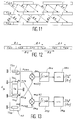
- FIG. 1 attached shows the block diagram of a DPSK transmitter.
- This transmitter has an input Ee, which receives the data b k to be transmitted, which have a period T b , and it comprises a differential encoder 10 composed of a logic circuit 12 and a delay circuit 14, a local oscillator 16 delivering a carrier P and a modulator 18 connected to an output Se which delivers the DPSK signal.
- the logic circuit 12 receives the binary data b k and delivers other binary data called symbols and denoted d k .
- the logic circuit 12 also receives the symbols delayed by a period T b , ie d k-1 .
- the modulator 18 modulates the carrier P in phase as a function of each symbol d k .
- FIG. 2 attached shows the block diagram of a corresponding receiver, of the demodulator type differential.
- This receiver has an input Er and comprises a bandpass filter 20, a delay circuit 22 of duration Tb, a multiplier 24, an integrator 26 which operates over a period Tb and a logic decision circuit 28.
- the receiver has an output Sr which restores the data b k .
- the passband of the input filter 20 is between the NYQUIST band (equal to 1 / T b ) and the width of the main lobe of the DPSK signal, (which is 2 / T b ).
- the multiplier 24 receives a filtered signal x F (t) coming directly from the filter 20 and a filtered-delayed signal x FR coming from the delay circuit 22 It delivers a product signal denoted m (t) which is integrated over a period T b into the integrator 26.
- the latter delivers a signal whose polarity makes it possible to determine the value of the bit transmitted, which logic 28 decides.
- the direct sequence spread spectrum technique consists in multiplying the sequence of symbols d k obtained after the differential coding by a pseudo-random sequence having a bit rate much higher than the bit rate of the data to be transmitted.
- This pseudo-random sequence has a bit rate N times higher than the bit rate of the binary data to be transmitted.
- the duration T c of a binary element of this pseudo-random sequence, an element also called "chip" is therefore equal to T b / N.
- the chip rate of the pseudo-random sequence can be several megachips, or even several tens of megachips per second.
- Figure 3 shows the block diagram of a direct sequence spread spectrum transmitter.
- the elements already shown in Figure 1 have the same references.
- the transmitter comprises, in addition to that of FIG. 1, a generator 30 of pseudo-random sequence (C) and a multiplier 32.
- the signal delivered by the multiplier has a spectrum spread by the pseudo-random sequence.
- the modulator 18 then no longer works on the original symbol d k but on the corresponding spread symbol D k .
- the corresponding receiver has the same structure as the receiver of FIG. 2, except that the filter 20 is now a suitable filter whose impulse response brought back into baseband is the conjugate complex reversed in time of the pseudo-random sequence used in the transmitter.
- the pseudo-random sequence used on transmission must have an autocorrelation function exhibiting a marked peak (of value N) for zero delay and the lowest possible side lobes. This can be obtained by using maximum length sequences (also called m-sequences) or so-called GOLD or KASAMI sequences for example.
- the adapted filter therefore achieves the correlation between the signal applied to its input and the pseudo-random spreading sequence.
- the signal x F (t) will therefore be in the form of a pulse signal whose repetition frequency is equal to 1 / T b .
- the envelope of this signal is the autocorrelation function of the signal C (t).
- the information is conveyed by the phase difference between two successive correlation peaks.
- the output of the multiplier will therefore be formed of a succession of positive or negative peaks, depending on the value of the transmitted bit.
- the output of the matched filter will be formed of a succession of correlation peaks, each peak corresponding to a propagation path.
- Line (a) represents the filtered signal x F (t); line (b) the correlation signal x F (t) * x F (T s -t); line (c) the signal at the output of the integrator.
- each correlation peak at the output of the matched filter may take four phase states, whereas there were only two with DPSK modulation.
- X FR (t) d -2 VS VS E , VS R (-t) + d -1 VS VS E ,VS R (T b - t).
- the object of the present invention is precisely to remedy this drawback and aims to improve the quality of the output signal from the demodulator (signal m (t)) and, in doing so, the quality of the transmission.
- the invention proposes a new method of transmission by differential spread spectrum modulation and demodulation in which, essentially, two pseudo-random sequences on transmission are used, orthogonal to one another, these two sequences used to spread the spectrum of symbols, which will then modulate a carrier.
- two filterings will be carried out adapted to these two orthogonal sequences.
- the filtered-delayed signal associated with one of the sequences will be multiplied by the filtered (but not delayed) signal associated with the other sequence.
- the parasites affecting these signals will be decorrelated which will decrease their influence on the demodulation signal.
- the two filtered-delayed and filtered signals respectively emanated from the same filter, so that the parasites affecting them were correlated.
- the subject of the present invention is a method for transmitting data by differential spread spectrum modulation and demodulation in which, the data being organized into at least one series of binary data having a certain period, characterized in that:
- the invention presents several embodiments depending on whether one transmits a single data stream, or two, or more than two.
- FIG. 5 shows a diagram of a particular embodiment of a transmitter according to the invention.
- This transmitter comprises means already shown in FIG. 3 and which bear the same references, namely an input Ee receiving the binary data b k to be transmitted, these data having a period T b , a differential encoder 10 with its logic circuit 12 and its delay circuit 14.
- This coder delivers symbols d k .
- the transmitter shown includes in addition, a first generator 30 1 delivering a first pseudo-random sequence C E1 applied to a first multiplier 32 1 and a second generator 30 2 delivering a second pseudo-random sequence C E2 applied to a second multiplier 32 2 .
- Multipliers 32 1 and 32 2 deliver symbols (D k ) 1 and (D k ) 2 whose spectrum is spread by the corresponding sequences.
- the transmitter further comprises a first modulator 18 1 receiving a carrier P produced by a local oscillator 16 and the symbols (D k ) 1 spread by the first pseudo-random sequence C E1 and a second modulator 18 2 receiving this same carrier P and the symbols (D k ) 2 spread by the second pseudo-random sequence C E2 .
- an adder 31 is connected to the two modulators 18 1 and 18 2 and supplies the output Se of the transmitter. This output emits the carrier modulated by the doubly spread signal.
- the modulation can be arbitrary (phase, frequency, mixed, etc.).
- this circuit could be modified by first adding the two spread signals (D k ) 1 and (D k ) 2 and using a single modulator. We could also add the two pseudo-random sequences C E1 and C E2 as soon as they are formed and spread the signal using the pseudo-random sum obtained.
- the receiver shown in Figure 6 includes means already shown in Figure 2, namely an input Er receiving a signal x (t), a delay circuit 22 of duration equal to the period T b of the transmitted bits, a multiplier 24 , delivering a demodulation signal m (t), an integration circuit 26 acting on the signal m (t) delivered by the multiplier 24, the integration taking place between 0 and T b , a decision logic circuit 28 and a general output Sr finally delivering the digital data b k of origin.
- This receiver differs from the prior art in that it comprises a first filter 20 1 adapted to the first pseudo-random sequence C E1 used in the transmitter and a second filter 20 2 adapted to the second pseudo-random sequence C E2 used in the 'transmitter.
- filter adapted to a pseudo-random sequence is also understood a filter whose impulse response brought back into baseband is the conjugate complex reversed in time of the pseudo-random sequence in question.
- the first filter 20 1 delivers a filtered signal x F1 which is then delayed by T b in a circuit 22 to give a filtered-delayed signal x FR1 .
- the second filter 20 2 delivers a filtered signal x F2 . This signal is not delayed and is used to produce the demodulation signal m (t) by multiplication with the filtered-delayed signal X FR1 .
- the binary quantities which will be used to modulate the carrier are the symbols d k obtained from the original data b k after passing through the differential encoder 10.
- the symbols d k are multiplied by a single pseudo-random sequence C E.
- the symbols d k are multiplied by the two pseudo-random sequences C E1 and C E2 , orthogonal to each other, to form a signal which will modulate the carrier.
- the filtered-delayed signal x FR1 at the output of the delay circuit 22 can be written:
- the filtered signal x F2 at the output of the filter 20 2 can be written:
- the two signals received by the demodulator 24 are different both by their rank and by the pseudo-random sequence which they imply: the signal x FR1 has been delayed by a duration T b and therefore corresponds, on transmission, to a symbol of rank k-1, while the signal x F2 corresponds to the following symbol of rank k; moreover, the signal x FR1 comes from a symbol which has been spread and then despread by the first sequence C E1 , while the signal x F2 has been processed by the second sequence C E2 . Due to the delay in rank between the symbols in question, it can be seen that the sequences C E1 and C E2 were not transmitted at the same time on transmission.
- Each sequence is indeed transmitted periodically with the same period T b as the symbols to be processed, but the sequence C E1 linked to the signal x FR1 was transmitted one row before the sequence C E2 linked to the signal x F2 .
- the two sequences C E1 and C E2 although generally produced simultaneously by the generators 30 1 and 30 2 , in fact intervene in a shifted manner by a row, and this because of the processing carried out upon reception of the sequences.
- a C E1 sequence is therefore always used first and then a C E2 sequence.
- Figure 7 shows this process schematically.
- the first sequence C E1 is repeated periodically at each symbol d k-1 , d k , d k + 1 , etc., as is the second sequence C E2 .
- These sequences are symbolized by the rectangles of the upper and lower bands respectively.
- the demodulation signal m (t) is formed from a signal x FR1 which has its origin from a symbol of rank k-1 processed by C E1 and a signal x F1 which has its origin of a rank symbol k processed by C E2 .
- the downward oblique arrow going from a sequence C E1 of rank k-1 to a sequence C E2 of rank k symbolizes the chronology of the sequences used. This chronology is repeated with each formation of a new demodulation signal. All the downward oblique arrows symbolize the transmission of all the symbols d k when k increases from unit to unit.
- FIG. 9 shows how to modify the diagrams of the transmitter and receiver compared to Figures 5 and 6 to implement this double transmission.
- the transmitter of FIG. 9 presents two inputs Ee 1 , Ee 2 receiving two binary data streams respectively b 1, k and b 2, k . It includes two logic circuits 12 1 , 12 2 and two delay circuits 14 1 , 14 2 whose input is connected to the output of one of the logic circuits and the output is connected to the input of the other logic circuit .
- a first multiplier 32 1 processes the symbols d 1, k present at the output of the logic circuit 12 2 and a second multiplier 32 2 the symbols d 2, k present at the output of the logic circuit 12 1 .
- the first path also includes a multiplier 24 1 , an integrator 26 1 and a decision logic 28 1 .
- the second path includes a multiplier 24 2 , an integrator 26 2 and a decision logic 28 2 .
- the multiplier circuits 24 1 , 24 2 receive, for the first, the filtered-delayed signal x FR1 specific to the sequence C E1 and the fitre x x F2 signal specific to the sequence C E2 and, for the second, the filtered-delayed signal x FR2 specific to the sequence C E2 and the filtered signal x F1 specific to the sequence C E1 .
- the integrators 26 1 , 26 2 integrate these signals, as in FIG. 6, and two logic decision circuits 28 1 , 28 2 reproduce on two outputs Sr 1 , Sr 2 the two data streams b 1, k and b 2, k .
- d 1, k are the result of the logical OR-exclusive combination of b 2, k and the complement of d 2, k-1 .
- symbols d 2, k are the result of the logical combination of b 1, k and the complement of d 1, k-1 .
- d 1, k b 2, k ⁇ d 2, k-1 ⁇ d 2
- k b 1, k ⁇ d 1, k-1 ⁇
- the first pseudo-random sequence C E1 affects the symbols d 1, k while the second pseudo-random sequence C E2 affects the symbols d 2, k .
- These sequences spread the spectrum of the symbols and new symbols D 1, k and D 2, k with spread spectrum are obtained.
- the filter 20 1 of the upper channel which is adapted to C E1 , delivers a filtered signal x F1 which will depend on the symbol d 2, k affected by C E1 while the filter 20 2 of the lower channel, which is adapted to C E2 delivers a signal x F2 which will depend on the symbol d 2, k which has been affected by C E2 .
- the delay circuit 22 2 delays the filtered signal x F2 so that the filtered-delayed signal x FR2 depends on the preceding symbol, ie d 2, k-1 , which has been affected by C E2 .
- the demodulation carried out by the circuit 24 2 therefore relates to a transition from C E2 to C E1 , which corresponds to the binary data b 2 of the second data stream and, in FIG. 8 to one of the rising oblique arrows.
- the symbol b 1 modulates the phase jumps between a sequence C E1 and the following sequence C E2 ; the symbol b 2 modulates the phase jumps between a sequence C E2 and the following sequence C E3 ; and the symbol b 3 modulates the phase jumps between a sequence C E3 and the following sequence C E1 .
- FIG. 12 Another implementation of the principle is illustrated in FIG. 12 and makes it possible to transmit, as in the case of FIG. 8, two symbols but with bit rates twice as low and always using two orthogonal pseudo-random sequences.
- the two sequences are sent alternately and the symbol b 1 modulates the phase jumps between a sequence CE1 and the following CE2 sequence while the symbol b 2 modulates the phase jumps between a sequence CE2 and the following CE1 sequence.
- the advantage of this realization is due to the fact that at a given time a single sequence is transmitted and not two, therefore all the transmission power is used for this sequence, hence an improvement in the quality of the signal on reception.
- the disadvantage is the reduction in symbol rate.
- the production of the corresponding transmitter is slightly simplified compared to the production described in FIG. 9, a single modulator is sufficient, there is no longer an adder and the switching of the sequences is very easily carried out in digital.
- the receiver on the other hand, has a structure strictly identical to that described in FIG. 10.
- phase modulation All of the above description concerns the transmission of binary type symbols, therefore a two-state phase modulation.
- the invention is naturally not limited to this case and applies to phase modulations with a greater number of states.
- the most frequent conventional embodiments use DQPSK modulation with four phase states making it possible to transmit two-bit symbols.
- the present invention applies to this DQPSK modulation.
- Phase jumps which can take 4 possible values, are jumps between two orthogonal sequences instead of being on the same sequence as in the classic case.
- the pseudo-random sequences used to spread the spectrum are also not necessarily binary sequences.
- the invention can be implemented with sequences having a greater number of states, for example quaternary sequences, or even more complex pseudo-random signals.
- the component, referenced 40 comprises an input transducer Te and four output transducers T s1 , T ' s1 , T s2 , T' s2 , made up of aluminum electrodes deposited on a piezoelectric substrate, for example quartz. These four transducers are connected to four outputs S 1 , S r1 , S 2 , S r2 .
- the four output transducers have an identical impulse response of very short duration, less than or equal to the duration of an element of the pseudo-random sequences.
- the impulse response overall of the component is, under these conditions, imposed by the geometry of the input transducer.
- This comprises N elementary electrodes in the form of an interdigital comb, interconnected so that the impulse response of the filter between the input E and an output S 1 is equal to the conjugate complex reversed in time of the first sequence C E1 .
- the two output transducers T s1 and T s2 are arranged symmetrically on either side of the input transducer Te, the impulse responses of the two filters thus formed will be reciprocal from one another.
Landscapes
- Engineering & Computer Science (AREA)
- Computer Networks & Wireless Communication (AREA)
- Signal Processing (AREA)
- Digital Transmission Methods That Use Modulated Carrier Waves (AREA)
Applications Claiming Priority (2)
| Application Number | Priority Date | Filing Date | Title |
|---|---|---|---|
| FR9415241A FR2728415B1 (fr) | 1994-12-19 | 1994-12-19 | Procede de transmission a modulation et demodulation differentielle de phase a etalement de spectre utilisant des sequences pseudoaleatoires orthogonales |
| FR9415241 | 1994-12-19 |
Publications (2)
| Publication Number | Publication Date |
|---|---|
| EP0718983A1 true EP0718983A1 (de) | 1996-06-26 |
| EP0718983B1 EP0718983B1 (de) | 2001-07-11 |
Family
ID=9469920
Family Applications (1)
| Application Number | Title | Priority Date | Filing Date |
|---|---|---|---|
| EP95402818A Expired - Lifetime EP0718983B1 (de) | 1994-12-19 | 1995-12-14 | Spreizspektrumdifferenzmodulation |
Country Status (5)
| Country | Link |
|---|---|
| US (1) | US5822363A (de) |
| EP (1) | EP0718983B1 (de) |
| CA (1) | CA2165034A1 (de) |
| DE (1) | DE69521671T2 (de) |
| FR (1) | FR2728415B1 (de) |
Cited By (1)
| Publication number | Priority date | Publication date | Assignee | Title |
|---|---|---|---|---|
| EP2175574A1 (de) * | 2001-06-29 | 2010-04-14 | Nippon Telegraph and Telephone Corporation | Optisches Übertragungssystem mit einem CS-RZ DPSK optischen Sender |
Families Citing this family (31)
| Publication number | Priority date | Publication date | Assignee | Title |
|---|---|---|---|---|
| JPH1022874A (ja) | 1996-07-09 | 1998-01-23 | Hitachi Ltd | Cdma通信システムおよび通信方法 |
| US6289041B1 (en) | 1997-02-11 | 2001-09-11 | Snaptrack, Inc. | Fast Acquisition, high sensitivity GPS receiver |
| US6396880B1 (en) * | 1998-04-17 | 2002-05-28 | Analog Devices Inc | π/4 DQPSK encoder and modulator |
| US6208291B1 (en) * | 1998-05-29 | 2001-03-27 | Snaptrack, Inc. | Highly parallel GPS correlator system and method |
| US6567474B1 (en) * | 1999-03-02 | 2003-05-20 | Phonex Corporation | Digital wireless phone/modem jack capable of communications over the power lines using differential binary phase shift keying (DBPSK) |
| GB9922239D0 (en) * | 1999-09-20 | 1999-11-17 | Nokia Mobile Phones Ltd | A multiple access technique for mobile radio systems |
| FR2813474B1 (fr) * | 2000-08-28 | 2002-12-13 | Commissariat Energie Atomique | Procede de reception non coherente dp-mok avec combinaison de trajets multiples et recepteur correspondant |
| US7596190B2 (en) * | 2002-04-01 | 2009-09-29 | Qualcomm Incorporated | System, method, and apparatus for correction of code doppler shift |
| US7301993B2 (en) * | 2002-09-13 | 2007-11-27 | Broadcom Corporation | Channel estimation in a spread spectrum receiver |
| US7532682B1 (en) * | 2002-11-27 | 2009-05-12 | Schell Stephan V | Quadrature modulation without carrier |
| AU2003903271A0 (en) * | 2003-06-26 | 2003-07-10 | Commonwealth Scientific And Industrial Research Organisation | A device and method for encoding or decoding a datum |
| CN1940589B (zh) * | 2005-09-30 | 2010-04-21 | 凌阳科技股份有限公司 | 一种全球卫星定位系统的数据位同步的方法及系统 |
| WO2010000036A1 (en) | 2008-07-04 | 2010-01-07 | Commonwealth Scientific And Industrial Research Organisation | Wireless localisation system |
| US9035829B2 (en) | 2008-09-10 | 2015-05-19 | Nextnav, Llc | Wide area positioning systems and methods |
| US9057606B2 (en) | 2009-09-10 | 2015-06-16 | Nextnav, Llc | Wide area positioning system |
| CN102204396B (zh) | 2008-09-10 | 2014-08-06 | 科姆拉布斯公司 | 广域定位系统 |
| US8917209B2 (en) | 2009-09-10 | 2014-12-23 | Nextnav, Llc | Coding in a wide area positioning system (WAPS) |
| US8743848B2 (en) * | 2009-05-26 | 2014-06-03 | Broadcom Corporation | Hybrid location determination for wireless communication device |
| US8229041B2 (en) * | 2009-05-26 | 2012-07-24 | Broadcom Corporation | Direct detection of wireless interferers in a communication device for multiple modulation types |
| US9372266B2 (en) | 2009-09-10 | 2016-06-21 | Nextnav, Llc | Cell organization and transmission schemes in a wide area positioning system (WAPS) |
| US9291712B2 (en) | 2009-09-10 | 2016-03-22 | Nextnav, Llc | Cell organization and transmission schemes in a wide area positioning system (WAPS) |
| US9645249B2 (en) | 2011-06-28 | 2017-05-09 | Nextnav, Llc | Systems and methods for pseudo-random coding |
| CN103748480B (zh) * | 2011-06-28 | 2017-08-18 | 内克斯特纳夫有限公司 | 广域定位系统(waps)中的编码 |
| EP2732310B1 (de) * | 2011-06-28 | 2023-06-07 | Nextnav, LLC | Kodierung in einem grossflächigen positionierungssystem (waps) |
| US9176217B2 (en) | 2011-08-02 | 2015-11-03 | Nextnav, Llc | Cell organization and transmission schemes in a wide area positioning system (WAPS) |
| EP3139193A1 (de) | 2012-06-05 | 2017-03-08 | NextNav, LLC | Systeme und verfahren zur standortbestimmung einer benutzervorrichtung |
| US9286490B2 (en) | 2013-09-10 | 2016-03-15 | Nextnav, Llc | Systems and methods for providing conditional access to transmitted information |
| US9390279B2 (en) | 2012-09-11 | 2016-07-12 | Nextnav, Llc | Systems and methods for providing conditional access to transmitted information |
| US11026608B2 (en) * | 2017-01-09 | 2021-06-08 | Vox Biomedical Llc | Cerebral oximetry using time-gated direct sequence spread spectrum |
| CN112737619B (zh) * | 2020-12-24 | 2022-05-13 | 重庆航天火箭电子技术有限公司 | 一种全开环pcm-dpsk-fm安控接收机设计方法 |
| CN113141195B (zh) * | 2021-04-06 | 2022-08-23 | 重庆邮电大学 | 一种在直扩系统解扩的解调方法及存储介质 |
Citations (3)
| Publication number | Priority date | Publication date | Assignee | Title |
|---|---|---|---|---|
| GB2233860A (en) * | 1989-07-13 | 1991-01-16 | Stc Plc | "Extending the range of radio transmissions" |
| WO1992000639A1 (en) * | 1990-06-25 | 1992-01-09 | Qualcomm Incorporated | System and method for generating signal waveforms in a cdma cellular telephone system |
| US5353301A (en) * | 1993-09-17 | 1994-10-04 | Motorola, Inc. | Method and apparatus for combining multipath spread-spectrum signals |
Family Cites Families (7)
| Publication number | Priority date | Publication date | Assignee | Title |
|---|---|---|---|---|
| US4253067A (en) * | 1978-12-11 | 1981-02-24 | Rockwell International Corporation | Baseband differentially phase encoded radio signal detector |
| US4730340A (en) * | 1980-10-31 | 1988-03-08 | Harris Corp. | Programmable time invariant coherent spread symbol correlator |
| US4443799A (en) * | 1981-07-02 | 1984-04-17 | Sperry Corporation | Spread spectrum radar |
| US5157686A (en) * | 1990-05-24 | 1992-10-20 | Cylink Corporation | Method and apparatus for the modulation of spread spectrum radio signals |
| US5237587A (en) * | 1992-11-20 | 1993-08-17 | Magnavox Electronic Systems Company | Pseudo-noise modem and related digital correlation method |
| JPH07170210A (ja) * | 1993-12-16 | 1995-07-04 | Nec Corp | スペクトラム拡散変復調方法及びそれを用いた変調器・ 復調器 |
| US5592506A (en) * | 1994-10-17 | 1997-01-07 | Cylink Corporation | MSK spread-spectrum receiver which allows CDMA operations |
-
1994
- 1994-12-19 FR FR9415241A patent/FR2728415B1/fr not_active Expired - Fee Related
-
1995
- 1995-11-21 US US08/560,211 patent/US5822363A/en not_active Expired - Lifetime
- 1995-12-12 CA CA002165034A patent/CA2165034A1/en not_active Abandoned
- 1995-12-14 DE DE69521671T patent/DE69521671T2/de not_active Expired - Lifetime
- 1995-12-14 EP EP95402818A patent/EP0718983B1/de not_active Expired - Lifetime
Patent Citations (3)
| Publication number | Priority date | Publication date | Assignee | Title |
|---|---|---|---|---|
| GB2233860A (en) * | 1989-07-13 | 1991-01-16 | Stc Plc | "Extending the range of radio transmissions" |
| WO1992000639A1 (en) * | 1990-06-25 | 1992-01-09 | Qualcomm Incorporated | System and method for generating signal waveforms in a cdma cellular telephone system |
| US5353301A (en) * | 1993-09-17 | 1994-10-04 | Motorola, Inc. | Method and apparatus for combining multipath spread-spectrum signals |
Cited By (1)
| Publication number | Priority date | Publication date | Assignee | Title |
|---|---|---|---|---|
| EP2175574A1 (de) * | 2001-06-29 | 2010-04-14 | Nippon Telegraph and Telephone Corporation | Optisches Übertragungssystem mit einem CS-RZ DPSK optischen Sender |
Also Published As
| Publication number | Publication date |
|---|---|
| DE69521671D1 (de) | 2001-08-16 |
| FR2728415A1 (fr) | 1996-06-21 |
| CA2165034A1 (en) | 1996-06-20 |
| US5822363A (en) | 1998-10-13 |
| EP0718983B1 (de) | 2001-07-11 |
| FR2728415B1 (fr) | 1997-01-24 |
| DE69521671T2 (de) | 2002-04-25 |
Similar Documents
| Publication | Publication Date | Title |
|---|---|---|
| EP0718983B1 (de) | Spreizspektrumdifferenzmodulation | |
| FR2756692A1 (fr) | Procede de transmission a etalement de spectre par sequence directe, avec generation et optimisation des sequences | |
| WO2016124841A1 (fr) | Procédé et dispositif de modulation de phase d'une onde porteuse et application à la détection de signaux numériques multi-niveaux codés en phase | |
| EP0652647A1 (de) | Konstruktionsverfahren eines Spreizkodes zugeordnet zu einem Anwender eines digitalen Übertragungssystem mit Direktsequenz-Kodemultiplexvielfachzugriffe und entsprechendes Verfahren zur Erzeugung einer Tabelle | |
| FR2644953A1 (fr) | Dispositif de communication sur spectre disperse | |
| EP2639967A1 (de) | Verfahren zur Blindschätzung von einem verschlüsselungscode eines CDMA2000 Aufwärtskanals | |
| EP2221981A1 (de) | Verfahren zur Trägerfrequenzversatzschätzung in einem Telekommunikationssignalempfänger, insbesondere in einer mobilen Einrichtung | |
| FR2770059A1 (fr) | Circuit pour transmissions numeriques a etalement de spectre par sequence directe avec generation d'un signal d'interferences | |
| EP0470352B1 (de) | Digitales "Direct-Sequence"-Spreizspektrumübertragungsverfahren mit Sequenzänderung während der Übertragung und Sender und Empfänger, welche dieses Verfahren anwenden | |
| EP0820157B1 (de) | Verfahren zur digitalen Differenzialdemodulation | |
| EP0778677B1 (de) | Digitale Schaltung für Differentialempfänger eines Direktsequenzspreizspektrumsignals | |
| EP0917298B1 (de) | Differentieller Direktsequenzspreizspektrumempfänger mit gemischter Störsignalerzeugungsvorrichtung | |
| WO2021191561A1 (fr) | Procédé d'estimation de symboles véhiculés par un signal comprenant une pluralité de chirps, produit programme d'ordinateur et dispositif correspondants | |
| EP0629059B1 (de) | Digitales Spreizspektrumübertragungssystem mit Niederfrequenz-Pseudozufallkodierung von Nutzinformation und Verfahren zur Spektrumsspreizung und Spektrumskomprimierung zur Verwendung in einem solchen System | |
| EP0849889B1 (de) | Verfahren zum Mehrwegesignalempfang | |
| FR2712129A1 (fr) | Procédé de transmission à modulation de phase synchrone et à étalement de spectre par séquence directe, émetteur et récepteur correspondants et composant pour ce récepteur. | |
| EP0911991B1 (de) | Verfahren zur Spreizspektrumsignalübertragungsverarbeitung und entsprechender Empfänger | |
| EP1135855B1 (de) | Digitales filter mit paralleler architektur und spreizspektrumempfänger mit einem solchen filter | |
| EP1184996A1 (de) | Ein nichtkoheräntes DP-MOK Empfangsverfahren mit Mehrwegkombination und Empfänger dafür | |
| EP1041730B1 (de) | Empfangsmodul und Empfänger bestehend aus meheren kaskadierten Modulen | |
| EP4140045A1 (de) | Verfahren zur synchronisierung eines signals mit mehreren chirps und entsprechendes computerprogrammprodukt und vorrichtung | |
| EP1050987A1 (de) | CDMA-Vielfachzugriffverfahren mit verbesserter Kapazität | |
| WO2020127496A1 (fr) | Procédés et dispositifs pour l'émission et pour l'estimation de l'instant d'arrivée d'une séquence de bits | |
| EP1065849A1 (de) | Übertragungsverfahren für multi-MOK Modulation/Demodulation | |
| EP0069928A1 (de) | Übertragungssystem mit gespreiztem Spektrum |
Legal Events
| Date | Code | Title | Description |
|---|---|---|---|
| PUAI | Public reference made under article 153(3) epc to a published international application that has entered the european phase |
Free format text: ORIGINAL CODE: 0009012 |
|
| AK | Designated contracting states |
Kind code of ref document: A1 Designated state(s): BE DE ES GB IT NL |
|
| 17P | Request for examination filed |
Effective date: 19961202 |
|
| GRAG | Despatch of communication of intention to grant |
Free format text: ORIGINAL CODE: EPIDOS AGRA |
|
| 17Q | First examination report despatched |
Effective date: 20000915 |
|
| GRAG | Despatch of communication of intention to grant |
Free format text: ORIGINAL CODE: EPIDOS AGRA |
|
| GRAH | Despatch of communication of intention to grant a patent |
Free format text: ORIGINAL CODE: EPIDOS IGRA |
|
| GRAH | Despatch of communication of intention to grant a patent |
Free format text: ORIGINAL CODE: EPIDOS IGRA |
|
| GRAA | (expected) grant |
Free format text: ORIGINAL CODE: 0009210 |
|
| AK | Designated contracting states |
Kind code of ref document: B1 Designated state(s): BE DE ES GB IT NL |
|
| PG25 | Lapsed in a contracting state [announced via postgrant information from national office to epo] |
Ref country code: NL Free format text: LAPSE BECAUSE OF FAILURE TO SUBMIT A TRANSLATION OF THE DESCRIPTION OR TO PAY THE FEE WITHIN THE PRESCRIBED TIME-LIMIT Effective date: 20010711 |
|
| REF | Corresponds to: |
Ref document number: 69521671 Country of ref document: DE Date of ref document: 20010816 |
|
| ITF | It: translation for a ep patent filed | ||
| GBT | Gb: translation of ep patent filed (gb section 77(6)(a)/1977) |
Effective date: 20010921 |
|
| NLV1 | Nl: lapsed or annulled due to failure to fulfill the requirements of art. 29p and 29m of the patents act | ||
| PG25 | Lapsed in a contracting state [announced via postgrant information from national office to epo] |
Ref country code: BE Free format text: LAPSE BECAUSE OF NON-PAYMENT OF DUE FEES Effective date: 20011231 |
|
| REG | Reference to a national code |
Ref country code: GB Ref legal event code: IF02 |
|
| PG25 | Lapsed in a contracting state [announced via postgrant information from national office to epo] |
Ref country code: ES Free format text: LAPSE BECAUSE OF FAILURE TO SUBMIT A TRANSLATION OF THE DESCRIPTION OR TO PAY THE FEE WITHIN THE PRESCRIBED TIME-LIMIT Effective date: 20020131 |
|
| PLBE | No opposition filed within time limit |
Free format text: ORIGINAL CODE: 0009261 |
|
| STAA | Information on the status of an ep patent application or granted ep patent |
Free format text: STATUS: NO OPPOSITION FILED WITHIN TIME LIMIT |
|
| BERE | Be: lapsed |
Owner name: COMMISSARIAT A L'ENERGIE ATOMIQUE Effective date: 20011231 |
|
| 26N | No opposition filed | ||
| PGFP | Annual fee paid to national office [announced via postgrant information from national office to epo] |
Ref country code: IT Payment date: 20071128 Year of fee payment: 13 |
|
| PGFP | Annual fee paid to national office [announced via postgrant information from national office to epo] |
Ref country code: GB Payment date: 20121128 Year of fee payment: 18 |
|
| PGFP | Annual fee paid to national office [announced via postgrant information from national office to epo] |
Ref country code: DE Payment date: 20121221 Year of fee payment: 18 |
|
| PG25 | Lapsed in a contracting state [announced via postgrant information from national office to epo] |
Ref country code: IT Free format text: LAPSE BECAUSE OF NON-PAYMENT OF DUE FEES Effective date: 20081214 |
|
| REG | Reference to a national code |
Ref country code: DE Ref legal event code: R119 Ref document number: 69521671 Country of ref document: DE |
|
| GBPC | Gb: european patent ceased through non-payment of renewal fee |
Effective date: 20131214 |
|
| REG | Reference to a national code |
Ref country code: DE Ref legal event code: R119 Ref document number: 69521671 Country of ref document: DE Effective date: 20140701 |
|
| PG25 | Lapsed in a contracting state [announced via postgrant information from national office to epo] |
Ref country code: DE Free format text: LAPSE BECAUSE OF NON-PAYMENT OF DUE FEES Effective date: 20140701 |
|
| PG25 | Lapsed in a contracting state [announced via postgrant information from national office to epo] |
Ref country code: GB Free format text: LAPSE BECAUSE OF NON-PAYMENT OF DUE FEES Effective date: 20131214 |