EP0715736B1 - Memory device with switching of data stream modes - Google Patents
Memory device with switching of data stream modes Download PDFInfo
- Publication number
- EP0715736B1 EP0715736B1 EP95924675A EP95924675A EP0715736B1 EP 0715736 B1 EP0715736 B1 EP 0715736B1 EP 95924675 A EP95924675 A EP 95924675A EP 95924675 A EP95924675 A EP 95924675A EP 0715736 B1 EP0715736 B1 EP 0715736B1
- Authority
- EP
- European Patent Office
- Prior art keywords
- data
- mode
- clock
- memory device
- modes
- Prior art date
- Legal status (The legal status is an assumption and is not a legal conclusion. Google has not performed a legal analysis and makes no representation as to the accuracy of the status listed.)
- Expired - Lifetime
Links
Images


Classifications
-
- G—PHYSICS
- G11—INFORMATION STORAGE
- G11C—STATIC STORES
- G11C7/00—Arrangements for writing information into, or reading information out from, a digital store
- G11C7/10—Input/output [I/O] data interface arrangements, e.g. I/O data control circuits, I/O data buffers
- G11C7/1072—Input/output [I/O] data interface arrangements, e.g. I/O data control circuits, I/O data buffers for memories with random access ports synchronised on clock signal pulse trains, e.g. synchronous memories, self timed memories
-
- G—PHYSICS
- G06—COMPUTING OR CALCULATING; COUNTING
- G06F—ELECTRIC DIGITAL DATA PROCESSING
- G06F13/00—Interconnection of, or transfer of information or other signals between, memories, input/output devices or central processing units
- G06F13/38—Information transfer, e.g. on bus
-
- G—PHYSICS
- G11—INFORMATION STORAGE
- G11C—STATIC STORES
- G11C16/00—Erasable programmable read-only memories
- G11C16/02—Erasable programmable read-only memories electrically programmable
- G11C16/06—Auxiliary circuits, e.g. for writing into memory
Definitions
- the present invention relates generally to semiconductor memories, and more particularly to a serial electrically erasable programmable read only memory (EEPROM) for use in applications requiring storage and serial transmission of configuration and control information.
- EEPROM electrically erasable programmable read only memory
- VESA Video Electronics Standards Association
- This so-called display data channel would allow the display to inform the host system about its identity, and, depending on which of two types of the channel was used, viz., a uni-directional type and a bi-directional type, would allow the display to communicate additional levels of display capabilities.
- the uni-directional type is to provide a data channel from the display to the host to continuously transmit an ID data structure containing display identity and basic display specifications information.
- a bi-directional type is based on the inter integrated circuit (I 2 C, which is a trademark of N.V. Philips Corporation of the Netherlands) protocol.
- I 2 C which is a trademark of N.V. Philips Corporation of the Netherlands
- the host may request extended data ID or a data structure containing full display specifications.
- a computer system has a display device for displaying visual information, and a display adapter for processing the information to be displayed on the display device.
- the display adapter includes a device driver that responds to a program instruction to transmit a command bit stream to the display device.
- a decoder decodes a response bit stream transmitted from the display device upon receipt of the command bit stream, to generate data and control signals compatible with a display mode of the display device.
- I 2 C bus-compatible for two wire serial interface bus operation.
- the I 2 C bus developed by Philips takes advantage of the similarity between designs of systems component devices from different sources, to allow communication and control functions between circuit chips, or ICs, constituting the different component devices.
- an I 2 C bus-compatible (or simply, I 2 C-compatible) device incorporates an on-chip interface for communication directly with other such devices by means of an I 2 C bus, to avoid interfacing problems between chips of otherwise unrelated or only slightly related designs.
- the I 2 C bus has two bus lines, one being a serial data (or SDA) line, and the other a serial clock (or SCL) line.
- Devices connected to the bus are software addressable and have master/slave relationships with other I 2 C compatible devices connected to the bus.
- the bus employs features such as collision detection and arbitration to prevent data corruption when two or more masters are vying for bus access, and allows serial, 8-bit oriented bi-directional data transfers at moderate speeds.
- the features and capabilities of the I 2 C bus are such that system designers are able to bring their designs rapidly to prototype stage, and to implement modifications as desired, by the technique of clipping or unclipping I 2 C-compatible chips vis-a-vis the bus.
- a memory device which is capable of automatic switching of data stream transmission modes for a multiplicity of intelligent peripheral applications, and which is also I 2 C-compatible, is a powerful device for the systems designer, and for actual systems use.
- an inter integrated circuit bus-compatible, serial, electrically erasable programmable read-only memory (EEPROM) device for storage and serial transmission of configuration information for intelligent peripheral device with which the EEPROM device is to be associated, for communication of the information on a bus to a host device, comprises:
- the present invention comprises a serial EEPROM memory device which is I 2 C-compatible for operation with a two wire serial interface bus, and having a plurality of data stream transmission modes. It is particularly useful in applications requiring storage and serial transmission of configuration and control information relative to an intelligent peripheral of a computer or other data processing system.
- the memory is fabricated according to complementary metal-oxide silicon (CMOS) technology.
- CMOS complementary metal-oxide silicon
- the memory device has two modes of operation in which it implements a data channel of I 2 C bus interface with identification of the related intelligent peripheral.
- the EEPROM Upon power-up of the system, the EEPROM automatically assumes a transmit-only mode in which it transmits a serial bit stream of the entire memory array contents, which is clocked by a serial clock. The device remains in this transmit-only mode for so long as the voltage level on a predetermined serial clock pin of the device is held high. If, however, that pin undergoes a valid high to low transition, the memory reverts to its other mode, which is bi-directional and defines a byte selectable read/write capability of the memory array. Once the memory enters the bi-directional mode, it can be switched back to the transmit-only mode only by removing power from the device.
- the transmit-only mode of the device supports a unidirectional two wire (I 2 C) protocol for transmission of the contents of the memory array.
- Valid data is sent only after device initialization, with transmission on an SDA line pin of the device in 8 bit bytes sequentially from the memory array until the last byte is transmitted, with clocking by a serial clock VCLK. At that point, the output wraps around to the first location and continues.
- the bi-directional mode of the device supports a two wire bi-directional data bus transmission (I 2 C) protocol, in which a device that sends data on the bus is defined as the transmitter, and a device that receives data from the bus is defined as the receiver.
- I 2 C bi-directional data bus transmission
- the EEPROM device of the invention acts as a slave, and the bus is controlled by a master device that generates the bi-directional mode serial clock (SCL), controls access to the bus, and generates start and stop conditions for data transfer.
- SCL bi-directional mode serial clock
- Both master and slave may operate as transmitter or receiver, but the master determines which mode is activated and controls access to the bus.
- data transfer may be initiated only when the bus is not busy.
- the "not busy" status of the bus is defined when both the data (SDA, which is a serial address/data I/O line) and clock (SCL) lines remain high.
- SDA serial address/data I/O line
- SCL clock
- the memory device automatically transmits configuration information and control information for the peripheral, represented by the stored data, on power-up of the device, and undergoes mode switching as a specified one of the clock lines transitions between high and low voltage levels.
- Two serial clock lines/inputs are provided, one for each mode.
- only one main serial clock source is provided for the chip, with multiplexing of one or the other but not both of the serial clock lines, depending upon the data transmission mode, to accommodate the two modes of the device. This tends to assure that all data transmissions from the memory device are synchronized to the same source. Furthermore, since only one mode is operative at any given time, there is no competition between the two modes for the clock, nor any interference between the two that might corrupt the data transmissions on the SDA line when either mode was operative.
- a multiplexer directs the VCLK input to the EEPROM device (i.e., the clock frequency, e.g., 60 Hertz, on the VCLK pin) to act as the main clock of the chip in which the device is fabricated. Subsequently, when the SCL clock line/input to the device undergoes an externally (to the device chip) induced transition in voltage levels that results in a switch from the transmit-only mode to the bi-directional mode, the multiplexer directs a clock signal on the SCL pin as the input to provide the single main clock of the chip. And when the power is removed from the device and later restored (on power-up), the device reverts to the transmit-only mode as the default mode, and the multiplexer again directs the clock signal on the VCLK line to become the main clock.
- the EEPROM device i.e., the clock frequency, e.g., 60 Hertz, on the VCLK pin
- the multiplexer is controlled by a mode select switch that switches the multiplexer from the transmit-only (VCLK) mode on power-up of the chip, and thus from the VCLK pin to the SCL pin for the bi-directional mode, when the predetermined logic level transition takes place on the SCL line.
- VCLK transmit-only
- another object of the invention is to provide a low voltage, nonvolatile programmable data memory which is electrically erasable in-system, and which selectively switches to any of a plurality of modes by which data is transmitted serially on a communication bus to adapt to the transmission mode of a host device for imparting information to the host regarding the configuration (and permitting possible reconfiguration) and control of a related intelligent peripheral device.
- the memory device comprises:
- the memory device of the present invention is useful for supplying data in any of a plurality of different transmission modes, the methodology being suitable in many applications involving intelligent peripherals.
- a single internal main clock provokes a continuous supply of stored data from the memory device in each mode, with the other end of the communication channel capable of provoking the device to initiate mode switching, which results in a redirection of clock signal on the appropriate clock line as the main clock for the new mode.
- the invention concerns also a method of transmitting a stream of data representing configuration information for an intelligent peripheral device from a programmable data memory device associated with the peripheral device, for communication on a bus to a host device, comprising the memory device-implemented steps of:
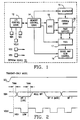
- the device is implemented as a 1K (128 x 8) bit serial EEPROM 10 with I 2 C compatibility.
- EEPROM 10 has a data line pin SDA, for serial address/data coupled to an input/output (I/O)) control logic 12, a serial clock line pin SCL also coupled to the I/O control logic, and another serial clock pin VCLK similarly coupled to the I/O control logic.
- the VCLK pin is for the transmit-only mode
- the SCL pin is for the bi-directional mode, of the EEPROM device.
- the input voltage level on each of these pins may be high or low, with resulting operation described below.
- Pins VCC and VSS provide electrical power supply (battery, e.g., +2.5V to 5.5V) and ground, respectively, relative to the battery VDD (not shown).
- I/O control logic 12 communicates with a memory control logic 14 which supplies inputs to an HV (high voltage) generator 15, an XDEC (X-line decoder) 16 and a YDEC (Y-line decoder) 17.
- Control logic 12 communicates bidirectionally with a sense amplifier R/W (read/write) control 19.
- XDEC 16 and YDEC 17 control the EEPROM array 20 with page latches 21.
- YDEC 17 also communicates with sense AMP R/W control 19.
- EEPROM device 10 is fabricated using CMOS process technology, for low power, nonvolatile memory applications.
- the device may be packaged, for example, in an 8 pin (three pins not used) PDIP (plastic dual in-line package) or SOIC (small outline integrated circuit) package.
- the device is particularly implemented for use in applications requiring storage and serial transmission of configuration and control information, with selective operation in each of two modes -- transmit-only and bi-directional. Separate two wire protocols support the two modes, each with a separate clock input as pointed out above, and sharing the common SDA data line.
- the device Upon power-up, the device automatically enters (i.e., defaults to) the transmit-only mode, in which it transmits a serial data bit stream of the entire EEPROM array 20 contents on the SDA pin, clocked by the clock signal on the VCLK. During this time the SCL pin is held high (i.e, at a logic high level).
- the separate clock lines VCLK and SCL for transmit-only mode and bi-directional mode, respectively, are also utilized to effect switching between the two modes, as desired. To that end, once the device enters the transmit-only mode it remains in that mode for so long as the SCL pin is held high. Switching of the device from the transmit-only mode to the bi-directional mode is effected by an externally induced high level to low level voltage transition on the SCL input pin. This SCL line transition is recognized by the device to cause it to switch automatically to the bi-directional mode, with byte-selectable read/write capability of the EEPROM array. When the device is in the bi-directional mode, it may be switched back to the transmit-only mode only by removing power from the device.
- the transmit-only mode of the device supports a unidirectional two wire protocol for transmission of the contents of the memory array.
- Valid data is sent only after device initialization (described below), with transmission on the SDA pin (line) in 8-bit bytes, followed by a ninth bit --a null bit -- as illustrated in the graph of FIG. 2, showing the voltage levels on (i.e., state or status of) pins VCLK, SDA, and SCL relative to time.
- the clock source for this mode is provided on the VCLK pin, with a data bit being output on the rising edge of each clock pulse.
- the parameter TVAA represents an elapsed time interval for validation of the input signal to the chip on the VCLK line, between the rising edge (e.g., 25) of the VCLK pin and the output of the data bit (e.g., bit 1) on the SDA line.
- the eight bits in each byte of data are transmitted on the SDA line in the sequence of most significant bit first.
- Each byte within the EEPROM array 20 is output in sequence. When the last byte in the array is transmitted, the output wraps around to the first location and continues.
- the SCL pin is held high (e.g., at 27) to maintain the EEPROM device in the transmit-only mode.
- FIG. 3 An exemplary initialization procedure of the device is illustrated in the graph of FIG. 3. After the power supply VCC has stabilized, the device enters the transmit-only mode. Several clock cycles (nine in this particular example) on the VCLK pin must be given to the device for performance of internal synchronization. As previously noted and as will be explained in greater detail below, because the device effectively employs only one main chip clock accommodate any of the serial data transmission modes, it is only necessary to perform internal synchronization once during device operation, and that is done during the power-up interval. This represents a significant contribution to device speed and to smooth transition from one mode to another.
- the SDA pin is in a high impedance state.
- the memory device On the rising edge of the tenth clock cycle, the memory device outputs the first valid data bit, which is the most significant bit of a byte from the EEPROM array 20. Power-up takes place at an indeterminate byte address, and the interval TVPU (illustrated on the VCLK line) between the commencement of the high impedance state of the SDA pin and the first clock cycle constitutes the power-up time for the transmit-only mode. After that, but before the first data bit is output from the array, the device proceeds through its internal synchronization.
- the device is switched from the transmit-only mode to the bi-directional mode by applying a valid high to low transition on the SCL clock pin.
- the VCLK input to the device is disregarded except that a logic high level on that pin enables a capability of an external device with bus access to write to the EEPROM.
- the bi-directional mode of the device supports a two wire bi-directional data bus transmission protocol, in which a device that sends data on the bus is defined as the transmitter, and a device that receives data from the bus is defined as the receiver.
- the EEPROM memory device 10 acts as the slave, and the bus is controlled by a master device that generates the SCL logic levels and bi-directional mode clock, controls access to the bus, and generates start and stop conditions for data transfer.
- Both master and slave may operate as transmitter or receiver, but the master determines which mode is activated and controls access to the bus.
- the bi-directional mode bus protocol allows data transfer to be initiated only when the bus is not busy (the "not busy" status of the bus being defined when both the data and the clock lines remain high), and during data transfer the data line (SDA) must remain stable whenever the clock (SCL) line is high. Changes in the SDA line while the SCL pin is high are interpreted as a start or a stop condition.
- a start data transfer condition is presented in part (B), where a start condition (which must precede all commands) is determined by the existence of a high to low transition of the SDA line while the SCL clock line is high.
- a stop data transfer condition is presented in part (C), where a stop condition (which must occur in order to end all operations) is determined by the existence of a low to high transition of the SDA line while the SCL clock line is high.
- a valid data situation is shown in part (D) of FIG. 5.
- the state of the SDA line represents valid data when, after a start condition, the SDA line is stable for the duration of the high period of the SCL clock signal.
- the data on the SDA line is allowed to change only during the low period of the SCL clock signal.
- One clock pulse is present per bit of data.
- Each data transfer is initiated with a start condition and terminated with a stop condition.
- the number of data bytes transmitted between start and stop conditions is determined by the master device and is theoretically unlimited. In the case of a write operation, where data is transmitted by the master device for storage in the EEPROM array during the bi-directional mode, only the last eight data bytes will be stored.
- only one main clock source is provided for the chip, with selective multiplexing of one or the other of the serial clock lines, depending upon the desired data transmission mode, as the main clock to accommodate the two modes of the device.
- all data transmissions from the memory device, regardless of mode are essentially synchronized to the same source.
- the device can accommodate only one data mode at any given instant of time, competition between the two modes for the clock, and interference between the them that might otherwise corrupt the data transmissions on the SDA line when either mode is operative, is nonexistent.
- the chip defaults to the transmit-only mode, and the multiplexing directs the VCLK input to the EEPROM device (i.e., the clock frequency, e.g., 60 Hertz, on the VCLK pin) to act as the main clock of the chip in which the device is fabricated.
- the multiplexed operation switches the chip from the transmit-only mode to the bi-directional mode by supplying the clock signal input on the SCL pin to provide the single main clock of the chip.
- the VCLK clock is restored for the main clock.
- a multiplexer (mux) 35 is fabricated in the EEPROM device 10 (the integrated circuit chip) to receive inputs from the SCL and VCLK pins.
- the output 37 of the multiplexer is applied as a single main clock of the chip.
- the multiplexer itself is controlled from a mode select block 40.
- the device 10 When powered on, the device 10 automatically defaults to a preselected mode (FIGS. 2, 3) -- the transmit-only mode in the embodiment which has been described herein.
- FIGS. 2, 3 the transmit-only mode in the embodiment which has been described herein.
- the SCL pin FIG. 4
- the device reverts to another mode --the bi-directional mode, which is the only other data transmission mode in this embodiment -- and cannot return to the first mode unless and until the EEPROM device is again powered on.
- both VCLK and SCL are inputs to the respective correspondingly labeled pins of the chip (FIG. 1).
- a constant frequency is applied to the VCLK pin externally of the chip -- from a video card (not shown), for example, in the case where the intelligent peripheral is a monitor (not shown) -- and that clock signal essentially "runs" or drives the chip.
- the chip sends out a data bit from the EEPROM array on the SDA pin (FIG. 2). While this is occurring, the SCL pin is maintained at a constant logic high level. If the SCL pin is taken from that high level to a logic low level (FIG.
- the VCLK clock signal will continue to be applied as an input to the chip on the VCLK pin, but the multiplexer 35 will have been switched to the SCL pin and thereby prevent the VCLK signal from going to any other point in the chip.
- the SCL line runs the main chip clock.
- the chip When the SCL pin goes from high to low, the chip ceases outputting data and briefly assumes a standby condition, from which point -- until the chip is powered off-- only clock pulses on the SCL pin will drive the chip output. From the instant of time at which the SCL line drives the main clock, the ongoing VCLK pin clock input signal (e.g., 60 Hz example) is ignored.
- the ongoing VCLK pin clock input signal e.g. 60 Hz example
- the mode select circuit 40 preferably consists essentially of an edge detector 41 which detects a high to low transition edge. If the edge detector encounters an SCL low level to high level transition, no mode switching will occur. But if the SCL later drops low, a high to low edge is detected and triggers mode switching by a signal from the mode select circuit to the multiplexer.
- the I 2 C SCL and SDA lines have pull-up resistors; if the SCL pin were to come up later than VDD (chip power), the edge detector would see a low to high transition on the SCL line -- which it would ignore --and the EEPROM device would remain in the transmit-only mode.
- a steady data stream is transmitted via the SDA line in one direction to a host device in the transmit-only mode, and in either direction in the bi-directional mode as controlled by the host.
Landscapes
- Engineering & Computer Science (AREA)
- Theoretical Computer Science (AREA)
- Physics & Mathematics (AREA)
- General Engineering & Computer Science (AREA)
- General Physics & Mathematics (AREA)
- Information Transfer Systems (AREA)
- Read Only Memory (AREA)
- Dram (AREA)
Description
(or simply, I2C-compatible) device incorporates an on-chip interface for communication directly with other such devices by means of an I2C bus, to avoid interfacing problems between chips of otherwise unrelated or only slightly related designs.
Claims (16)
- An inter integrated circuit bus-compatible, serial, electrically erasable programmable read-only memory henceforth referred to as EEPROM, device (10) for storage and serial transmission of configuration information for intelligent peripheral device with which the EEPROM device (10) is to be associated, for communication of the information on a bus to a host device, comprising:An EEPROM array (20) for storing data representing the configuration and control information, andMeans (35, 40) for selectively establishing any of a plurality of modes supported by said EEPROM device (10) for transmitting data stored in the EEPROM array (20) sequentially onto the bus in the established mode to the exclusion of all other modes for allowing interaction between said host device and said peripheral device, including separate clock input lines (VCLK, SCL) to said EEPROM device (10) each associated with a respective distinct and different one of said modes and a data line (SDA) for outputting data from the EEPROM array (20) onto the bus as clocked by the respective clock input line (VCLK, SCL) for the established mode, said means (35, 40) for selectively establishing including means (35, 40) for multiplexing said separate clock input lines (VCLK, SCL) to the EEPROM device (10) to select one of the clock input lines (VCLK, SCL) as a single clock source of the device (10) according to the mode to be established.
- The EEPROM device (10) of claim 1, wherein:
said means (35, 40) for multiplexing includes a multiplexer (35) and mode switching means (40) for controlling the multiplexer (35) to switch modes. - The EEPROM device (10) of claim 2, wherein:
said mode switching means (40) is responsive to a transitioning signal on one of said clock input lines (VCLK, SCL) provoked by a bus communication from said host device, to evoke control of the multiplexer (35). - The EEPROM device (10) of claim 2, wherein:
said mode switching means (40) is an edge detector for response to a logic level transition on said one clock input line to evoke control of the multiplexer (35). - The EEPROM device (10) of claim 1, wherein:said means (35, 40) for selectively establishing any of a plurality of modes is adapted to establish either of only two modes, one of which allows said EEPROM array (20) to be read only to output data provoked by clock signal from said single clock source, and the other of which allows said EEPROM array (20) to be read or written to, andsaid read only mode is a default mode of the EEPROM device (10).
- A method of transmitting a stream of data representing configuration information for an intelligent peripheral device from a programmable data memory device (10) associated with the peripheral device, for communication on a bus to a host device, comprising the memory device-implemented steps of:receiving said data for storage in an array (20) of said memory device (10), andselectively establishing any of a plurality of modes supported by said memory device (10) for transmitting data stored in said array (20) sequentially onto the bus in the established mode to the exclusion of all other modes for allowing interaction between said host device and said peripheral device, with separate clock input lines (VCLK, SCL) to the memory device (10) associated with respective distinct and different modes and a data line (SDA) for outputting data from the array (20) onto the bus as clocked by the respective clock input line for the established mode, including multiplexing said separate clock input lines (VCLK, SCL) to the memory device (10) to select one of the clock input lines (VCLK, SCL) as a single clock source of the device (10) according to the mode to be established.
- The method of claim 6, further including:
switching from one of said modes to another in response to a predetermined transitioning signal on one of the clock input lines (VCLK, SCL). - The method of claim 7, further including:
recognizing said transitioning signal communicated on the bus from said host device. - The method of claim 7, further including:
detecting a prescribed edge (41) of said transitioning signal as a command to switch modes. - The method of claim 6, including:
setting the initial mode of the memory device (10) following start-up of the memory device (10), as a default mode of the memory device (10). - The method of claim 10, including:
selectively establishing only two modes of data transmission for the memory device (10), one of which allows the memory device (10) to only transmit data stored in the array (20), and the other of which allows said memory device (10) to both transmit data and receive and store new data in the array (20), and setting the transmit-only mode as the default mode of the memory device (10). - A memory device (10) adapted to be programmed to store predetermined data in a memory array (20) of the device (10) for defining the configuration of an associated peripheral device to a host device coupled for communication with said memory device (10) and adapted to control said peripheral device, the memory device (10) comprising:first means (20) for storing said data,second means for delivering said data sequentially from said first means (20) to a bus for communication to said host device,third means for independently supplying clock pulses on any of a plurality of input clock lines (VCLK, SCL) to clock said data for transmission on said bus in any of a plurality of selectable modes associated with respective ones of said plurality of clock lines (VCLK, SCL),fourth means for selectively switching from one of said modes to another of said modes by recognizing a transitioning logic level on a clock line other than the clock line being used to clock said data, andfifth means (35) for restricting the supplying of said clock pulses on said plurality of input clock lines to a single clock source regardless of the mode selected for transmission of the data on said bus.
- The memory device (10) of claim 12, wherein:
Said host device is a personal computer and said peripheral device is a monitor having a display. - The memory device (10) of claim 12, wherein:
said single clock source is adapted for internal synchronization of said memory device (10). - The memory device (10) of claim 12, wherein:
said fifth means includes a multiplexer (35) controlled at least in part by said transitioning logic level to evoke a switch from an initial transmit-only default mode. - The memory device (10) of claim 15, wherein:
said fifth means includes an edge detector (40) for recognizing said transitioning logic level to control said multiplexer (35).
Applications Claiming Priority (3)
| Application Number | Priority Date | Filing Date | Title |
|---|---|---|---|
| US08/266,948 US5513334A (en) | 1994-06-27 | 1994-06-27 | Memory device with switching of data stream modes |
| US266948 | 1994-06-27 | ||
| PCT/US1995/007982 WO1996000420A1 (en) | 1994-06-27 | 1995-06-22 | Memory device with switching of data stream modes |
Publications (3)
| Publication Number | Publication Date |
|---|---|
| EP0715736A1 EP0715736A1 (en) | 1996-06-12 |
| EP0715736A4 EP0715736A4 (en) | 1996-12-27 |
| EP0715736B1 true EP0715736B1 (en) | 2000-08-30 |
Family
ID=23016641
Family Applications (1)
| Application Number | Title | Priority Date | Filing Date |
|---|---|---|---|
| EP95924675A Expired - Lifetime EP0715736B1 (en) | 1994-06-27 | 1995-06-22 | Memory device with switching of data stream modes |
Country Status (8)
| Country | Link |
|---|---|
| US (1) | US5513334A (en) |
| EP (1) | EP0715736B1 (en) |
| JP (1) | JP2834330B2 (en) |
| KR (1) | KR0178106B1 (en) |
| DE (1) | DE69518611T2 (en) |
| DK (1) | DK0715736T3 (en) |
| TW (1) | TW327212B (en) |
| WO (1) | WO1996000420A1 (en) |
Families Citing this family (33)
| Publication number | Priority date | Publication date | Assignee | Title |
|---|---|---|---|---|
| US6121949A (en) * | 1994-03-17 | 2000-09-19 | Cirrus Logic, Inc. | Method and apparatus for automatically maintaining a predetermined image quality in a display system |
| US5606715A (en) * | 1995-06-26 | 1997-02-25 | Motorola Inc. | Flexible reset configuration of a data processing system and method therefor |
| US5623687A (en) * | 1995-06-26 | 1997-04-22 | Motorola | Reset configuration in a data processing system and method therefor |
| US5841996A (en) * | 1995-10-13 | 1998-11-24 | Microchip Technology Incorporated | Serial communication interface system having programmable microcontroller for use in a battery pack |
| JPH10133995A (en) * | 1996-05-13 | 1998-05-22 | Sun Microsyst Inc | Method and apparatus for selecting optimal capabilities between a computer system and peripheral devices |
| US5878234A (en) * | 1996-09-10 | 1999-03-02 | Sierra Wireless, Inc. | Low power serial protocol translator for use in multi-circuit board electronic systems |
| DE69728578T2 (en) * | 1997-12-18 | 2004-09-30 | Thomson Consumer Electronics, Inc., Indianapolis | High speed data bus driver |
| US6693678B1 (en) | 1997-12-18 | 2004-02-17 | Thomson Licensing S.A. | Data bus driver having first and second operating modes for coupling data to the bus at first and second rates |
| US6363437B1 (en) * | 1999-01-07 | 2002-03-26 | Telefonaktiebolaget Lm Ericsson (Publ) | Plug and play I2C slave |
| FR2799045B1 (en) * | 1999-09-29 | 2002-02-08 | St Microelectronics Sa | INTEGRATED CIRCUIT MEMORY WITH SERIAL ACCESS |
| EP1513059A1 (en) * | 2003-09-08 | 2005-03-09 | Barco N.V. | A pixel module for use in a large-area display |
| JP4791696B2 (en) | 2004-03-02 | 2011-10-12 | オンセミコンダクター・トレーディング・リミテッド | Data transfer memory and module |
| KR100613606B1 (en) * | 2004-06-25 | 2006-08-21 | 삼성전자주식회사 | Optional apparatus and control method of an image forming apparatus that sets its own driving conditions using the received specification information of the main body |
| JP4593196B2 (en) * | 2004-07-29 | 2010-12-08 | シチズンホールディングス株式会社 | Semiconductor device |
| US20080036714A1 (en) * | 2004-08-30 | 2008-02-14 | Sharp Kabushiki Kaisha | Display Control Device, Display Apparatus, Method of Controlling Display Device, Display Control Program, and Storage Medium Storing the Program |
| JPWO2006025326A1 (en) * | 2004-08-31 | 2008-05-08 | シャープ株式会社 | Viewing angle control device, display device, viewing angle control device control method, viewing angle control program, and recording medium recording the program |
| US7834834B2 (en) * | 2004-09-07 | 2010-11-16 | Sharp Kabushiki Kaisha | Display device, viewing angle control device, and electronic apparatus |
| WO2006030702A1 (en) * | 2004-09-15 | 2006-03-23 | Sharp Kabushiki Kaisha | Display, viewing angle controller and electronic apparatus |
| US8031273B2 (en) * | 2004-09-17 | 2011-10-04 | Sharp Kabushiki Kaisha | Display device, viewing angle control device, and electronic device |
| WO2006038574A1 (en) * | 2004-10-04 | 2006-04-13 | Sharp Kabushiki Kaisha | Display and electronic device |
| JP4543880B2 (en) * | 2004-10-27 | 2010-09-15 | ソニー株式会社 | Memory device |
| US9660808B2 (en) * | 2005-08-01 | 2017-05-23 | Schneider Electric It Corporation | Communication protocol and method for authenticating a system |
| US7796589B2 (en) * | 2005-08-01 | 2010-09-14 | American Power Conversion Corporation | Communication protocol |
| CN100517279C (en) * | 2005-12-01 | 2009-07-22 | 鸿富锦精密工业(深圳)有限公司 | Data fatching apparatus and method |
| EP2077025A2 (en) * | 2006-08-15 | 2009-07-08 | Nxp B.V. | Device with an eeprom having both a near field communication interface and a second interface |
| CN101568907B (en) * | 2006-12-20 | 2011-04-13 | Nxp股份有限公司 | Clock generation for memory accesses without a local oscillator |
| US8549198B2 (en) * | 2009-03-27 | 2013-10-01 | Schneider Electric It Corporation | Communication protocol |
| US8194480B2 (en) * | 2009-11-19 | 2012-06-05 | Himax Technologies Limited | Method for initializing memory device |
| CN102087880B (en) * | 2009-12-08 | 2013-09-18 | 奇景光电股份有限公司 | Initialization method of memory element |
| FR3006097A1 (en) | 2013-05-21 | 2014-11-28 | St Microelectronics Rousset | MECHANISM FOR WRITING A MEMORY EEPROM ON I2C BUS |
| FR3006094A1 (en) | 2013-05-21 | 2014-11-28 | St Microelectronics Rousset | WRITING A MEMORY EEPROM ON I2C BUS |
| US9582457B2 (en) * | 2013-06-12 | 2017-02-28 | Qualcomm Incorporated | Camera control interface extension bus |
| WO2020232582A1 (en) * | 2019-05-17 | 2020-11-26 | 华为技术有限公司 | Integrated circuit having interface multiplexing functionality and pin switching method |
Family Cites Families (7)
| Publication number | Priority date | Publication date | Assignee | Title |
|---|---|---|---|---|
| US4713756A (en) * | 1985-02-28 | 1987-12-15 | Westinghouse Electric Corp. | Non-volatile memory device for a programmable controller |
| JPS63184184A (en) * | 1987-01-26 | 1988-07-29 | Tokyo Keiki Co Ltd | Memory package system |
| US4841485A (en) * | 1987-11-05 | 1989-06-20 | International Business Machines Corporation | Read/write memory device with an embedded read-only pattern and method for providing same |
| JPH01123269U (en) * | 1988-02-16 | 1989-08-22 | ||
| US5053990A (en) * | 1988-02-17 | 1991-10-01 | Intel Corporation | Program/erase selection for flash memory |
| US5070500A (en) * | 1988-08-30 | 1991-12-03 | Tokyo Keiki Company Ltd. | Memory package system utilizing inductive coupling between memory module and read/write unit |
| US5159672A (en) | 1989-12-28 | 1992-10-27 | Intel Corporation | Burst EPROM architecture |
-
1994
- 1994-06-27 TW TW083105921A patent/TW327212B/en not_active IP Right Cessation
- 1994-06-27 US US08/266,948 patent/US5513334A/en not_active Expired - Lifetime
-
1995
- 1995-06-22 WO PCT/US1995/007982 patent/WO1996000420A1/en not_active Ceased
- 1995-06-22 JP JP8503348A patent/JP2834330B2/en not_active Expired - Lifetime
- 1995-06-22 KR KR1019960700962A patent/KR0178106B1/en not_active Expired - Fee Related
- 1995-06-22 EP EP95924675A patent/EP0715736B1/en not_active Expired - Lifetime
- 1995-06-22 DK DK95924675T patent/DK0715736T3/en active
- 1995-06-22 DE DE69518611T patent/DE69518611T2/en not_active Expired - Lifetime
Also Published As
| Publication number | Publication date |
|---|---|
| WO1996000420A1 (en) | 1996-01-04 |
| TW327212B (en) | 1998-02-21 |
| JP2834330B2 (en) | 1998-12-09 |
| DE69518611D1 (en) | 2000-10-05 |
| JPH09503610A (en) | 1997-04-08 |
| EP0715736A1 (en) | 1996-06-12 |
| DE69518611T2 (en) | 2001-05-03 |
| EP0715736A4 (en) | 1996-12-27 |
| US5513334A (en) | 1996-04-30 |
| DK0715736T3 (en) | 2001-01-02 |
| KR0178106B1 (en) | 1999-05-15 |
| KR960704274A (en) | 1996-08-31 |
Similar Documents
| Publication | Publication Date | Title |
|---|---|---|
| US5513334A (en) | Memory device with switching of data stream modes | |
| US6597197B1 (en) | I2C repeater with voltage translation | |
| JP4649009B2 (en) | Information processing apparatus having a card interface, card-type electronic equipment that can be mounted on the apparatus, and operation mode setting method in the apparatus | |
| EP1576482B1 (en) | Active termination control through on module register | |
| JP7179073B2 (en) | Initialization methods and associated controllers, memory devices, and hosts | |
| US6347367B1 (en) | Data bus structure for use with multiple memory storage and driver receiver technologies and a method of operating such structures | |
| US20030056050A1 (en) | Card device | |
| EP0893767A2 (en) | A method for flexible multiple access on a serial bus by a plurality of boards | |
| JPH08180013A (en) | Computer system,method for reconfiguration of configuration register of pci bus device in response to change in pci bus clock signal frequency and method in which pci bus interfacenotifies operator of operating speed different from pci bus | |
| US6269416B1 (en) | Adaptive PCI slot | |
| EP2226729A1 (en) | Card identification compatibility | |
| US6209022B1 (en) | Slave station with two output circuits commonly and directly connected to a line for serially transmitting data to a master station in two operational modes | |
| JP5789759B2 (en) | Information processing apparatus, nonvolatile storage device, information processing system, and nonvolatile memory controller | |
| US6412023B1 (en) | System for communicating status via first signal line in a period of time in which control signal via second line is not transmitted | |
| US20050060469A1 (en) | Memory device operable with a plurality of protocols with configuration data stored in non-volatile storage elements | |
| US6868456B2 (en) | Universal serial bus device initialized with a real descriptor stored in host and method for initializing the same | |
| US20070250652A1 (en) | High speed dual-wire communications device requiring no passive pullup components | |
| US20050235110A1 (en) | Method, device and memory controller for adapting data transfer bus | |
| US5831849A (en) | Data control system | |
| TW200537271A (en) | A motherboard having a non-volatile memory which is reprogrammable through a video display port and a non-volatile memory switchable between two communication protocols | |
| JP2002245428A (en) | Multi-function card having a plurality of functions, single-function chip used for the card, and method of configuring multi-function card | |
| KR100791464B1 (en) | Display device and control method | |
| KR0135895B1 (en) | Interface device using multiple ID ports | |
| US6964045B1 (en) | Multiple program storage within a programmable logic controller system | |
| US6055609A (en) | Apparatus and method for improving bus usage in a system having a shared memory |
Legal Events
| Date | Code | Title | Description |
|---|---|---|---|
| PUAI | Public reference made under article 153(3) epc to a published international application that has entered the european phase |
Free format text: ORIGINAL CODE: 0009012 |
|
| AK | Designated contracting states |
Kind code of ref document: A1 Designated state(s): DE DK FR GB IT NL SE |
|
| 17P | Request for examination filed |
Effective date: 19960625 |
|
| RHK1 | Main classification (correction) |
Ipc: G11C 7/00 |
|
| A4 | Supplementary search report drawn up and despatched |
Effective date: 19961112 |
|
| AK | Designated contracting states |
Kind code of ref document: A4 Designated state(s): DE DK FR GB IT NL SE |
|
| 17Q | First examination report despatched |
Effective date: 19981214 |
|
| GRAG | Despatch of communication of intention to grant |
Free format text: ORIGINAL CODE: EPIDOS AGRA |
|
| GRAG | Despatch of communication of intention to grant |
Free format text: ORIGINAL CODE: EPIDOS AGRA |
|
| GRAH | Despatch of communication of intention to grant a patent |
Free format text: ORIGINAL CODE: EPIDOS IGRA |
|
| GRAH | Despatch of communication of intention to grant a patent |
Free format text: ORIGINAL CODE: EPIDOS IGRA |
|
| GRAA | (expected) grant |
Free format text: ORIGINAL CODE: 0009210 |
|
| AK | Designated contracting states |
Kind code of ref document: B1 Designated state(s): DE DK FR GB IT NL SE |
|
| REF | Corresponds to: |
Ref document number: 69518611 Country of ref document: DE Date of ref document: 20001005 |
|
| ITF | It: translation for a ep patent filed | ||
| REG | Reference to a national code |
Ref country code: DK Ref legal event code: T3 |
|
| ET | Fr: translation filed | ||
| PLBE | No opposition filed within time limit |
Free format text: ORIGINAL CODE: 0009261 |
|
| STAA | Information on the status of an ep patent application or granted ep patent |
Free format text: STATUS: NO OPPOSITION FILED WITHIN TIME LIMIT |
|
| 26N | No opposition filed | ||
| REG | Reference to a national code |
Ref country code: GB Ref legal event code: IF02 |
|
| PGFP | Annual fee paid to national office [announced via postgrant information from national office to epo] |
Ref country code: FR Payment date: 20020530 Year of fee payment: 8 |
|
| PGFP | Annual fee paid to national office [announced via postgrant information from national office to epo] |
Ref country code: SE Payment date: 20020531 Year of fee payment: 8 |
|
| PGFP | Annual fee paid to national office [announced via postgrant information from national office to epo] |
Ref country code: DK Payment date: 20020603 Year of fee payment: 8 |
|
| PGFP | Annual fee paid to national office [announced via postgrant information from national office to epo] |
Ref country code: GB Payment date: 20020619 Year of fee payment: 8 |
|
| PG25 | Lapsed in a contracting state [announced via postgrant information from national office to epo] |
Ref country code: GB Free format text: LAPSE BECAUSE OF NON-PAYMENT OF DUE FEES Effective date: 20030622 |
|
| PG25 | Lapsed in a contracting state [announced via postgrant information from national office to epo] |
Ref country code: SE Free format text: LAPSE BECAUSE OF NON-PAYMENT OF DUE FEES Effective date: 20030623 |
|
| PG25 | Lapsed in a contracting state [announced via postgrant information from national office to epo] |
Ref country code: DK Free format text: LAPSE BECAUSE OF NON-PAYMENT OF DUE FEES Effective date: 20030630 |
|
| REG | Reference to a national code |
Ref country code: DK Ref legal event code: EBP |
|
| EUG | Se: european patent has lapsed | ||
| GBPC | Gb: european patent ceased through non-payment of renewal fee |
Effective date: 20030622 |
|
| PG25 | Lapsed in a contracting state [announced via postgrant information from national office to epo] |
Ref country code: FR Free format text: LAPSE BECAUSE OF NON-PAYMENT OF DUE FEES Effective date: 20040227 |
|
| REG | Reference to a national code |
Ref country code: FR Ref legal event code: ST |
|
| PG25 | Lapsed in a contracting state [announced via postgrant information from national office to epo] |
Ref country code: IT Free format text: LAPSE BECAUSE OF NON-PAYMENT OF DUE FEES Effective date: 20050622 |
|
| PGFP | Annual fee paid to national office [announced via postgrant information from national office to epo] |
Ref country code: DE Payment date: 20140627 Year of fee payment: 20 Ref country code: NL Payment date: 20140626 Year of fee payment: 20 |
|
| REG | Reference to a national code |
Ref country code: DE Ref legal event code: R071 Ref document number: 69518611 Country of ref document: DE |
|
| REG | Reference to a national code |
Ref country code: NL Ref legal event code: V4 Effective date: 20150622 |