EP0714170A2 - Analog-to-digital converter with writable result register - Google Patents
Analog-to-digital converter with writable result register Download PDFInfo
- Publication number
- EP0714170A2 EP0714170A2 EP95308282A EP95308282A EP0714170A2 EP 0714170 A2 EP0714170 A2 EP 0714170A2 EP 95308282 A EP95308282 A EP 95308282A EP 95308282 A EP95308282 A EP 95308282A EP 0714170 A2 EP0714170 A2 EP 0714170A2
- Authority
- EP
- European Patent Office
- Prior art keywords
- analog
- signal
- result register
- digital signal
- result
- Prior art date
- Legal status (The legal status is an assumption and is not a legal conclusion. Google has not performed a legal analysis and makes no representation as to the accuracy of the status listed.)
- Granted
Links
Images


Classifications
-
- H—ELECTRICITY
- H03—ELECTRONIC CIRCUITRY
- H03M—CODING; DECODING; CODE CONVERSION IN GENERAL
- H03M1/00—Analogue/digital conversion; Digital/analogue conversion
- H03M1/12—Analogue/digital converters
-
- H—ELECTRICITY
- H03—ELECTRONIC CIRCUITRY
- H03M—CODING; DECODING; CODE CONVERSION IN GENERAL
- H03M1/00—Analogue/digital conversion; Digital/analogue conversion
- H03M1/10—Calibration or testing
- H03M1/1071—Measuring or testing
- H03M1/108—Converters having special provisions for facilitating access for testing purposes
-
- G—PHYSICS
- G01—MEASURING; TESTING
- G01R—MEASURING ELECTRIC VARIABLES; MEASURING MAGNETIC VARIABLES
- G01R31/00—Arrangements for testing electric properties; Arrangements for locating electric faults; Arrangements for electrical testing characterised by what is being tested not provided for elsewhere
- G01R31/28—Testing of electronic circuits, e.g. by signal tracer
- G01R31/3167—Testing of combined analog and digital circuits
Definitions
- the present invention relates to an analog-to-digital converter, more particularly to the register access capabilities of an analog-to-digital.
- ADCs Analog-to-digital converters, commonly referred to as ADCs, are used to digitize continuously varying voltages or other analog quantities in a wide variety of electronic devices.
- a conventional ADC includes a read-only register, referred to hereinafter as a result register, for storing the digitized data. After each conversion, the ADC automatically loads the conversion result into the result register, from which the result can be read by an external device.
- a disadvantage of the conventional ADC is that because the result register is a read-only register, it is extremely hard to test.
- the only way to test the result register is to supply the ADC with various known analog inputs, have the ADC convert each analog input, and check that the correct result can be read from the result register. Besides requiring an analog signal generator, this test procedure can take considerable time, because in most types of ADCS the conversion process itself takes time.
- This test procedure also lacks accuracy, because of the difficulty of generating precise analog signals.
- the least significant bit of the result register is especially hard to test for this reason.
- zero- or full-scale error in the ADC may prevent certain desired test data, such as data with all zero-valued bits or all one-valued bits, from being generated at all.
- ADCs are commonly tested under the assumption that the result register is operating normally. This assumption is not always true: wafer defects, photolithography defects, or ambient dust particles in the fabrication process may lead to such transistor faults as current leakage, failure to turn on or off correctly, failure to operate at high temperatures, failure to operate at high frequencies, or failure to operate at certain voltage levels. In the result register, such faults can produce incorrect read data. Bits may invert for no apparent reason, or may become stuck in the one state or zero state.
- ADCs with multiple input channels and multiple result registers are frequently built into large-scale integrated circuits such as microcontrollers.
- the analog input channels of an ADC in a microcontroller are programmable, meaning that unused analog input terminals can be assigned to other functions.
- Unused read-only result registers cannot be reassigned in this way, for they receive data only from the conversion section of the ADC. This creates another problem: waste of the microcontroller's internal register resources when not all analog input channels are used.
- Another object of the invention is to facilitate self-testing of an analog-to-digital converter in a microcontroller.
- Still another object of the invention is to permit unused result registers in an analog-to-digital converter in a microcontroller to be assigned to other functions.
- the invented analog-to-digital converter has an analog input port for receiving an external analog signal, a digital input port for receiving an external digital signal, and a control port for receiving a selection signal.
- a conversion circuit in the analog-to-digital converter converts the external analog signal to an internal digital signal.
- a selector selects either the internal digital signal or the external digital signal, responsive to the selection signal.
- the selected digital signal is stored in a result register, and can be read at a digital output port.
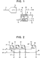
- FIG. 1 is a block diagram of a first embodiment of the invented analog-to-digital converter.
- FIG. 2 is a circuit diagram of the result register in FIG. 1.
- FIG. 3 is a circuit diagram of the buffer in FIG. 2.
- FIG. 4 is a circuit diagram of the selector in FIG. 1.
- FIG. 5 is a block diagram of a second embodiment of the invented analog-to-digital converter.
- FIG. 6 is a block diagram of a third embodiment of the invented analog-to-digital converter.
- the first embodiment is an analog-to-digital converter with a single analog input port 2 for receiving an external analog signal A, a digital input port 4 for receiving an external digital signal DE, control ports 6, 8, and 10 for receiving a selection signal SEL, a write control signal W, and a read control signal R, and a digital output port 12 for a digital output signal Q.
- Digital signals DE and Q have a data width of n bits, where n is a positive integer, so ports 4 and 12 may be parallel data ports accommodating n signal lines each.
- An analog-to-digital conversion section 14 converts the analog input signal A to an n-bit internal digital signal DI, which is output on an n-bit internal data path 16 to a selector 18.
- the selector 18 also receives the external data signal DE from input port 4, via another n-bit internal data path 20, and receives the selection signal SEL from input port 6.
- the selector 18 selects DE or DI and sends the selected signal on yet another n-bit internal data path 22 to a result register 24.
- the result register 24 stores the selected signal, DE or DI, in response to input of the write signal W, and outputs the stored signal to output port 12 in response to input of the read signal R.
- the read and select signals R and SEL are generated externally to the analog-to-digital converter.
- the write signal W can be generated externally, and can also be generated within the analog-to-digital converter, by control circuitry not shown in the drawings.
- FIG. 2 shows the circuit configuration of the result register 24.
- This register 24 has n delay flip-flops 26, each with a data input terminal D, data output terminal Q, and clock input terminal CK.
- the data input terminals D receive the n bits D1, ..., Dn of the selected digital signal via the n signal lines 22' of data path 22.
- the clock input terminal CK receives the write signal W from input port 8.
- the data output terminals Q are coupled to n buffer amplifiers 28, which are controlled by the read signal R from port 10.
- the amplifiers 28 output the n bits Q1, ..., Qn of the digital output signal Q at the n-bit output port 12, which comprises 12 individual output terminals 12'.
- FIG. 3 shows the circuit configuration of the buffer amplifiers 28 in FIG. 2.
- the first buffer amplifier 28 is shown as an example, but all n buffer amplifiers 28 have the same type of structure.
- Each buffer amplifier 28 comprises a pair of inverters 30 and 31, and four field-effect transistors 32, 34, 36, and 38 coupled in series between a power-supply terminal 39 and a ground terminal 40.
- the two transistors 32 and 34 on the ground side are n-channel metal-oxide-semiconductor (NMOS) field-effect transistors; the two transistors 36 and 38 on the power-supply side are p-channel metal-oxide-semiconductor (PMOS) field-effect transistors.
- Inverter 30 receives the data output signal from, for example, the first flip-flop 26 in FIG. 2, and controls the gates of transistors 34 and 36.
- Inverter 31 receives the read signal R and controls the gates of transistors 32 and 38.
- FIG. 4 shows the circuit configuration of a one-bit section of the selector 18.
- the selector 18 comprises n parallel sections with this structure. All sections of the selector 18 receive the selection signal SEL.
- Signal lines 16', 20', and 22' in FIG. 4 are bit lines in the corresponding data paths 16, 20, and 22 in FIG. 1.
- the circuit in FIG. 4 has a pair of two-input AND gates 41 and 42, an inverter 43, and a two-input OR gate 44.
- AND gate 41 receives the selection signal SEL, and receives one bit of the internal digital signal DI on signal line 16'.
- AND gate 42 receives the selection signal SEL as inverted by inverter 43, and receives one bit of the external digital signal DE on signal line 20'.
- OR gate 44 receives the outputs of AND gates 41 and 42, takes their logical OR, and sends the result to the result register on signal line 22'.
- the conversion circuit 14 in FIG. 1 samples the voltage of analog input signal A, quantizes the sampled voltage, and outputs an internal data signal DI representing the quantized value.
- Various methods of conversion from A to DI can be used, such as the well-known method of successive approximations.
- the invention is not restricted to any particular conversion method.
- the write signal W When conversion is completed and the correct internal digital signal DI is present on data paths 16 and 22, the write signal W is activated briefly. This write pulse causes the flip-flops 26 in FIG. 2 to latch the internal digital signal DI from data path 22 and begin output of the DI data at their output terminals Q.
- an external device such as a central processing unit (CPU, not visible) activates the read signal R by driving R high, causing transistors 32 and 38 in FIG. 3 to turn on.
- a central processing unit CPU, not visible
- the conversion result stored as an internal digital signal DI in the result register 24, is output as a digital output signal Q at output port 12.
- the data pattern to be tested is sent to digital input port 4. Since the selection signal SEL is low, selector 18 selects this data pattern and sends it to the result register 24.
- the write signal W is then activated at an appropriate timing, storing the data pattern in the result register 24 as explained above. After the write signal W has been deactivated and a certain time has elapsed, the read signal R is activated and the result register contents are read from the digital output port 12. The test passes if the read data match the written data for all patterns tested, showing that data can be written, held in the result register for a certain time, then read correctly.
- This test can be executed quickly and easily, because the desired test patterns are written directly from the digital input port 4, instead of being generated by converting equivalent analog voltages.
- the conversion section 14 can then be tested by supplying known analog input signals A and checking whether they are converted to correct output data Q. If the output data Q are not correct, it will be clear that this is due to a conversion error and not a result-register malfunction. This knowledge simplifies fault analysis and the planning of remedial action.
- This checking procedure is particularly useful when the analog-to-digital converter is built into a device such as a microcontroller that can be programmed to carry the check out automatically.
- a microcontroller that controls an automobile, for example, it is highly desirable to have analog conversion results checked in this way.
- the microcontroller can be programmed to carry out a more thorough check by reading the DX value before the next conversion begins, to verify that DX was actually written in the result register 24.
- the second embodiment is an analog-to-digital converter with multiple analog input ports or channels.
- the same reference numerals are used as in FIG. 1 to identify identical or similar elements, using hyphenated suffixes to indicate multiple elements of the same type.
- the analog input ports are numbered 2-0 to 2-m (m being a positive integer).
- analog ports 2-1 to 2-m are connected to respective analog switches 46-0 to 46-m, which are controlled by channel address signals S0 to S m .
- Analog switches 46-0 to 46-m are coupled in parallel to the conversion section 14.
- Data paths 16 and 20 are coupled in parallel to m selectors 18-0 to 18-m, all of which receive the same selection signal SEL from control port 6.
- the signals selected by the selectors are provided to respective result register 24-0 to 24-m, which are coupled in parallel to the digital output port 12.
- Result registers 24-0 to 24-m receive the write signal W from control port 8 through respective two-input AND gates 48-0 to 48-m, and receive the read signal R from control port 10 through respective two-input AND gates 49-0 to 49-m.
- the second inputs to these AND gates are the channel address signals S0 to S m .
- channel address signal S0 is driven high, turning on analog switch 46-0, and channel address signals S1 to S m are driven low, turning off analog switches 46-1 to 46-m.
- the selection signal SEL is driven high, so that all selectors 18-0 to 18-m select the internal digital signal DI.
- the conversion section 14 receives analog signal A0 through analog switch 46-0, samples this signal, and outputs a corresponding internal digital signal DI on data path 16. After conversion is completed, the write signal W is driven high for a brief pulse, as in the first embodiment.
- the read signal R is driven high.
- the output of AND gate 49-0 then goes high, while the outputs of AND gates 49-1 to 49-m remain low.
- the digital signal value stored in result register 24-0 is accordingly output at the digital output port 12.
- each conversion result it is not necessary for each conversion result to be read immediately. It is possible, for example, first to convert all of the analog input signals A0 to A m , by driving the channel address signals S0 to S m high in turn and pulsing the write signal W, then to read the conversion results at convenient times, by activating the read signal R and driving the channel address signals S0 to S m high again. It is also possible to read the conversion result of one input channel while another channel is being converted.
- Interference between registers can be detected by writing a sequence of m different test patterns in the m result registers 24-0 to 24-m, then reading the result registers in turn.
- Another type of test can be carried out by writing the same test pattern in all the result registers. The writing can be done simultaneously, if means are provided for driving all of the channel address signals high at once.
- the ability to write directly to the result registers facilitates all types of tests.
- the third embodiment is identical to the second embodiment, except that independent selection signals SEL0 to SEL m from different control ports 6-0 to 6-m are supplied to the selectors 18-0 to 18-m. A detailed description of the circuit configuration and operation will be omitted. Except for the control ports, the reference numerals are the same as in FIG. 5.
- Selection signals SEL0 to SEL m can be generated from, for example, an m-bit control register (not visible), each register bit controlling one of the selection signals. An arbitrary set of selection signals can thus be activated. Tests can be carried out by writing to this control register and issuing the appropriate read, write, and channel address signals.
- a decoder can be provided that decodes a value i, ranging from 0 to m, and activates signals SEL0 to SEL i , or decodes a pair of values (j, k) and activates signals SEL j to SEL k .
- This arrangement provides less flexibility, but requires fewer control bits.
- the third embodiment is particularly suited for use in a microcontroller.
- Input terminal 4 and output terminal 12 are linked to the microcontroller's internal data bus (not visible), so that the microcontroller's central processing unit (also not visible) can both read and write to the result registers.
- the microcontroller can be programmed to set the selection signals SEL i of the unused channels permanently to the level that selects the external digital signal DE.
- the result registers of these channels can then be employed as general-purpose data registers. Frequently-accessed flag data or other data can be stored in these registers for rapid access. Additional logic circuitry, not shown in the diagrams, can be provided to prevent collision between read and write signals at the same result register.
- the invention thus permits the microcontroller to make more complete use of its register resources than in the prior art.
- Unused analog input ports can of course also be reassigned, to general-purpose input or output of digital signals, for example, as in conventional microcontrollers.
- the present invention is not limited to the preceding embodiments, but permits various modifications.
- the number of result registers was equal to the number of analog input ports, but this need not be true in general. Two or more analog input ports can share a single result register, or a single analog input port may have multiple result registers.
- some analog input ports may have fixed assignments while others are reassignable. Selectors are still preferably provided for all result registers, to facilitate testing.
- circuit configurations shown in FIGs. 2, 3, and 4 can be modified in various obvious ways. Signals that were described as active high may be active low instead.
- Applications are not limited to ADCs that convert analog voltage inputs to equivalent digital values.
- the invention can be practiced in any device that converts any type of analog input signal to a digital output signal, including analog comparators, frequency counters, and various types of digital measuring or metering equipment.
Abstract
Description
- The present invention relates to an analog-to-digital converter, more particularly to the register access capabilities of an analog-to-digital.
- Analog-to-digital converters, commonly referred to as ADCs, are used to digitize continuously varying voltages or other analog quantities in a wide variety of electronic devices. A conventional ADC includes a read-only register, referred to hereinafter as a result register, for storing the digitized data. After each conversion, the ADC automatically loads the conversion result into the result register, from which the result can be read by an external device.
- A disadvantage of the conventional ADC is that because the result register is a read-only register, it is extremely hard to test. The only way to test the result register is to supply the ADC with various known analog inputs, have the ADC convert each analog input, and check that the correct result can be read from the result register. Besides requiring an analog signal generator, this test procedure can take considerable time, because in most types of ADCS the conversion process itself takes time.
- This test procedure also lacks accuracy, because of the difficulty of generating precise analog signals. The least significant bit of the result register is especially hard to test for this reason. To make matters worse, zero- or full-scale error in the ADC may prevent certain desired test data, such as data with all zero-valued bits or all one-valued bits, from being generated at all.
- Because of these difficulties, ADCs are commonly tested under the assumption that the result register is operating normally. This assumption is not always true: wafer defects, photolithography defects, or ambient dust particles in the fabrication process may lead to such transistor faults as current leakage, failure to turn on or off correctly, failure to operate at high temperatures, failure to operate at high frequencies, or failure to operate at certain voltage levels. In the result register, such faults can produce incorrect read data. Bits may invert for no apparent reason, or may become stuck in the one state or zero state.
- When the result register of a conventional ADC fails in this way, it becomes difficult to tell what is happening inside the ADC, hence difficult to analyze the fault. It may be impossible to determine, for example, whether the fault is in the result register, or in the conversion circuit itself. Moreover, if the fault occurs only under certain temperature, voltage, or frequency conditions, the fault may go undetected for some time. In safety-critical equipment, such as automotive electronic systems, such undetected faults can have serious consequences.
- ADCs with multiple input channels and multiple result registers are frequently built into large-scale integrated circuits such as microcontrollers. Often the analog input channels of an ADC in a microcontroller are programmable, meaning that unused analog input terminals can be assigned to other functions. Unused read-only result registers, however, cannot be reassigned in this way, for they receive data only from the conversion section of the ADC. This creates another problem: waste of the microcontroller's internal register resources when not all analog input channels are used.
- It is accordingly an object of the present invention to facilitate the testing of an analog-to-digital converter.
- Another object of the invention is to facilitate self-testing of an analog-to-digital converter in a microcontroller.
- Still another object of the invention is to permit unused result registers in an analog-to-digital converter in a microcontroller to be assigned to other functions.
- The invented analog-to-digital converter has an analog input port for receiving an external analog signal, a digital input port for receiving an external digital signal, and a control port for receiving a selection signal. A conversion circuit in the analog-to-digital converter converts the external analog signal to an internal digital signal. A selector selects either the internal digital signal or the external digital signal, responsive to the selection signal. The selected digital signal is stored in a result register, and can be read at a digital output port.
- FIG. 1 is a block diagram of a first embodiment of the invented analog-to-digital converter.
- FIG. 2 is a circuit diagram of the result register in FIG. 1.
- FIG. 3 is a circuit diagram of the buffer in FIG. 2.
- FIG. 4 is a circuit diagram of the selector in FIG. 1.
- FIG. 5 is a block diagram of a second embodiment of the invented analog-to-digital converter.
- FIG. 6 is a block diagram of a third embodiment of the invented analog-to-digital converter.
- Three embodiments of the invention will be described with reference to the attached illustrative drawings.
- Referring to FIG. 1, the first embodiment is an analog-to-digital converter with a single
analog input port 2 for receiving an external analog signal A, adigital input port 4 for receiving an external digital signal DE,control ports digital output port 12 for a digital output signal Q. Digital signals DE and Q have a data width of n bits, where n is a positive integer, soports - An analog-to-
digital conversion section 14 converts the analog input signal A to an n-bit internal digital signal DI, which is output on an n-bitinternal data path 16 to aselector 18. Theselector 18 also receives the external data signal DE frominput port 4, via another n-bitinternal data path 20, and receives the selection signal SEL frominput port 6. Theselector 18 selects DE or DI and sends the selected signal on yet another n-bitinternal data path 22 to aresult register 24. - The
result register 24 stores the selected signal, DE or DI, in response to input of the write signal W, and outputs the stored signal tooutput port 12 in response to input of the read signal R. - The read and select signals R and SEL are generated externally to the analog-to-digital converter. The write signal W can be generated externally, and can also be generated within the analog-to-digital converter, by control circuitry not shown in the drawings.
- FIG. 2 shows the circuit configuration of the
result register 24. Thisregister 24 has n delay flip-flops 26, each with a data input terminal D, data output terminal Q, and clock input terminal CK. The data input terminals D receive the n bits D1, ..., Dn of the selected digital signal via the n signal lines 22' ofdata path 22. The clock input terminal CK receives the write signal W frominput port 8. The data output terminals Q are coupled ton buffer amplifiers 28, which are controlled by the read signal R fromport 10. Theamplifiers 28 output the n bits Q1, ..., Qn of the digital output signal Q at the n-bit output port 12, which comprises 12 individual output terminals 12'. - FIG. 3 shows the circuit configuration of the
buffer amplifiers 28 in FIG. 2. Thefirst buffer amplifier 28 is shown as an example, but alln buffer amplifiers 28 have the same type of structure. - Each
buffer amplifier 28 comprises a pair ofinverters effect transistors supply terminal 39 and aground terminal 40. The twotransistors transistors Inverter 30 receives the data output signal from, for example, the first flip-flop 26 in FIG. 2, and controls the gates oftransistors Inverter 31 receives the read signal R and controls the gates oftransistors - FIG. 4 shows the circuit configuration of a one-bit section of the
selector 18. Theselector 18 comprises n parallel sections with this structure. All sections of theselector 18 receive the selection signal SEL. Signal lines 16', 20', and 22' in FIG. 4 are bit lines in thecorresponding data paths - The circuit in FIG. 4 has a pair of two-input AND
gates inverter 43, and a two-input ORgate 44. ANDgate 41 receives the selection signal SEL, and receives one bit of the internal digital signal DI on signal line 16'. ANDgate 42 receives the selection signal SEL as inverted byinverter 43, and receives one bit of the external digital signal DE on signal line 20'. ORgate 44 receives the outputs of ANDgates - Next, the operation of converting analog input A to digital output Q will be described. During this operation the selection signal SEL is driven high, enabling AND
gate 41 in FIG. 4 and disabling ANDgate 42, so thatselector 18 selects the internal digital signal DI. The read and write signals R and W are both initially inactive. - The
conversion circuit 14 in FIG. 1 samples the voltage of analog input signal A, quantizes the sampled voltage, and outputs an internal data signal DI representing the quantized value. Various methods of conversion from A to DI can be used, such as the well-known method of successive approximations. The invention is not restricted to any particular conversion method. - When conversion is completed and the correct internal digital signal DI is present on
data paths flops 26 in FIG. 2 to latch the internal digital signal DI fromdata path 22 and begin output of the DI data at their output terminals Q. - To read the conversion result, an external device such as a central processing unit (CPU, not visible) activates the read signal R by driving R high, causing
transistors inverter 30 in FIG. 3, one of the twotransistors result register 24, is output as a digital output signal Q atoutput port 12. - Next the operation of testing the data register 24 will be described. During this operation the selection signal SEL is low, disabling AND
gate 41 in FIG. 4 and enabling ANDgate 42, so thatselector 18 selects the external digital signal DE. - The test is carried out by writing various data patterns in the
result register 24 and checking whether they can be read correctly. If the data width is eight bits (n = 8), for example, the data patterns '0000 0000,' '0101 0101,' '1010 1010,' and '1111 1111' can be tested. These patterns check that a zero and a one can be written in each bit, and check for interference such as a short circuit between adjacent bit lines. - The data pattern to be tested is sent to
digital input port 4. Since the selection signal SEL is low,selector 18 selects this data pattern and sends it to theresult register 24. The write signal W is then activated at an appropriate timing, storing the data pattern in the result register 24 as explained above. After the write signal W has been deactivated and a certain time has elapsed, the read signal R is activated and the result register contents are read from thedigital output port 12. The test passes if the read data match the written data for all patterns tested, showing that data can be written, held in the result register for a certain time, then read correctly. - This test can be executed quickly and easily, because the desired test patterns are written directly from the
digital input port 4, instead of being generated by converting equivalent analog voltages. - If the result register 24 passes this test, the
conversion section 14 can then be tested by supplying known analog input signals A and checking whether they are converted to correct output data Q. If the output data Q are not correct, it will be clear that this is due to a conversion error and not a result-register malfunction. This knowledge simplifies fault analysis and the planning of remedial action. - Next, a procedure for checking the analog-to-digital converter during operation will be described. This procedure is useful when a slowly-changing analog signal, such as a signal from a temperature sensor, is converted at regular intervals.
- In this situation, if the same output data Q are obtained repeatedly, that might indicate that the analog input signal is not changing, or it might indicate that the result has become stuck at one value due to an electrical fault. Therefore, each time the output data Q are read, the value of Q is altered, e.g. by subtracting a fixed quantity, to create test data DX, which are sent to the
digital input terminal 4. The selection signal SEL is driven low and the write signal W is briefly activated, writing the altered data DX into theresult register 24. The selection signal SEL is driven high again before the next conversion ends. - When the next conversion ends and the output data Q are stored and read again, if the result is equal to DX, that raises the suspicion of a malfunction. If this happens repeatedly, the suspicion becomes a substantial certainty. Appropriate action can then be taken, such as displaying an alarm indication, halting a potentially dangerous operation, or switching over to a fail-safe mode.
- This checking procedure is particularly useful when the analog-to-digital converter is built into a device such as a microcontroller that can be programmed to carry the check out automatically. In a microcontroller that controls an automobile, for example, it is highly desirable to have analog conversion results checked in this way. The microcontroller can be programmed to carry out a more thorough check by reading the DX value before the next conversion begins, to verify that DX was actually written in the
result register 24. - Referring to FIG. 5, the second embodiment is an analog-to-digital converter with multiple analog input ports or channels. The same reference numerals are used as in FIG. 1 to identify identical or similar elements, using hyphenated suffixes to indicate multiple elements of the same type. For example, the analog input ports are numbered 2-0 to 2-m (m being a positive integer).
- The analog ports 2-1 to 2-m are connected to respective analog switches 46-0 to 46-m, which are controlled by channel address signals S₀ to Sm. Analog switches 46-0 to 46-m are coupled in parallel to the
conversion section 14. -
Data paths control port 6. The signals selected by the selectors are provided to respective result register 24-0 to 24-m, which are coupled in parallel to thedigital output port 12. - Result registers 24-0 to 24-m receive the write signal W from
control port 8 through respective two-input AND gates 48-0 to 48-m, and receive the read signal R fromcontrol port 10 through respective two-input AND gates 49-0 to 49-m. The second inputs to these AND gates are the channel address signals S₀ to Sm. - The analog-to-digital conversion operation will be described next, taking conversion of analog signal A₀ as an example.
- To convert this signal, channel address signal S₀ is driven high, turning on analog switch 46-0, and channel address signals S₁ to Sm are driven low, turning off analog switches 46-1 to 46-m. The selection signal SEL is driven high, so that all selectors 18-0 to 18-m select the internal digital signal DI.
- The
conversion section 14 receives analog signal A₀ through analog switch 46-0, samples this signal, and outputs a corresponding internal digital signal DI ondata path 16. After conversion is completed, the write signal W is driven high for a brief pulse, as in the first embodiment. - Since channel address signal S₀ is high, this write pulse W passes through AND gate 48-0 to result register 24-0, causing result register 24-0 to store the internal digital signal DI. Since the other channel address signals are low, the outputs of AND gates 48-1 to 48-m remain low, and the internal digital signal DI is not stored in result registers 24-1 to 24-m, which continue to hold their previous contents.
- When the conversion result is read, the read signal R is driven high. The output of AND gate 49-0 then goes high, while the outputs of AND gates 49-1 to 49-m remain low. The digital signal value stored in result register 24-0 is accordingly output at the
digital output port 12. - It is not necessary for each conversion result to be read immediately. It is possible, for example, first to convert all of the analog input signals A₀ to Am, by driving the channel address signals S₀ to Sm high in turn and pulsing the write signal W, then to read the conversion results at convenient times, by activating the read signal R and driving the channel address signals S₀ to Sm high again. It is also possible to read the conversion result of one input channel while another channel is being converted.
- Next various register tests will be briefly described.
- To test a particular register, it suffices to drive the corresponding channel address signal high and proceed as in the first embodiment.
- Interference between registers can be detected by writing a sequence of m different test patterns in the m result registers 24-0 to 24-m, then reading the result registers in turn.
- Another type of test can be carried out by writing the same test pattern in all the result registers. The writing can be done simultaneously, if means are provided for driving all of the channel address signals high at once.
- As in the first embodiment, the ability to write directly to the result registers facilitates all types of tests.
- Referring to FIG. 6, the third embodiment is identical to the second embodiment, except that independent selection signals SEL₀ to SELm from different control ports 6-0 to 6-m are supplied to the selectors 18-0 to 18-m. A detailed description of the circuit configuration and operation will be omitted. Except for the control ports, the reference numerals are the same as in FIG. 5.
- Selection signals SEL₀ to SELm can be generated from, for example, an m-bit control register (not visible), each register bit controlling one of the selection signals. An arbitrary set of selection signals can thus be activated. Tests can be carried out by writing to this control register and issuing the appropriate read, write, and channel address signals.
- Alternatively, a decoder can be provided that decodes a value i, ranging from 0 to m, and activates signals SEL₀ to SELi, or decodes a pair of values (j, k) and activates signals SELj to SELk. This arrangement provides less flexibility, but requires fewer control bits.
- The third embodiment is particularly suited for use in a microcontroller.
Input terminal 4 andoutput terminal 12 are linked to the microcontroller's internal data bus (not visible), so that the microcontroller's central processing unit (also not visible) can both read and write to the result registers. If it is not necessary to use all of the analog input channels in a certain application, the microcontroller can be programmed to set the selection signals SELi of the unused channels permanently to the level that selects the external digital signal DE. The result registers of these channels can then be employed as general-purpose data registers. Frequently-accessed flag data or other data can be stored in these registers for rapid access. Additional logic circuitry, not shown in the diagrams, can be provided to prevent collision between read and write signals at the same result register. - The invention thus permits the microcontroller to make more complete use of its register resources than in the prior art. Unused analog input ports can of course also be reassigned, to general-purpose input or output of digital signals, for example, as in conventional microcontrollers.
- The present invention is not limited to the preceding embodiments, but permits various modifications. In the second and third embodiments, for example, the number of result registers was equal to the number of analog input ports, but this need not be true in general. Two or more analog input ports can share a single result register, or a single analog input port may have multiple result registers.
- In a microcontroller, some analog input ports may have fixed assignments while others are reassignable. Selectors are still preferably provided for all result registers, to facilitate testing.
- The circuit configurations shown in FIGs. 2, 3, and 4 can be modified in various obvious ways. Signals that were described as active high may be active low instead.
- Applications are not limited to ADCs that convert analog voltage inputs to equivalent digital values. The invention can be practiced in any device that converts any type of analog input signal to a digital output signal, including analog comparators, frequency counters, and various types of digital measuring or metering equipment.
Claims (11)
- An analog-to-digital converter, comprising:an analog input port (2) for receiving an external analog signal;a digital input port (4) for receiving an external digital signal;a control port (6) for receiving a selection signal;a conversion circuit (14) coupled to said analog input port (2), for converting said external analog signal to an internal digital signal;a selector (18) coupled to said conversion circuit (14), for selecting one signal from among said internal digital signal and said external digital signal, responsive to said selection signal;a result register (24) coupled to said selector (18), for storing the signal selected by said selector (18); anda digital output port (12) for output of the signal stored in said result register (24).
- The analog-to-digital converter of claim 1, comprising:a plurality of selectors (18-0 to 18-m) as described in claim 1, each receiving said internal digital signal and said external digital signal; anda like plurality of result registers (24-0 to 24-m) as described in claim 1, coupled to respective selectors (18-0 to 18-m), for storing signals selected by respective selectors (18-0 to 18-m).
- The analog-to-digital converter of claim 2, further comprising a plurality of analog input ports (2-0 to 2-m) coupled to said conversion section (14) in parallel.
- The analog-to-digital converter of claim 2, comprising
a plurality of control terminals (6-0 to 6-m) as described in claim 1, coupled to respective selectors (18-0 to 18-m), for controlling said selectors (18-0 to 18-m) independently of one another. - The analog-to-digital converter of claim 1, wherein said analog-to-digital converter forms one part of a microcontroller.
- A method of testing an analog-to-digital converter having a result register (24), comprising the steps of:writing a test pattern directly in said result register (24); andreading said test pattern from said result register (24).
- The method of claim 6, comprising the further step of controlling a selection signal that has one state selecting input of an external digital signal to said result register (24), and another state selecting input of an internal digital signal to said result register (24), said internal digital signal being generated by converting an external analog signal.
- A method of testing an analog-to-digital converter having a result register (24), comprising the steps of:(a) converting an external analog signal to an internal digital signal;(b) setting a selection signal to a first state, selecting input of said internal digital signal to said result register (24);(c) storing said internal digital signal in said result register (24);(d) reading said internal digital signal from said result register (24) as a first value;(e) generating an external digital signal with a second value different from said first value;(f) setting said selection signal to a second state, selecting input of said external digital signal to said result register (24);(g) storing said external digital signal in said result register (24); and(h) repeating said steps (a) to (g).
- The method of claim 8, comprising the further steps of:reading said result register (24) after said step (g); andchecking whether said second value is read.
- A method of using an analog-to-digital converter, having multiple analog input ports (2-0 to 2-m) and corresponding result registers (24-0 to 24-m), in a microcontroller, comprising the steps of:assigning each of said analog input ports (2-0 to 2-m) to one of a plurality of functions, said functions including both input of analog signals and other functions;using those result registers corresponding to analog input ports assigned to input of said analog signals for storing conversion results of said analog input signals; andusing those result registers corresponding to analog input ports assigned to said other functions for storing general-purpose data.
- The method of claim 10, comprising the further steps of:testing said result registers corresponding to analog input ports assigned to input of said analog signals, by writing data other than said conversion results in said result registers.
Applications Claiming Priority (3)
| Application Number | Priority Date | Filing Date | Title |
|---|---|---|---|
| JP291468/94 | 1994-11-25 | ||
| JP29146894 | 1994-11-25 | ||
| JP6291468A JPH08154055A (en) | 1994-11-25 | 1994-11-25 | Analog/digital converter |
Publications (3)
| Publication Number | Publication Date |
|---|---|
| EP0714170A2 true EP0714170A2 (en) | 1996-05-29 |
| EP0714170A3 EP0714170A3 (en) | 1998-12-02 |
| EP0714170B1 EP0714170B1 (en) | 2001-10-31 |
Family
ID=17769266
Family Applications (1)
| Application Number | Title | Priority Date | Filing Date |
|---|---|---|---|
| EP95308282A Expired - Lifetime EP0714170B1 (en) | 1994-11-25 | 1995-11-20 | Analog-to-digital converter with writable result register |
Country Status (5)
| Country | Link |
|---|---|
| US (1) | US5815105A (en) |
| EP (1) | EP0714170B1 (en) |
| JP (1) | JPH08154055A (en) |
| KR (1) | KR100457033B1 (en) |
| DE (1) | DE69523537T2 (en) |
Cited By (3)
| Publication number | Priority date | Publication date | Assignee | Title |
|---|---|---|---|---|
| WO2003096540A1 (en) * | 2002-05-08 | 2003-11-20 | Continental Teves Ag & Co. Ohg | Electronic circuit arrangement for error-free analog/digital conversion of signals |
| WO2006108848A1 (en) * | 2005-04-12 | 2006-10-19 | Robert Bosch Gmbh | Converter arrangement and test method for a converter |
| WO2018129452A1 (en) * | 2017-01-06 | 2018-07-12 | Microchip Technology Incorporated | Verification, validation, and applications support for analog-to-digital converter systems |
Families Citing this family (3)
| Publication number | Priority date | Publication date | Assignee | Title |
|---|---|---|---|---|
| DE19643872A1 (en) | 1996-10-31 | 1998-05-07 | Alsthom Cge Alcatel | Optical network termination unit of a hybrid fiber optic coaxial cable access network |
| KR100531382B1 (en) * | 2003-10-25 | 2005-11-29 | 엘지전자 주식회사 | Method of fixing sampling phase in Analog-Digital Converter and Apparatus of the same |
| DE102006003566B4 (en) * | 2006-01-25 | 2020-10-01 | Infineon Technologies Ag | Signal conversion device, in particular analog-digital conversion device, and method for operating a signal conversion device |
Family Cites Families (11)
| Publication number | Priority date | Publication date | Assignee | Title |
|---|---|---|---|---|
| JPS5422557A (en) * | 1977-07-22 | 1979-02-20 | Hitachi Ltd | Constant current circuit |
| US4922492A (en) * | 1988-05-13 | 1990-05-01 | National Semiconductor Corp. | Architecture and device for testable mixed analog and digital VLSI circuits |
| DE68926191T2 (en) * | 1988-07-13 | 1996-11-28 | Nec Corp | One-chip data processor with built-in A / D converter |
| US5047770A (en) * | 1990-05-03 | 1991-09-10 | General Electric Company | Apparatus for testing data conversion/transfer functions in a vibratory energy imaging system |
| DE69125674T2 (en) * | 1990-09-04 | 1997-10-23 | Motorola Inc | Automatic analog to digital conversion with selectable format results |
| JP2553753B2 (en) * | 1990-10-17 | 1996-11-13 | 三菱電機株式会社 | AD converter |
| JPH04212524A (en) * | 1990-12-06 | 1992-08-04 | Matsushita Electric Ind Co Ltd | Semiconductor integrated circuit |
| KR930004772Y1 (en) * | 1991-05-13 | 1993-07-23 | 금성일렉트론 주식회사 | Apparatus for testing analog to digital |
| US5185607A (en) * | 1992-01-31 | 1993-02-09 | Motorola, Inc. | Method and apparatus for testing an analog to digital converter |
| US5175547A (en) * | 1992-01-31 | 1992-12-29 | Motorola, Inc. | Method and apparatus for testing an analog to digital converter |
| JPH06164391A (en) * | 1992-11-25 | 1994-06-10 | Mitsubishi Electric Corp | A/d converter |
-
1994
- 1994-11-25 JP JP6291468A patent/JPH08154055A/en not_active Withdrawn
-
1995
- 1995-11-20 DE DE69523537T patent/DE69523537T2/en not_active Expired - Lifetime
- 1995-11-20 EP EP95308282A patent/EP0714170B1/en not_active Expired - Lifetime
- 1995-11-22 US US08/562,118 patent/US5815105A/en not_active Expired - Lifetime
- 1995-11-24 KR KR1019950043633A patent/KR100457033B1/en not_active IP Right Cessation
Non-Patent Citations (1)
| Title |
|---|
| None |
Cited By (5)
| Publication number | Priority date | Publication date | Assignee | Title |
|---|---|---|---|---|
| WO2003096540A1 (en) * | 2002-05-08 | 2003-11-20 | Continental Teves Ag & Co. Ohg | Electronic circuit arrangement for error-free analog/digital conversion of signals |
| US7135998B2 (en) | 2002-05-08 | 2006-11-14 | Continental Teves Ag & Co. Ohg | Electronic circuit arrangement for error-free analog/digital conversion of signals |
| DE10392545B4 (en) | 2002-05-08 | 2018-03-15 | Continental Teves Ag & Co. Ohg | Electronic circuitry for error-proof analog-to-digital conversion of signals |
| WO2006108848A1 (en) * | 2005-04-12 | 2006-10-19 | Robert Bosch Gmbh | Converter arrangement and test method for a converter |
| WO2018129452A1 (en) * | 2017-01-06 | 2018-07-12 | Microchip Technology Incorporated | Verification, validation, and applications support for analog-to-digital converter systems |
Also Published As
| Publication number | Publication date |
|---|---|
| EP0714170B1 (en) | 2001-10-31 |
| EP0714170A3 (en) | 1998-12-02 |
| KR100457033B1 (en) | 2005-01-27 |
| KR960020008A (en) | 1996-06-17 |
| US5815105A (en) | 1998-09-29 |
| JPH08154055A (en) | 1996-06-11 |
| DE69523537T2 (en) | 2002-06-27 |
| DE69523537D1 (en) | 2001-12-06 |
Similar Documents
| Publication | Publication Date | Title |
|---|---|---|
| US5285152A (en) | Apparatus and methods for testing circuit board interconnect integrity | |
| US3961252A (en) | Testing embedded arrays | |
| KR0155180B1 (en) | Semiconductor memory device having a coincidence detection circuit and its test method | |
| EP0053665B1 (en) | Testing embedded arrays in large scale integrated circuits | |
| EP0447117B1 (en) | Built-in self test for analog to digital converters | |
| JP2650203B2 (en) | Apparatus and method for controlling operation of a plurality of test pins of semiconductor device test system | |
| EP0366553B1 (en) | Test device and method for testing electronic device and semiconductor device having the test device | |
| US5835506A (en) | Single pass doublet mode integrated circuit tester | |
| EP0222084A2 (en) | Hierarchical test system architecture | |
| US4933575A (en) | Electric circuit interchangeable between sequential and combination circuits | |
| US5809040A (en) | Testable circuit configuration having a plurality of identical circuit blocks | |
| EP0714170B1 (en) | Analog-to-digital converter with writable result register | |
| EP0266873A2 (en) | Programmable logic array | |
| US6941494B1 (en) | Built-in test for multiple memory circuits | |
| EP0317578A4 (en) | Tri-state circuit tester. | |
| US6105156A (en) | LSI tester for use in LSI fault analysis | |
| KR100276504B1 (en) | Failure-data storage system | |
| KR100697896B1 (en) | Method and apparatus for an easy identification of a state of a dram generator controller | |
| EP0776481B1 (en) | Addressable serial test system | |
| JPH028490B2 (en) | ||
| US6421810B1 (en) | Scalable parallel test bus and testing method | |
| JP2588244B2 (en) | Semiconductor device | |
| KR0121940B1 (en) | Circuit for outputting two-output data of the boundary-scan | |
| US20040179408A1 (en) | Microcomputer | |
| KR930004861B1 (en) | Test instrument of a/d converter |
Legal Events
| Date | Code | Title | Description |
|---|---|---|---|
| PUAI | Public reference made under article 153(3) epc to a published international application that has entered the european phase |
Free format text: ORIGINAL CODE: 0009012 |
|
| AK | Designated contracting states |
Kind code of ref document: A2 Designated state(s): DE FR GB NL |
|
| PUAL | Search report despatched |
Free format text: ORIGINAL CODE: 0009013 |
|
| AK | Designated contracting states |
Kind code of ref document: A3 Designated state(s): DE FR GB NL |
|
| 17P | Request for examination filed |
Effective date: 19990224 |
|
| 17Q | First examination report despatched |
Effective date: 20000308 |
|
| GRAG | Despatch of communication of intention to grant |
Free format text: ORIGINAL CODE: EPIDOS AGRA |
|
| GRAG | Despatch of communication of intention to grant |
Free format text: ORIGINAL CODE: EPIDOS AGRA |
|
| GRAH | Despatch of communication of intention to grant a patent |
Free format text: ORIGINAL CODE: EPIDOS IGRA |
|
| GRAH | Despatch of communication of intention to grant a patent |
Free format text: ORIGINAL CODE: EPIDOS IGRA |
|
| GRAA | (expected) grant |
Free format text: ORIGINAL CODE: 0009210 |
|
| AK | Designated contracting states |
Kind code of ref document: B1 Designated state(s): DE FR GB NL |
|
| REF | Corresponds to: |
Ref document number: 69523537 Country of ref document: DE Date of ref document: 20011206 |
|
| ET | Fr: translation filed | ||
| REG | Reference to a national code |
Ref country code: GB Ref legal event code: IF02 |
|
| PLBE | No opposition filed within time limit |
Free format text: ORIGINAL CODE: 0009261 |
|
| STAA | Information on the status of an ep patent application or granted ep patent |
Free format text: STATUS: NO OPPOSITION FILED WITHIN TIME LIMIT |
|
| 26N | No opposition filed | ||
| REG | Reference to a national code |
Ref country code: GB Ref legal event code: 732E Free format text: REGISTERED BETWEEN 20090416 AND 20090422 |
|
| REG | Reference to a national code |
Ref country code: FR Ref legal event code: TP |
|
| PGFP | Annual fee paid to national office [announced via postgrant information from national office to epo] |
Ref country code: DE Payment date: 20091112 Year of fee payment: 15 |
|
| PGFP | Annual fee paid to national office [announced via postgrant information from national office to epo] |
Ref country code: NL Payment date: 20091114 Year of fee payment: 15 |
|
| PGFP | Annual fee paid to national office [announced via postgrant information from national office to epo] |
Ref country code: GB Payment date: 20091118 Year of fee payment: 15 Ref country code: FR Payment date: 20091123 Year of fee payment: 15 |
|
| REG | Reference to a national code |
Ref country code: NL Ref legal event code: V1 Effective date: 20110601 |
|
| GBPC | Gb: european patent ceased through non-payment of renewal fee |
Effective date: 20101120 |
|
| REG | Reference to a national code |
Ref country code: DE Ref legal event code: R119 Ref document number: 69523537 Country of ref document: DE Effective date: 20110601 Ref country code: DE Ref legal event code: R119 Ref document number: 69523537 Country of ref document: DE Effective date: 20110531 |
|
| REG | Reference to a national code |
Ref country code: FR Ref legal event code: ST Effective date: 20110801 |
|
| PG25 | Lapsed in a contracting state [announced via postgrant information from national office to epo] |
Ref country code: NL Free format text: LAPSE BECAUSE OF NON-PAYMENT OF DUE FEES Effective date: 20110601 |
|
| PG25 | Lapsed in a contracting state [announced via postgrant information from national office to epo] |
Ref country code: DE Free format text: LAPSE BECAUSE OF NON-PAYMENT OF DUE FEES Effective date: 20110531 |
|
| PG25 | Lapsed in a contracting state [announced via postgrant information from national office to epo] |
Ref country code: FR Free format text: LAPSE BECAUSE OF NON-PAYMENT OF DUE FEES Effective date: 20101130 |
|
| PG25 | Lapsed in a contracting state [announced via postgrant information from national office to epo] |
Ref country code: GB Free format text: LAPSE BECAUSE OF NON-PAYMENT OF DUE FEES Effective date: 20101120 |