EP0711408B1 - Spectroscopic apparatus - Google Patents
Spectroscopic apparatus Download PDFInfo
- Publication number
- EP0711408B1 EP0711408B1 EP95919558A EP95919558A EP0711408B1 EP 0711408 B1 EP0711408 B1 EP 0711408B1 EP 95919558 A EP95919558 A EP 95919558A EP 95919558 A EP95919558 A EP 95919558A EP 0711408 B1 EP0711408 B1 EP 0711408B1
- Authority
- EP
- European Patent Office
- Prior art keywords
- spectrum
- detector
- light
- optical
- filter
- Prior art date
- Legal status (The legal status is an assumption and is not a legal conclusion. Google has not performed a legal analysis and makes no representation as to the accuracy of the status listed.)
- Expired - Lifetime
Links
- 238000001228 spectrum Methods 0.000 claims description 78
- 230000003287 optical effect Effects 0.000 claims description 35
- 238000001069 Raman spectroscopy Methods 0.000 claims description 19
- 238000004611 spectroscopical analysis Methods 0.000 claims description 3
- 239000000523 sample Substances 0.000 description 14
- 238000004458 analytical method Methods 0.000 description 9
- 230000008901 benefit Effects 0.000 description 7
- 238000000034 method Methods 0.000 description 7
- 230000005540 biological transmission Effects 0.000 description 6
- 230000004075 alteration Effects 0.000 description 4
- 230000003595 spectral effect Effects 0.000 description 4
- 230000000694 effects Effects 0.000 description 3
- 238000001237 Raman spectrum Methods 0.000 description 2
- 238000003491 array Methods 0.000 description 2
- 230000008859 change Effects 0.000 description 2
- 238000004519 manufacturing process Methods 0.000 description 2
- 239000013307 optical fiber Substances 0.000 description 2
- JBRZTFJDHDCESZ-UHFFFAOYSA-N AsGa Chemical compound [As]#[Ga] JBRZTFJDHDCESZ-UHFFFAOYSA-N 0.000 description 1
- 229910001218 Gallium arsenide Inorganic materials 0.000 description 1
- XUIMIQQOPSSXEZ-UHFFFAOYSA-N Silicon Chemical compound [Si] XUIMIQQOPSSXEZ-UHFFFAOYSA-N 0.000 description 1
- 230000006978 adaptation Effects 0.000 description 1
- 238000005136 cathodoluminescence Methods 0.000 description 1
- 150000001875 compounds Chemical class 0.000 description 1
- 230000001419 dependent effect Effects 0.000 description 1
- 238000010586 diagram Methods 0.000 description 1
- 230000006872 improvement Effects 0.000 description 1
- 230000003993 interaction Effects 0.000 description 1
- 238000005259 measurement Methods 0.000 description 1
- 230000005499 meniscus Effects 0.000 description 1
- 238000005424 photoluminescence Methods 0.000 description 1
- 230000008569 process Effects 0.000 description 1
- 229910052710 silicon Inorganic materials 0.000 description 1
- 239000010703 silicon Substances 0.000 description 1
Images



Classifications
-
- G—PHYSICS
- G01—MEASURING; TESTING
- G01J—MEASUREMENT OF INTENSITY, VELOCITY, SPECTRAL CONTENT, POLARISATION, PHASE OR PULSE CHARACTERISTICS OF INFRARED, VISIBLE OR ULTRAVIOLET LIGHT; COLORIMETRY; RADIATION PYROMETRY
- G01J3/00—Spectrometry; Spectrophotometry; Monochromators; Measuring colours
- G01J3/28—Investigating the spectrum
- G01J3/44—Raman spectrometry; Scattering spectrometry ; Fluorescence spectrometry
-
- G—PHYSICS
- G01—MEASURING; TESTING
- G01J—MEASUREMENT OF INTENSITY, VELOCITY, SPECTRAL CONTENT, POLARISATION, PHASE OR PULSE CHARACTERISTICS OF INFRARED, VISIBLE OR ULTRAVIOLET LIGHT; COLORIMETRY; RADIATION PYROMETRY
- G01J3/00—Spectrometry; Spectrophotometry; Monochromators; Measuring colours
- G01J3/12—Generating the spectrum; Monochromators
- G01J3/18—Generating the spectrum; Monochromators using diffraction elements, e.g. grating
-
- G—PHYSICS
- G01—MEASURING; TESTING
- G01J—MEASUREMENT OF INTENSITY, VELOCITY, SPECTRAL CONTENT, POLARISATION, PHASE OR PULSE CHARACTERISTICS OF INFRARED, VISIBLE OR ULTRAVIOLET LIGHT; COLORIMETRY; RADIATION PYROMETRY
- G01J3/00—Spectrometry; Spectrophotometry; Monochromators; Measuring colours
- G01J3/28—Investigating the spectrum
-
- G—PHYSICS
- G01—MEASURING; TESTING
- G01J—MEASUREMENT OF INTENSITY, VELOCITY, SPECTRAL CONTENT, POLARISATION, PHASE OR PULSE CHARACTERISTICS OF INFRARED, VISIBLE OR ULTRAVIOLET LIGHT; COLORIMETRY; RADIATION PYROMETRY
- G01J3/00—Spectrometry; Spectrophotometry; Monochromators; Measuring colours
- G01J3/28—Investigating the spectrum
- G01J3/30—Measuring the intensity of spectral lines directly on the spectrum itself
- G01J3/36—Investigating two or more bands of a spectrum by separate detectors
-
- G—PHYSICS
- G01—MEASURING; TESTING
- G01J—MEASUREMENT OF INTENSITY, VELOCITY, SPECTRAL CONTENT, POLARISATION, PHASE OR PULSE CHARACTERISTICS OF INFRARED, VISIBLE OR ULTRAVIOLET LIGHT; COLORIMETRY; RADIATION PYROMETRY
- G01J3/00—Spectrometry; Spectrophotometry; Monochromators; Measuring colours
- G01J3/02—Details
- G01J3/0202—Mechanical elements; Supports for optical elements
-
- G—PHYSICS
- G01—MEASURING; TESTING
- G01J—MEASUREMENT OF INTENSITY, VELOCITY, SPECTRAL CONTENT, POLARISATION, PHASE OR PULSE CHARACTERISTICS OF INFRARED, VISIBLE OR ULTRAVIOLET LIGHT; COLORIMETRY; RADIATION PYROMETRY
- G01J3/00—Spectrometry; Spectrophotometry; Monochromators; Measuring colours
- G01J3/02—Details
- G01J3/0205—Optical elements not provided otherwise, e.g. optical manifolds, diffusers, windows
- G01J3/021—Optical elements not provided otherwise, e.g. optical manifolds, diffusers, windows using plane or convex mirrors, parallel phase plates, or particular reflectors
Definitions
- This invention relates to spectroscopic apparatus. It is particularly useful in Raman spectroscopy, though it can equally be used in other forms of spectroscopy.
- the Raman effect is a phenomenon in which a sample scatters incident light of a given frequency, into a frequency spectrum which has lines caused by interaction of the incident light with the molecules making up the sample. Different molecular species have different characteristic Raman spectra, and so the effect can be used to analyse the molecular species present.
- a prior Raman analysis apparatus is described in our earlier European Patent Application No. EP 0543578.
- a sample is illuminated by a laser beam, and the resulting Raman scattered light is analysed, and then detected.
- the detector may be a charge-coupled device (CCD) comprising a two-dimensional array of pixels.
- CCD charge-coupled device
- the analysis of the Raman spectrum may be carried out by a dispersive device such as a diffraction grating, which disperses the spectrum produced from a point or line in the sample across the width of the CCD.
- the apparatus may be arranged to disperse the spectrum widely across the CCD, to provide high spectral resolution. For a CCD of a given width, however, only a part of the spectrum can then be detected at any one time.
- a CCD of a given width only a part of the spectrum can then be detected at any one time.
- one possible method is to expose one part of the spectrum onto the CCD for a sufficient time, and then to read all of the data relating to that part of the spectrum from the CCD into a computer.
- the diffraction grating is indexed to a new rotary position, so that the next part of the spectrum is received by the CCD. Again, sufficient exposure time is allowed, and all the data from that part of the spectrum is read into the computer. This process is repeated as often as necessary.
- this step-and-repeat method has a disadvantage during subsequent computer processing of the data, because it can be difficult to join together in a seamless manner the separate blocks of data acquired from the separate parts of the spectrum. This is especially true if there have been changes in the background light level between the separate exposures, or if other conditions have altered. Furthermore, exposing the separate parts of the spectrum sequentially obviously increases the time required to analyse the complete spectrum, compared with a lower resolution system in which the whole spectrum of interest is dispersed more narrowly across the width of the CCD.
- EP 0543578 describes a technique in which the CCD is scanned synchronously with rotation of the diffraction grating, to allow seamless acquisition of data from a widely dispersed spectrum. This technique overcomes the problem of joining together separate blocks of data with different background light levels, but still requires a similar length of time to analyse the full spectrum. Furthermore, both these methods require a precision rotary stage for mounting the diffraction grating, so that it can be rotated automatically into repeatable positions, preferably under computer control.
- JP-A-57 111 422 and WO-A-89/00280 describe arrangements in which light from different parts of the spectrum is split to follow a plurality of different optical paths to a diffraction grating. This then disperses each part of the spectrum across a linear detector. However, a shutter or sliding mirror is needed to direct each part of the spectrum in turn to the detector. The parts of the spectrum cannot be viewed simultaneously.
- spectroscopic apparatus comprising:
- the previously known arrangement shown in Fig 1 has a dichroic filter 12 arranged at 45° to an incoming laser beam 10.
- the filter 12 reflects light of the wavelength of the laser beam 10 but transmits all other wavelengths.
- the laser beam 10 is thus reflected through 90° into an optical path 13, and is focused by a microscope objective lens 16 to a spot 19 on a sample 18.
- Light of various wavelengths scattered from the sample e.g. as a result of Raman scattering
- the dichroic filter 12 rejects reflected and Rayleigh scattered light at the same wavelength as the incoming laser beam, and transmits a spectrum of light which has been shifted to other wavelengths.
- This spectrum is analysed by an analyser 20, and focused by a lens 22 onto a detector such as a charge-coupled device (CCD) 24.
- CCD charge-coupled device
- the analyser 20 may be a dispersive device such as a diffraction grating, in which case a spectrum is dispersed across the width of the CCD 24, as indicated by broken lines 28.
- the 45° filter 12 may be replaced by a holographic filter at a low angle of incidence, e.g. 10:
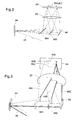
- Figs 2 and 3 illustrate a first embodiment of the invention. Only the analyser and detector parts of the system are shown.
- the optical components for illuminating the sample and collecting scattered light may be as shown in Fig 1, or any other conventional arrangement.
- the system of Figs 2 and 3 uses a CCD 24 as a detector and a diffraction grating 44 which acts to disperse the Raman scattered light of an incoming beam 36 as a spectrum horizontally across the width of the CCD 24.
- the grating 44 is arranged to disperse the spectrum of interest more widely than can be accommodated within the single width of the CCD 24.
- Edge filters 38A,38B and a mirror 46 are arranged in the path of the dispersed spectrum, between the diffraction grating 44 and the lens 22 which focuses the spectrum onto the CCD 24.
- the first filter 38A passes the medium and low wavenumbers, but reflects higher wavenumbers as a dispersed beam 48A. This is focused by the lens 22 to produce a spectrum at 50A on the CCD 24.
- the cut-off or edge of the edge filter 38B is arranged to be lower in wavenumbers than that of the filter 38A, so that light of the medium wavenumbers which has passed through the filter 38A is reflected by the filter 38B, as a beam 48B.
- the lens 22 focuses this beam onto the CCD as a spectrum 50B.
- light of the low wavenumbers which passes through both the filters 38A and 38B is reflected by the mirror 46 as a beam 48C, focused as a spectrum 50C on the CCD 24 by the lens 22.
- the filters 38A,38B and the mirror 46 are all tilted to different horizontal angles (i.e. tilted about their vertical axes), such that the spectra 50A,50B,50C are reflected to the same horizontal location on the CCD 24.
- the filters 38A,38B and mirror 46 are each given a slightly different tilt in the vertical direction (i.e. about their horizontal axes) so that the spectra 50A,50B,50C are separated from each other in the vertical direction on the CCD 24, as best seen in Fig 3. In this way, the whole spectrum of interest is focused simultaneously onto the CCD 24, in three separate parts, without loss of resolution.
- the data for the three parts of the spectrum is acquired from the CCD by the computer 25 (Fig 1), where software joins together the data for the separate parts so as to display or print out the complete spectrum.
- Some spectral information may be lost at the joins, but this loss is minimal provided the cut-off edges of the filters are sharp.
- the joins between the individual spectra 50A,50B and between the spectra 50B,50C can overlap, ideally with sharp cut-off edges, but more gradual cut-off edges can be accommodated.
- the software can correct the resulting data from a look-up table, derived by pre-calibrating the instrument by dispersing a known spectrum with the grating 44.
- Figs 2 and 3 has several advantages over prior art systems which rotate the grating 44 stepwise to disperse different parts of the spectrum across the CCD. First of all, the time required to acquire the data for the whole spectrum is reduced. There is also no need for the diffraction grating 44 to be mounted upon a precision rotatable stage, which as previously described would need to be indexed to carefully controlled positions. It is a significant advantage that the arrangement has no moving parts in use. Another advantage is that all the different parts of the spectrum 50A-50C are obtained simultaneously, under the same conditions, since this obviates the problems experienced with the previous method if conditions such as background light should change between the measurements on the different partial spectra.
- Figs 4 and 5 show an alternative to the arrangement of Figs 2 and 3.
- the filters 38A,38B and the mirror 46 are arranged before the diffraction grating 44.
- they are tilted so as to split the incoming beam 36 into three parts having different wavenumber ranges, which are then dispersed by the diffraction grating 44 into three partial spectra 50A,50B,50C which appear vertically above each other on the CCD 24.
- This arrangement has an advantage over that of Figs 3 and 4, in that the physical sizes of the filters 38A,38B and of the lens 22 can be smaller and these components can therefore be cheaper and more easily realised. In particular, the aberrations caused by the lens 22 can be reduced in this arrangement.
- Fig 6 shows a practical layout of a system in accordance with the principle shown in Figs 4 and 5.
- the various optical components shown in Fig 6 are all contained within a housing 60.
- An incoming laser beam 10 (which may be generated by a laser external to the housing 60) is reflected by a mirror 62 onto a dichroic notch filter 64, e.g. a holographic notch filter.
- This filter 64 reflects light of the frequency of the incoming laser beam, but transmits all other frequencies. It thus reflects the incoming laser beam 10 along a path 66, outside the housing 60, through suitable optics (not shown) to illuminate a sample.
- the Raman scattered light passes through conventional components indicated generally at 69. These may optionally include an entrance slit and associated lenses, a polarising filter for investigating the polarisation state of the Raman scattered light, an additional notch filter for rejecting Rayleigh scattered light, etc.
- the Raman scattered light passes to edge filters 38A,38B and a mirror 46, which function as described in relation to Figs 4 and 5 to split the Raman scattered light into different spectral regions and reflect the three partial spectral regions to a beam folding mirror 68, and thence to a diffraction grating 70.
- This disperses the three beams 48A-48C, and three resulting partial spectra are focused by a lens 22 onto a CCD 24.
- the filters 38A,38B and mirror 46 are tilted at different angles out of the plane of Fig 6 so that these three partial spectra are vertically displaced one above another on the CCD 24.
- the filters 38A,38B, mirror 46 and diffraction grating 70 should be adjusted to the correct positions and angles within the plane of Fig 6 (i.e. tilted to the correct angles about axes normal to the plane of Fig 6). These angles depend upon the desired angles of incidence of the three reflected beams upon the diffraction grating 70 and upon the resulting angles to which the desired three partial spectra will be dispersed by the diffraction grating so as to appear in the desired positions on the CCD 24. These angles can be calculated with reference to the wavelengths concerned, the pitch of the grating 70 etc.
- a particular feature of the arrangement shown in Fig 6 is that the design is readily adaptable for laser sources of different wavelengths.
- the arrangement With the mirror in the position designated 68, the arrangement is suitable for a laser source with a wavelength 633nm. This can readily be adapted to accommodate laser sources with wavelengths of (for example) 780nm or 1064nm.
- the adaptation involves moving the mirror to the positions designated 68' and 68" respectively; replacing the grating 70 with one of a different pitch and tilting it to an appropriate angle within the horizontal plane of Fig 6; choosing appropriate filters 38A,38B to suit the required wavelengths; and minor adjustments in the positions and angles of the filter 38A and mirror 46 (as indicated by broken lines and by the three alternative paths for the beams 48A and 48C).
- the silicon CCD 24 may not be sufficiently sensitive, so it could be replaced by (for example) a gallium arsenide 2D photodetector array.
- the tilting of the grating 70 to the correct angle may be achieved by mounting it on a pivoting stage 72.
- This stage 72 does not move in use and so does not need to be rotated to accurately indexed positions under automatic control. It can therefore be significantly cheaper than the precision rotary stage required in EP 0543578.
- the movement of the mirror 68 to the appropriate position may be achieved by the provision of alternative mounting fixtures at the three locations.
- the filters 38A,38B and 46 may be mounted on adjustable optical mounts 74, with screw adjustments for altering the position both translationally and by tilting about horizontal and vertical axes. Suitable adjustable mounts are available commercially from Photon Control Limited, Cambridge, United Kingdom or from Newport Corporation, Fountain Valley, California, U.S.A. Similar mounts may also be used for the mirror 62 and the holographic filter 64, and for mounting the diffraction grating 70 on the stage 72, although in these cases the full range of potential adjustment will not be required.
- the beam folding mirror 68 is not essential. However, in the Fig 6 arrangement, it produces two advantages. Firstly, it enables the various optical components to be fitted into a housing 60 of smaller size. Secondly, a simple change in the position of the mirror 68 accommodates a wide variety of included angles between the beams 48A-C and the centre line 76 of the spectra dispersed towards the CCD 24. As already mentioned, this wide variety of angles accommodates a wide variety of wavelengths for the laser source.
- Figs 2-6 have used reflection gratings for the diffraction grating 44.
- a reflection grating can have advantages where the optical components are to be fitted into a housing of small size, since the reflection produces a folding of the light beam.
- a transmission grating can be placed nearer to the lens 22 than is possible with a reflection grating, since there is no need to ensure that the incoming beam to the grating does not clash with the lens. Since the grating can be closer to the lens, it is possible to use a smaller, cheaper lens or one with less aberrations.
- Fig 7 shows another embodiment.
- the lens 22, CCD 24 and a transmission grating 44A lie generally in a plane which is tilted with respect to the incoming beam 36.
- the line of these components is tilted both above the line of the incoming beam and out of the plane of the paper.
- the filter 38B is arranged in line with the centre points of the grating 44A, lens 22 and CCD 24, it will be seen that the filter 38A lies below this tilted plane, whilst the mirror 46 lies above the tilted plane.
- FIG 7 shows the use of a transmission grating 44A, it is equally possible to use a reflection grating, whilst still arranging this grating and the lens 22 and CCD 24 to lie in a plane which is tilted with respect to the incoming beam 36.
- Figs 2-7 have shown the spectrum being split into three sections by the use of two filters and a mirror. However, it is of course possible to use just one filter in order to split the spectrum into two; or to use more filters to split the spectrum into four or even more parts.
- the actual cut-off frequencies for each filter will of course depend upon the particular application, including the width of the spectrum which it is desired to investigate, and the wavelength of the exciting light.
- Fig 8 shows a plan view of another apparatus.
- Raman scattered light from a sample passes through an entrance slit 80 and is collimated by a lens 82.
- the apparatus has four beam arms 48A,48B,48C,48D, covering different parts of the spectrum as previously.
- the first arm 48A comprises that part of the spectrum which is transmitted by an edge filter 38A.
- a beam folding mirror 68 reflects this beam arm 48A to a transmission diffraction grating 44A. This disperses the respective part of the spectrum, which is then focused by a lens 22 onto a CCD camera 24.
- the edge filter 38A reflects the rest of the spectrum towards a mirror 46B, which in turn reflects it towards an edge filter 38B.
- the edge filter 38B transmits the second beam arm 48B towards the beam folding mirror 68 and diffraction grating 44A, where again it is dispersed and the dispersed spectrum is focused by the lens 22 onto the CCD camera 24.
- the third beam arm 48C is produced by reflection from the edge filter 38B and from a mirror 46C towards an edge filter 38C, which transmits the light in the relevant part of the spectrum.
- the edge filter 38C reflects the part of the spectrum which makes up the fourth beam arm 48D towards a mirror 46D.
- Fig 9 is a schematic side view which shows how this is achieved, while still focusing the beam arms 48A-D vertically above each other on the CCD 24. For clarity, this side view has been shown unfolded, that is to say ignoring the beam folding mirror 68 and the angles of diffraction at the grating 44A.
- these filters and mirrors are also tilted as shown in Fig 9 in a vertical direction (i.e.
- each of the arms 48B-D is tilted slightly in the vertical direction out of the plane of Fig 8. After passing through the central region of the lens 22, therefore, the partial spectra formed from each of the arms 48A-D are spaced vertically one above the other on the CCD 24.
- the grating 44A, lens 22 and CCD 24 are also shown with a slight vertical tilt, in order that they remain symmetrical about the beam arms 48A-48D, thereby reducing abberations and making the best possible use of the available detector area of the CCD 24.
- these components should be in the same plane as the incoming beam 36. This is easily achieved by arranging the beam folding mirror 68 with a slight vertical tilt, thereby returning the grating 44A, lens 22 and CCD 24 to the required horizontal plane.
- the vertical tilt angles have been somewhat exaggerated in Fig 9. In practice, they are only of the order of one or a few degrees.
- the edge filters 38A-C and mirrors 46B-D are therefore only slightly out of the plane of the input beam 36, such that they are relatively easy to assemble in the required position on suitable adjustable mounts.
- the edge filters 38A-C each have a relatively low angle of incidence (about 10°) to the respective beam arm. Higher angles of incidence can be disadvantageous, since such filters can have transmission/reflection characteristics which are dependent on the polarisation state of the incident light. By keeping a low angle of incidence, such polarisation effects are minimised.
- filters 38A,38B,38C which pass lower wavenumbers and reflect higher wavenumbers (i.e. which pass shorter wavelengths and reflect longer wavelengths). It is of course possible to use an inverse arrangement, with filters which pass higher wavenumbers and reflect lower wavenumbers. Of course, rather than using edge filters as described, it is possible to use bandpass filters, and these may have advantages in giving greater rejection of the Rayleigh scattered light.
- the various lenses illustrated have been singlet lenses. However, in practice, singlet, doublet or compound lenses may be used, e.g. doublets with or without a meniscus lens, to achieve the required performance with low abberations.
- any of the described embodiments of the invention may use beam splitters in place of the filters 38A,38B,38C.
- the filters are preferred since at each pass through a beam splitter, 50% of the available light is lost. It can also be envisaged to use several separate diffraction gratings or other dispersive devices, each producing a respective one of the partial spectra in Figs 4-9.
- Figs 1 and 6 in which the incoming laser beam 10 is injected into the path 13 or 66 by the filter 12 or 64, is not essential. It is possible to illuminate the sample via an entirely separate optical path if desired.
- the invention can be used with spectroscopic apparatus having a remote, hand-held probe head, laser light being delivered to the probe head via a first optical fibre, and Raman scattered light being brought back along the path 66 by another optical fibre.
- Raman spectroscopy Although all the above examples have discussed Raman spectroscopy, the invention can of course be used in many other types of spectroscopy, including fluorescence, infra-red, narrow line photoluminescence, cathodoluminescence, etc.
Landscapes
- Physics & Mathematics (AREA)
- Spectroscopy & Molecular Physics (AREA)
- General Physics & Mathematics (AREA)
- Investigating, Analyzing Materials By Fluorescence Or Luminescence (AREA)
- Spectrometry And Color Measurement (AREA)
- Investigating Or Analysing Materials By Optical Means (AREA)
Description
Claims (11)
- Spectroscopic analysis apparatus comprising:characterised in that the detector (24) is two-dimensional, extending in a second direction perpendicular to the first direction; and wherein the light in a first part of the spectrum (50A) reaching the detector by a first one of said optical paths is spaced in said second direction from light in a second part of the spectrum (50B) reaching the detector by a second one of said optical paths.an optical input (36,66,80) for receiving a spectrum of scattered light produced from a sample;a detector (24) for the scattered light, extending in at least a first direction;a dispersive device (44,70,44A) arranged between the optical input and the detector to disperse a part of said spectrum across the detector in said first direction; andat least one light splitter (38A-C) arranged between the optical input and the detector to split the scattered light to follow at least two different optical paths (48A-D) to the detector, the light reaching the detector by each of the optical paths being filtered by a filter separate from said dispersive device so as to be in different parts of said spectrum;
- Apparatus according to claim 1, wherein there are at least three different optical paths (48A-D), and light in at least three parts of said spectrum reaches the detector via respective ones of said optical paths, at respective locations (50A-C) on said detector which are spaced apart in said second direction.
- Apparatus according to claim 1 or claim 2, wherein the detector (24) is a charge-coupled device.
- Apparatus according to any one of the preceding claims, wherein the light splitter (38A-C) is a filter which transmits one part of the spectrum along one optical path, and reflects another part of the spectrum along another optical path.
- Apparatus according to claim 4, wherein said filter (38A-C) is an edge filter.
- Apparatus according to claim 4 or claim 5 including a plurality of said filters (38A-C) for splitting the light into a plurality of said optical paths.
- Apparatus according to anyone of the preceding claims, wherein the light splitter or splitters (38A-C) lies between the optical input and the dispersive device.
- Apparatus according to any one of claims 1 to 6, wherein the light splitter or splitters (38A,38B) lies between the dispersive device and the detector.
- Apparatus according to any one of the preceding claims, including a common lens (22) for focusing the light in each of said optical paths onto the detector, each optical path passing through the centre of the lens.
- Apparatus according to any one of the preceding claims, wherein the dispersive device (44,70) and the detector (24) are generally co-planar with light received through the optical input.
- Apparatus according to any one of the preceding claims, wherein said spectrum which is detected is a spectrum of Raman scattered light.
Applications Claiming Priority (3)
| Application Number | Priority Date | Filing Date | Title |
|---|---|---|---|
| GB9410395A GB9410395D0 (en) | 1994-05-24 | 1994-05-24 | Spectroscopic apparatus |
| GB9410395 | 1994-05-24 | ||
| PCT/GB1995/001190 WO1995032408A1 (en) | 1994-05-24 | 1995-05-24 | Spectroscopic apparatus |
Publications (2)
| Publication Number | Publication Date |
|---|---|
| EP0711408A1 EP0711408A1 (en) | 1996-05-15 |
| EP0711408B1 true EP0711408B1 (en) | 2000-01-12 |
Family
ID=10755636
Family Applications (1)
| Application Number | Title | Priority Date | Filing Date |
|---|---|---|---|
| EP95919558A Expired - Lifetime EP0711408B1 (en) | 1994-05-24 | 1995-05-24 | Spectroscopic apparatus |
Country Status (9)
| Country | Link |
|---|---|
| US (1) | US5638173A (en) |
| EP (1) | EP0711408B1 (en) |
| JP (1) | JP3660680B2 (en) |
| KR (1) | KR960704216A (en) |
| DE (1) | DE69514485T2 (en) |
| GB (1) | GB9410395D0 (en) |
| TW (1) | TW324059B (en) |
| WO (1) | WO1995032408A1 (en) |
| ZA (1) | ZA954234B (en) |
Cited By (1)
| Publication number | Priority date | Publication date | Assignee | Title |
|---|---|---|---|---|
| CN106796143A (en) * | 2014-08-28 | 2017-05-31 | 瑞尼斯豪公司 | Spectroscopy equipment |
Families Citing this family (43)
| Publication number | Priority date | Publication date | Assignee | Title |
|---|---|---|---|---|
| JP3367545B2 (en) * | 1995-09-22 | 2003-01-14 | 株式会社ニコン | Optical spectrum detector |
| JPH09145477A (en) * | 1995-11-20 | 1997-06-06 | Tokyo Instr:Kk | Spectroscope |
| DE19735205A1 (en) * | 1997-08-14 | 1999-02-25 | Gustav Prof Dr Techn Schweiger | Spectroscopic determination of soot in the environment |
| DE19902625A1 (en) * | 1998-01-28 | 1999-09-30 | Leica Microsystems | Device for simultaneous detection of several spectral ranges of a light beam, such as that used with a laser scanner |
| US6885445B2 (en) | 1998-05-09 | 2005-04-26 | Renishaw Plc | Electron microscope and spectroscopy system |
| EP0995086B1 (en) * | 1998-05-09 | 2007-11-14 | Renishaw plc | Electron microscope and spectroscopy system |
| US6337472B1 (en) * | 1998-10-19 | 2002-01-08 | The University Of Texas System Board Of Regents | Light imaging microscope having spatially resolved images |
| JP2000283960A (en) * | 1999-03-31 | 2000-10-13 | Shimadzu Corp | Microchip electrophoresis device |
| US6351306B1 (en) | 1999-10-19 | 2002-02-26 | Kaiser Optical Systems, Inc. | Optical measurement probe calibration configurations |
| US6690467B1 (en) | 2000-05-05 | 2004-02-10 | Pe Corporation | Optical system and method for optically analyzing light from a sample |
| US6967717B1 (en) * | 2000-06-14 | 2005-11-22 | The United States Of America As Represented By The Secretary Of The Navy | Thermo-electrically cooled surface enhanced Raman spectroscopy sensor system |
| US6958811B2 (en) | 2000-06-29 | 2005-10-25 | Carl Zeiss Jena Gmbh | Method for the detection of dyes in fluorescence microscopy |
| US6747737B2 (en) | 2000-06-29 | 2004-06-08 | Carl Zeiss Jena Gmbh | Method for optical detection of an illuminated specimen in a plurality of detection channels |
| US6947133B2 (en) * | 2000-08-08 | 2005-09-20 | Carl Zeiss Jena Gmbh | Method for increasing the spectral and spatial resolution of detectors |
| US6858852B2 (en) | 2000-08-08 | 2005-02-22 | Carl Zeiss Jena Gmbh | Method and apparatus for rapid change of fluorescence bands in the detection of dyes in fluorescence microscopy |
| US6670087B2 (en) * | 2000-11-07 | 2003-12-30 | Canon Kabushiki Kaisha | Toner, image-forming apparatus, process cartridge and image forming method |
| JP2003121361A (en) * | 2001-10-11 | 2003-04-23 | Mitsubishi Heavy Ind Ltd | Method and apparatus for measuring micro constituent using laser beam |
| US6788407B1 (en) | 2002-03-18 | 2004-09-07 | Itt Manufacturing Enterprises, Inc. | Laser interrogation of surface agents |
| US20050182328A1 (en) * | 2002-08-09 | 2005-08-18 | Hamamatsu Photonics K.K. | System enabling chromaticity measurement in the visible and invisible ranges |
| DE102004026373B4 (en) * | 2004-05-29 | 2008-04-17 | Eads Astrium Gmbh | Method and device for detecting optical spectra |
| US7667882B2 (en) * | 2004-10-12 | 2010-02-23 | Georgia Tech Research Corp. | Fourier transform volume holographic spectrometer |
| US7616303B2 (en) * | 2005-04-25 | 2009-11-10 | University Of Massachusetts | Systems and methods for correcting optical reflectance measurements |
| JP4642621B2 (en) * | 2005-09-29 | 2011-03-02 | 株式会社フォトンデザイン | Spectrometer |
| US7564547B2 (en) * | 2005-11-07 | 2009-07-21 | Wafermasters, Inc. | Spectroscopy system |
| US7397561B2 (en) * | 2005-11-07 | 2008-07-08 | Wafermasters, Incorporated | Spectroscopy system |
| IL173025A0 (en) * | 2006-01-09 | 2007-03-08 | Oren Aharon | A method and apparatus for high resolution spectroscopy |
| US20080010019A1 (en) * | 2006-07-06 | 2008-01-10 | Thomas Richard A | High speed spectrum analyzer |
| DE102006047913B4 (en) * | 2006-10-06 | 2013-08-08 | Carl Zeiss Microscopy Gmbh | Highly sensitive spectral analytical unit |
| WO2008054908A2 (en) * | 2006-10-30 | 2008-05-08 | Georgia Tech Research Corporation | Tandem fabry-perot etalon cylindrical beam volume hologram for high resolution/large spectral range diffuse light spectroscopy |
| US8077309B2 (en) | 2007-01-29 | 2011-12-13 | Applied Instrument Technologies, Inc. | Chemical analyzer for industrial process control |
| JP2010169493A (en) * | 2009-01-22 | 2010-08-05 | National Institute Of Advanced Industrial Science & Technology | Spectroradiometer |
| US8922768B2 (en) * | 2010-10-04 | 2014-12-30 | Wasatch Photonics, Inc. | Multi-path spectrometer |
| FR2969282B1 (en) * | 2010-12-21 | 2014-07-18 | Horiba Jobin Yvon Sas | DEVICE AND METHOD FOR VISUALIZING AND MEASURING RAMAN DIFFUSION |
| JP5787151B2 (en) * | 2011-08-26 | 2015-09-30 | 株式会社ニコン | Spectroscopic unit and scanning microscope |
| US8334975B1 (en) * | 2011-09-26 | 2012-12-18 | Raytheon Company | Integrated 3-channel gas detection and measurement spectrometer |
| JP6311267B2 (en) * | 2013-05-10 | 2018-04-18 | 株式会社リコー | Spectral characteristic acquisition device, image evaluation device, image forming device |
| JP6248577B2 (en) * | 2013-11-26 | 2017-12-20 | 日本電気株式会社 | Slit width changing device and method and spectrum output device |
| US20150346102A1 (en) * | 2014-06-03 | 2015-12-03 | Innovative Photonic Solutions, Inc. | Compact Raman Probe Integrated with Wavelength Stabilized Diode Laser Source |
| DE112014007080B4 (en) * | 2014-12-22 | 2021-09-09 | Spectro Analytical Instruments Gmbh | Grating spectrometer with switchable light path |
| WO2017184109A1 (en) * | 2016-04-18 | 2017-10-26 | Hewlett-Packard Development Company, L.P. | Simultaneous detection of multiple spectra of scattered radiation |
| WO2020174239A1 (en) | 2019-02-27 | 2020-09-03 | Renishaw Plc | Spectroscopic apparatus |
| US11280675B2 (en) * | 2019-06-18 | 2022-03-22 | Ruolin Li | Method, system and apparatus for a Raman spectroscopic measurement system |
| JP2022071291A (en) | 2020-10-28 | 2022-05-16 | キヤノン株式会社 | Identification device |
Family Cites Families (16)
| Publication number | Priority date | Publication date | Assignee | Title |
|---|---|---|---|---|
| BE571401A (en) * | ||||
| US2453164A (en) * | 1945-05-19 | 1948-11-09 | Lane Wells Co | Plural grating spectrograph |
| FR2142059B3 (en) * | 1971-06-18 | 1975-08-08 | Johansson Axel | |
| US3733131A (en) * | 1971-08-05 | 1973-05-15 | Perkin Elmer Ltd | Optical beam switching devices utilizing a pair of plane mirrors |
| JPS57111422A (en) * | 1980-12-29 | 1982-07-10 | Shimadzu Corp | Spectrum measuring device |
| US4599001A (en) * | 1984-05-02 | 1986-07-08 | The United States Of America As Represented By The Administrator Of The National Aeronautics And Space Administration | Multispectral linear array multiband selection device |
| US4729658A (en) * | 1986-06-05 | 1988-03-08 | The Perkin-Elmer Corporation | Very wide spectral coverage grating spectrometer |
| US4747688A (en) * | 1986-09-26 | 1988-05-31 | The United States Of America As Represented By The Secretary Of The Air Force | Fiber optic coherence meter |
| GB8715949D0 (en) * | 1987-07-07 | 1987-08-12 | Beckman Riic Ltd | Spectrophotometers |
| GB2256923B (en) * | 1990-02-02 | 1993-09-22 | De La Rue Thomas & Co Ltd | Detection apparatus |
| WO1992017806A1 (en) * | 1991-04-05 | 1992-10-15 | Meridian Instruments, Inc. | Multiple path scanning microscope |
| EP0543578B1 (en) * | 1991-11-16 | 1995-06-28 | RENISHAW plc | Spectroscopic apparatus and methods |
| FI90289C (en) * | 1992-04-08 | 1994-01-10 | Valtion Teknillinen | Optical component |
| DE4223212C2 (en) * | 1992-07-15 | 1999-03-18 | Bodenseewerk Perkin Elmer Co | Grid polychromator |
| US5442439A (en) * | 1993-04-21 | 1995-08-15 | Kaiser Optical Systems, Inc. | Spectrograph with multiplexing of different wavelength regions onto a single opto-electric detector array |
| US5424826A (en) * | 1993-07-30 | 1995-06-13 | Control Development, Inc. | Wideband optical micro-spectrometer system |
-
1994
- 1994-05-24 GB GB9410395A patent/GB9410395D0/en active Pending
-
1995
- 1995-05-24 ZA ZA954234A patent/ZA954234B/en unknown
- 1995-05-24 DE DE69514485T patent/DE69514485T2/en not_active Expired - Lifetime
- 1995-05-24 KR KR1019960700310A patent/KR960704216A/en not_active Withdrawn
- 1995-05-24 JP JP53015795A patent/JP3660680B2/en not_active Expired - Fee Related
- 1995-05-24 WO PCT/GB1995/001190 patent/WO1995032408A1/en not_active Ceased
- 1995-05-24 EP EP95919558A patent/EP0711408B1/en not_active Expired - Lifetime
- 1995-05-24 US US08/578,651 patent/US5638173A/en not_active Expired - Lifetime
- 1995-06-09 TW TW084105893A patent/TW324059B/en active
Cited By (2)
| Publication number | Priority date | Publication date | Assignee | Title |
|---|---|---|---|---|
| CN106796143A (en) * | 2014-08-28 | 2017-05-31 | 瑞尼斯豪公司 | Spectroscopy equipment |
| CN106796143B (en) * | 2014-08-28 | 2019-04-23 | 瑞尼斯豪公司 | Spectroscopy equipment and spectroscopy methods |
Also Published As
| Publication number | Publication date |
|---|---|
| EP0711408A1 (en) | 1996-05-15 |
| US5638173A (en) | 1997-06-10 |
| JP3660680B2 (en) | 2005-06-15 |
| KR960704216A (en) | 1996-08-31 |
| GB9410395D0 (en) | 1994-07-13 |
| DE69514485D1 (en) | 2000-02-17 |
| ZA954234B (en) | 1996-01-22 |
| JPH09500970A (en) | 1997-01-28 |
| DE69514485T2 (en) | 2000-08-24 |
| WO1995032408A1 (en) | 1995-11-30 |
| TW324059B (en) | 1998-01-01 |
Similar Documents
| Publication | Publication Date | Title |
|---|---|---|
| US5638173A (en) | Spectrum splitting spectroscopic apparatus | |
| US5689333A (en) | Spectroscopic apparatus and methods | |
| JP2733491B2 (en) | Raman analyzer | |
| JP2834954B2 (en) | Spectrometer | |
| US5623342A (en) | Raman microscope | |
| US5841139A (en) | Optical instrument providing combined infrared and Ramen analysis of samples | |
| KR102347059B1 (en) | Overlay metrology using multiple parameter configurations | |
| DE69415641T2 (en) | Device for measuring thin film thickness | |
| US7102746B2 (en) | Raman spectroscope | |
| US6072624A (en) | Apparatus and method for scanning laser imaging of macroscopic samples | |
| EP1983332B1 (en) | A spectroscopic imaging method and system for exploring the surface of a sample | |
| JP2831124B2 (en) | Spectroscopic microscope with one photometer | |
| US10067058B1 (en) | Auto-focus system | |
| US7230697B2 (en) | Method and apparatus for multi-mode spectral imaging | |
| JP6811708B2 (en) | Spectrometer | |
| CN117405646A (en) | Raman spectroscopy equipment and methods | |
| US6414753B1 (en) | Low stray light czerny-turner monochromator | |
| WO2025027314A2 (en) | An optical mount and spectrometer comprising the optical mount | |
| WO2020174239A1 (en) | Spectroscopic apparatus | |
| EP4680923A1 (en) | Spectroscopy apparatus and methods | |
| CA2090483A1 (en) | Fabrication of multifunctional holographic optical elements and application in photometers | |
| JPH10253450A (en) | Filter spectrometer |
Legal Events
| Date | Code | Title | Description |
|---|---|---|---|
| PUAI | Public reference made under article 153(3) epc to a published international application that has entered the european phase |
Free format text: ORIGINAL CODE: 0009012 |
|
| 17P | Request for examination filed |
Effective date: 19960116 |
|
| AK | Designated contracting states |
Kind code of ref document: A1 Designated state(s): CH DE FR GB IT LI NL |
|
| 17Q | First examination report despatched |
Effective date: 19971113 |
|
| GRAG | Despatch of communication of intention to grant |
Free format text: ORIGINAL CODE: EPIDOS AGRA |
|
| GRAG | Despatch of communication of intention to grant |
Free format text: ORIGINAL CODE: EPIDOS AGRA |
|
| GRAH | Despatch of communication of intention to grant a patent |
Free format text: ORIGINAL CODE: EPIDOS IGRA |
|
| GRAH | Despatch of communication of intention to grant a patent |
Free format text: ORIGINAL CODE: EPIDOS IGRA |
|
| GRAA | (expected) grant |
Free format text: ORIGINAL CODE: 0009210 |
|
| ITF | It: translation for a ep patent filed | ||
| AK | Designated contracting states |
Kind code of ref document: B1 Designated state(s): CH DE FR GB IT LI NL |
|
| REG | Reference to a national code |
Ref country code: CH Ref legal event code: NV Representative=s name: KIRKER & CIE SA Ref country code: CH Ref legal event code: EP |
|
| REF | Corresponds to: |
Ref document number: 69514485 Country of ref document: DE Date of ref document: 20000217 |
|
| ET | Fr: translation filed | ||
| PGFP | Annual fee paid to national office [announced via postgrant information from national office to epo] |
Ref country code: CH Payment date: 20000417 Year of fee payment: 6 |
|
| PGFP | Annual fee paid to national office [announced via postgrant information from national office to epo] |
Ref country code: NL Payment date: 20000425 Year of fee payment: 6 |
|
| PLBE | No opposition filed within time limit |
Free format text: ORIGINAL CODE: 0009261 |
|
| STAA | Information on the status of an ep patent application or granted ep patent |
Free format text: STATUS: NO OPPOSITION FILED WITHIN TIME LIMIT |
|
| 26N | No opposition filed | ||
| PG25 | Lapsed in a contracting state [announced via postgrant information from national office to epo] |
Ref country code: LI Free format text: LAPSE BECAUSE OF NON-PAYMENT OF DUE FEES Effective date: 20010623 Ref country code: CH Free format text: LAPSE BECAUSE OF NON-PAYMENT OF DUE FEES Effective date: 20010623 |
|
| PG25 | Lapsed in a contracting state [announced via postgrant information from national office to epo] |
Ref country code: NL Free format text: LAPSE BECAUSE OF NON-PAYMENT OF DUE FEES Effective date: 20011201 |
|
| REG | Reference to a national code |
Ref country code: GB Ref legal event code: IF02 |
|
| REG | Reference to a national code |
Ref country code: CH Ref legal event code: PL |
|
| NLV4 | Nl: lapsed or anulled due to non-payment of the annual fee |
Effective date: 20011201 |
|
| PG25 | Lapsed in a contracting state [announced via postgrant information from national office to epo] |
Ref country code: IT Free format text: LAPSE BECAUSE OF NON-PAYMENT OF DUE FEES Effective date: 20050524 |
|
| PGFP | Annual fee paid to national office [announced via postgrant information from national office to epo] |
Ref country code: DE Payment date: 20130522 Year of fee payment: 19 Ref country code: GB Payment date: 20130521 Year of fee payment: 19 |
|
| PGFP | Annual fee paid to national office [announced via postgrant information from national office to epo] |
Ref country code: FR Payment date: 20130603 Year of fee payment: 19 |
|
| REG | Reference to a national code |
Ref country code: DE Ref legal event code: R119 Ref document number: 69514485 Country of ref document: DE |
|
| GBPC | Gb: european patent ceased through non-payment of renewal fee |
Effective date: 20140524 |
|
| REG | Reference to a national code |
Ref country code: DE Ref legal event code: R119 Ref document number: 69514485 Country of ref document: DE Effective date: 20141202 |
|
| REG | Reference to a national code |
Ref country code: FR Ref legal event code: ST Effective date: 20150130 |
|
| PG25 | Lapsed in a contracting state [announced via postgrant information from national office to epo] |
Ref country code: DE Free format text: LAPSE BECAUSE OF NON-PAYMENT OF DUE FEES Effective date: 20141202 |
|
| PG25 | Lapsed in a contracting state [announced via postgrant information from national office to epo] |
Ref country code: FR Free format text: LAPSE BECAUSE OF NON-PAYMENT OF DUE FEES Effective date: 20140602 Ref country code: GB Free format text: LAPSE BECAUSE OF NON-PAYMENT OF DUE FEES Effective date: 20140524 |