EP0710992B1 - Superconducting metal oxide film and method of preparing same - Google Patents
Superconducting metal oxide film and method of preparing same Download PDFInfo
- Publication number
- EP0710992B1 EP0710992B1 EP95307930A EP95307930A EP0710992B1 EP 0710992 B1 EP0710992 B1 EP 0710992B1 EP 95307930 A EP95307930 A EP 95307930A EP 95307930 A EP95307930 A EP 95307930A EP 0710992 B1 EP0710992 B1 EP 0710992B1
- Authority
- EP
- European Patent Office
- Prior art keywords
- substrate
- superconducting film
- superconducting
- temperature
- oxygen
- Prior art date
- Legal status (The legal status is an assumption and is not a legal conclusion. Google has not performed a legal analysis and makes no representation as to the accuracy of the status listed.)
- Expired - Lifetime
Links
- 238000000034 method Methods 0.000 title claims description 16
- 229910044991 metal oxide Inorganic materials 0.000 title description 4
- 150000004706 metal oxides Chemical class 0.000 title description 4
- 239000000758 substrate Substances 0.000 claims description 25
- QVGXLLKOCUKJST-UHFFFAOYSA-N atomic oxygen Chemical compound [O] QVGXLLKOCUKJST-UHFFFAOYSA-N 0.000 claims description 21
- 239000001301 oxygen Substances 0.000 claims description 21
- 229910052760 oxygen Inorganic materials 0.000 claims description 21
- XKRFYHLGVUSROY-UHFFFAOYSA-N Argon Chemical compound [Ar] XKRFYHLGVUSROY-UHFFFAOYSA-N 0.000 claims description 16
- 239000013078 crystal Substances 0.000 claims description 13
- 238000000151 deposition Methods 0.000 claims description 11
- 230000008021 deposition Effects 0.000 claims description 10
- 229910052786 argon Inorganic materials 0.000 claims description 8
- 238000004544 sputter deposition Methods 0.000 claims description 8
- 229910002370 SrTiO3 Inorganic materials 0.000 claims description 5
- 229910021521 yttrium barium copper oxide Inorganic materials 0.000 claims description 5
- 229910003200 NdGaO3 Inorganic materials 0.000 claims description 4
- CPLXHLVBOLITMK-UHFFFAOYSA-N magnesium oxide Inorganic materials [Mg]=O CPLXHLVBOLITMK-UHFFFAOYSA-N 0.000 claims description 4
- 238000002360 preparation method Methods 0.000 claims description 4
- 238000004549 pulsed laser deposition Methods 0.000 claims description 4
- 239000010408 film Substances 0.000 description 42
- 238000002441 X-ray diffraction Methods 0.000 description 5
- 239000002887 superconductor Substances 0.000 description 5
- IJGRMHOSHXDMSA-UHFFFAOYSA-N Atomic nitrogen Chemical compound N#N IJGRMHOSHXDMSA-UHFFFAOYSA-N 0.000 description 4
- 239000000463 material Substances 0.000 description 3
- 238000001451 molecular beam epitaxy Methods 0.000 description 3
- 229910002244 LaAlO3 Inorganic materials 0.000 description 2
- 238000004458 analytical method Methods 0.000 description 2
- 239000007788 liquid Substances 0.000 description 2
- 238000007431 microscopic evaluation Methods 0.000 description 2
- 229910052757 nitrogen Inorganic materials 0.000 description 2
- 239000010409 thin film Substances 0.000 description 2
- 238000006243 chemical reaction Methods 0.000 description 1
- 229910052802 copper Inorganic materials 0.000 description 1
- 230000006866 deterioration Effects 0.000 description 1
- 239000007789 gas Substances 0.000 description 1
- 239000012535 impurity Substances 0.000 description 1
- 238000009616 inductively coupled plasma Methods 0.000 description 1
- 238000010128 melt processing Methods 0.000 description 1
- 230000001590 oxidative effect Effects 0.000 description 1
- 238000012856 packing Methods 0.000 description 1
- 230000005855 radiation Effects 0.000 description 1
- 229910052761 rare earth metal Inorganic materials 0.000 description 1
- 238000002128 reflection high energy electron diffraction Methods 0.000 description 1
- 238000004611 spectroscopical analysis Methods 0.000 description 1
- 238000001771 vacuum deposition Methods 0.000 description 1
- 238000007740 vapor deposition Methods 0.000 description 1
Images





Classifications
-
- H—ELECTRICITY
- H10—SEMICONDUCTOR DEVICES; ELECTRIC SOLID-STATE DEVICES NOT OTHERWISE PROVIDED FOR
- H10N—ELECTRIC SOLID-STATE DEVICES NOT OTHERWISE PROVIDED FOR
- H10N60/00—Superconducting devices
- H10N60/80—Constructional details
- H10N60/85—Superconducting active materials
- H10N60/855—Ceramic superconductors
- H10N60/857—Ceramic superconductors comprising copper oxide
-
- Y—GENERAL TAGGING OF NEW TECHNOLOGICAL DEVELOPMENTS; GENERAL TAGGING OF CROSS-SECTIONAL TECHNOLOGIES SPANNING OVER SEVERAL SECTIONS OF THE IPC; TECHNICAL SUBJECTS COVERED BY FORMER USPC CROSS-REFERENCE ART COLLECTIONS [XRACs] AND DIGESTS
- Y10—TECHNICAL SUBJECTS COVERED BY FORMER USPC
- Y10S—TECHNICAL SUBJECTS COVERED BY FORMER USPC CROSS-REFERENCE ART COLLECTIONS [XRACs] AND DIGESTS
- Y10S428/00—Stock material or miscellaneous articles
- Y10S428/922—Static electricity metal bleed-off metallic stock
- Y10S428/9265—Special properties
- Y10S428/93—Electric superconducting
-
- Y—GENERAL TAGGING OF NEW TECHNOLOGICAL DEVELOPMENTS; GENERAL TAGGING OF CROSS-SECTIONAL TECHNOLOGIES SPANNING OVER SEVERAL SECTIONS OF THE IPC; TECHNICAL SUBJECTS COVERED BY FORMER USPC CROSS-REFERENCE ART COLLECTIONS [XRACs] AND DIGESTS
- Y10—TECHNICAL SUBJECTS COVERED BY FORMER USPC
- Y10S—TECHNICAL SUBJECTS COVERED BY FORMER USPC CROSS-REFERENCE ART COLLECTIONS [XRACs] AND DIGESTS
- Y10S505/00—Superconductor technology: apparatus, material, process
- Y10S505/70—High TC, above 30 k, superconducting device, article, or structured stock
- Y10S505/701—Coated or thin film device, i.e. active or passive
Definitions
- This invention relates to a superconducting metal oxide film and a method of preparing same.
- REBa 2 Cu 3 O 7 (RE: Y or a rare earth element) metal oxide superconductors are known to have a common crystal structure and are generally termed 123 superconductor materials.
- a typical example of such a superconductor is YBa 2 Cu 3 O 7 .
- a bulk of NdBa 2 Cu 3 O 7-d prepared by an OCMG (oxygen controlled melt growth) method is known to exhibit an excellent critical current density (Jc characteristics) in a high molecular field.
- a superconducting film of NdBa 2 Cu 3 O 7-d prepared by an MBE (molecular beam epitaxy) method is disclosed in Appl. Phys. Lett.
- an object of the present invention to provide a superconducting metal oxide film which is composed of Nd, Ba, Cu and 0, which has a crystal structure similar to YBa 2 Cu 3 O 7 and which has a superconductive critical temperature Tc of higher than that of liquid nitrogen.
- a superconducting film having the same crystal structure as that of YBa 2 Cu 3 O 7 and the following composition: Nd 1+x Ba 2-x Cu 3 O 7-d wherein part of the Nd sites are occupied by Ba atoms and/or part of the Ba sites are occupied by Nd atoms, and wherein x and d are numbers satisfying the following conditions: 0.03 ⁇ x ⁇ 0.12 0 ⁇ d ⁇ 0.5.
- the superconducting film is formed on a substrate of a single crystal selected from SrTiO 3 , NdGaO 3 and MgO.
- the present invention also provides a further process for the preparation of the above preferred superconducting film, wherein said substrate is subjected to a high frequency sputtering using a sintered body of NdBa 2 Cu 3 O z where z is a number greater than 6 but not greater than 7 as a target while maintaining said substrate at a temperature of between 660°C and 760°C and in an atmosphere having a total pressure of argon and oxygen of between 50 mTorr and 140 mTorr and a volume ratio of argon to oxygen of between 1:1 and 4:1.
- the superconducting film according to the present invention has the same crystal structure as that of a 123 superconductor material, typically YBa 2 Cu 3 O 7 . Further, the total molar amounts of Nd and Ba of the superconducting film of the present invention relative to the amount of Cu is the same as that of NdBa 2 Cu 3 O 7 . However, the superconducting film of the present invention is clearly distinguished from the known NdBa 2 Cu 3 O 7 film in that Ba atoms are substituted for part of the Nd sites and/or Nd atoms are substituted for part of the Ba sites in the inventive superconducting film.
- composition of the superconducting film according to the present invention has the following composition: Nd 1+x Ba 2-x Cu 3 O 7-d wherein x and d are numbers satisfying the following conditions: 0.03 ⁇ x ⁇ 0.12 0 ⁇ d ⁇ 0.5.
- the superconducting film may be prepared by a pulsed laser deposition method or a high frequency sputtering method.
- a substrate of a single crystal such as SrTiO 3 , NdGaO 3 , LaAlO 3 or MgO is subjected to vacuum deposition using a sintered body of NdBa 2 Cu 3 O z (where z is a number greater than 6 but not greater than 7) as a target.
- the substrate is maintained at a temperature of between 650°C and 850°C and in an atmosphere having an oxygen pressure of between 6.65 N/m 2 and 39.9 N/m 2 (50-300 mTorr).
- a substrate of a single crystal such as SrTiO 3 , NdGaO 3 , LaAlO 3 or MgO is subjected to sputtering deposition using a sintered body of NdBa 2 Cu 3 O z (where z is a number greater than 6 but not greater than 7) as a target.
- the substrate is maintained at a temperature of between 660°C and 760°C and in an atmosphere having a total pressure of argon and oxygen of between 6.65 N/m 2 and 18.62 N/m 2 (50-140 mTorr) and a volume ratio of argon to oxygen of between 1:1 and 4:1.
- Tc superconducting critical temperature
- the superconducting film according to the present invention also has an advantage because the surface thereof is chemically stable. This characteristic is confirmed by good reproducibility of ⁇ -T curves (temperature dependency of specific resistance) as well as the spiral growth observed by AFM analysis (atomic force microscopic analysis).
- the surface grain density of the film is generally smaller than 10 5 /mm 2 .
- a substrate of a SrTiO 3 single crystal was disposed within a vapor deposition chamber together with a target.
- the target was a sintered body of NdBa 2 Cu 3 0 z (6 ⁇ z ⁇ 7) and disposed at a position spaced apart a distance of 5 cm from the substrate.
- the substrate was heated by radiation from a heater at a temperature of 650-850°C in an oxygen atmosphere having an oxygen pressure of 50-300 mTorr. The distance between the substrate and the heater was maintained at 3 mm.
- the target was irradiated with pulsed ArF eximer laser 5,000 times at 5 Hz so that a superconductive thin film was deposited on the surface of the substrate.
- the energy density of the ArF eximer laser at a position of the surface of the target was varied in the range of 2.0-4 J/cm 2 .
- the actuation of the heater was stopped and the substrate was allowed to spontaneously cooled.
- the above operation was repeated at various oxygen pressures of 50, 75, 100, 200 and 300 mTorr and at various temperatures.
- Each of the thus obtained superconducting film was measured for the crystallinity thereof by X-ray diffraction analysis, for the composition thereof by inductively coupled plasma spectroscopy and for the conductive characteristics thereof by a four-terminal method.
- Fig. 2 shows X-ray diffraction patterns of the above superconducting films obtained at a determined deposition temperature of 850°C.
- the crystallinity of the superconducting films is similar to that of the substrate and no impurity phases are observed.
- Fig. 3 shows a relationship between the c-axis length of the superconducting film and the preset deposition temperature at various oxygen pressures.
- the results of Fig. 3 indicates that the c-axis length depends not only on the deposition temperature but also on the oxygen pressure.
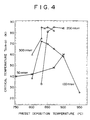
- the results shown in Fig. 4 indicate that the critical temperature Tc greatly depends on the oxygen pressure and that a high Tc is obtainable at an oxygen pressure of between 200-300 mTorr.
- Tc critical temperature
- Fig. 6 shows the temperature dependency of the electrical resistance of the superconducting film measured by a four-terminal method.
- Superconductivity starts at 91 K and the resistance is zero at 88 K. It was found that the temperature dependency of the electrical resistance was able to be measured with good reproducibility.
- An atomic force microscopic analysis (AFM) of the superconducting films revealed that the surface of the films was stable. Thus, when the superconducting films was allowed to stand in air for 2 weeks, no surface deterioration was observed and no change of the ⁇ -T characteristic curve was observed.
- AFM atomic force microscopic analysis
- a substrate of a MgO single crystal was disposed within a sputtering chamber together with a target.
- the target was a sintered body of NdBa 2 Cu 3 O z (6 ⁇ z ⁇ 7) and fixed to a Cu packing plate.
- the substrate was heated at a temperature of 660-760°C in an oxygen atmosphere having a total pressure of argon and oxygen of between 50 mTorr (5 x 1.333 Pa) and 140 mTorr (14 x 1.333 Pa) and a volume ratio of argon to oxygen of between 1:1 and 4:1.
- the target was sputtered using a high frequency wave of 13.65 MHz at 60 W so that a superconductive thin film was deposited on the surface of the substrate at a deposition rate of 4 nm/minute.
- the off-axis high frequency (RF) sputtering method is well known in the art and is disclosed in, for example, "Sputtering Technique" by Kiyotaka Sawa et al (edited by Kyoritsu Shuppan Inc. page 153 (1988).
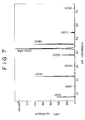
- Fig. 7 shows an X-ray diffraction pattern of the thus prepared superconducting film. This pattern suggests that the film is oriented in the direction of the c-axis.
- the analysis of the film by RHEED revealed streak patterns, suggesting that the crystal axis is oriented in the plane.
- Fig. 8 shows temperature dependency of the electrical resistance of the film, which was measured by the four-terminal method. The resistance became zero at the critical temperature Tc of 84 K. The conversion into the superconductive state occurred in a narrow temperature range. The intrinsic electrical resistance of the film was 10 -4 ⁇ cm.
Landscapes
- Chemical & Material Sciences (AREA)
- Engineering & Computer Science (AREA)
- Ceramic Engineering (AREA)
- Superconductor Devices And Manufacturing Methods Thereof (AREA)
- Superconductors And Manufacturing Methods Therefor (AREA)
- Inorganic Compounds Of Heavy Metals (AREA)
- Crystals, And After-Treatments Of Crystals (AREA)
- Physical Vapour Deposition (AREA)
- Containers, Films, And Cooling For Superconductive Devices (AREA)
Description
Claims (6)
- A superconducting film having the same crystal structure as that of YBa2Cu3O7 and the following composition:
- A superconducting film as claimed in Claim 1, having a superconducting critical temperature Tc of between 77K and 96K.
- A superconducting film as claimed in Claim 1 or Claim 2, having a c-axis length of greater that 1.170 nm (11.70 Å) but smaller than 1.177 nm (11.77 Å).
- A superconducting film as claimed in any preceding claim, formed on a substrate of a single crystal selected from SrTiO3, NdGaO3 and MgO.
- A process for the preparation of a superconducting film according to Claim 4, wherein said substrate is subjected to a pulsed laser deposition using a sintered body of NdBa2Cu3Oz where z is a number greater than 6 but not greater than 7 as a target while maintaining said substrate at a temperature of between 650°C and 850°C and in an atmosphere having an oxygen pressure of between 6.65 and 39.9 N/m2 (50-300 mTorr).
- A process for the preparation of a superconducting film according to Claim 4, wherein said substrate is subjected to a high frequency sputtering deposition using a sintered body of NdBa2Cu3Oz where z is a number greater than 6 but not greater than 7 as a target while maintaining said substrate at a temperature of between 660°C and 760°C and in an atmosphere having a total pressure of argon and oxygen of between 6.65 and 18.62 N/m2 (50-140 mTorr) and a volume ratio of argon to oxygen of between 1:1 and 4:1.
Applications Claiming Priority (2)
| Application Number | Priority Date | Filing Date | Title |
|---|---|---|---|
| JP272746/94 | 1994-11-07 | ||
| JP27274694A JP3207058B2 (en) | 1994-11-07 | 1994-11-07 | Superconductor thin film and method of manufacturing the same |
Publications (2)
| Publication Number | Publication Date |
|---|---|
| EP0710992A1 EP0710992A1 (en) | 1996-05-08 |
| EP0710992B1 true EP0710992B1 (en) | 1998-06-10 |
Family
ID=17518189
Family Applications (1)
| Application Number | Title | Priority Date | Filing Date |
|---|---|---|---|
| EP95307930A Expired - Lifetime EP0710992B1 (en) | 1994-11-07 | 1995-11-07 | Superconducting metal oxide film and method of preparing same |
Country Status (4)
| Country | Link |
|---|---|
| US (1) | US5650376A (en) |
| EP (1) | EP0710992B1 (en) |
| JP (1) | JP3207058B2 (en) |
| DE (1) | DE69502911T2 (en) |
Families Citing this family (29)
| Publication number | Priority date | Publication date | Assignee | Title |
|---|---|---|---|---|
| JP3962107B2 (en) * | 1996-03-22 | 2007-08-22 | 財団法人国際超電導産業技術研究センター | Oxide superconducting composite, method for producing the same, oxide superconducting magnet, and superconducting coil device |
| JP3392653B2 (en) * | 1996-09-02 | 2003-03-31 | 財団法人国際超電導産業技術研究センター | Oxide superconductor Josephson junction device and method of manufacturing the same |
| JP2000256012A (en) * | 1999-03-05 | 2000-09-19 | Internatl Superconductivity Technology Center | Oxide superconductor and manufacturing method thereof |
| JP2003059352A (en) * | 2001-08-22 | 2003-02-28 | Internatl Superconductivity Technology Center | High temperature superconductor film with flat surface |
| US6918213B2 (en) * | 2002-04-29 | 2005-07-19 | Stallion Fence Accessories | Plastic pergola end caps of extended length |
| US6690567B1 (en) | 2002-09-26 | 2004-02-10 | Ceramphysics, Inc. | Capacitive energy storage device |
| CN100564312C (en) * | 2004-12-23 | 2009-12-02 | 超导技术公司 | (RE)Ba2Cu3O7-δ thin-film superconductors with optimized compositions for RF properties |
| WO2007015569A1 (en) * | 2005-08-01 | 2007-02-08 | Eisai R & D Management Co., Ltd. | Method for prediction of the efficacy of vascularization inhibitor |
| EP1925676A4 (en) * | 2005-08-02 | 2010-11-10 | Eisai R&D Man Co Ltd | METHOD FOR ANALYZING THE EFFECT OF A VASCULARIZATION INHIBITOR |
| EP1938842A4 (en) * | 2005-09-01 | 2013-01-09 | Eisai R&D Man Co Ltd | Method for preparation of pharmaceutical composition having improved disintegradability |
| CN101316590B (en) | 2005-11-07 | 2011-08-03 | 卫材R&D管理有限公司 | combined use of angiogenesis inhibitor and c-kit kinase inhibitor |
| WO2007136103A1 (en) * | 2006-05-18 | 2007-11-29 | Eisai R & D Management Co., Ltd. | Antitumor agent for thyroid cancer |
| EP2044939A1 (en) * | 2006-06-29 | 2009-04-08 | Eisai R&D Management Co., Ltd. | Therapeutic agent for liver fibrosis |
| KR101472600B1 (en) * | 2006-08-28 | 2014-12-15 | 에자이 알앤드디 매니지먼트 가부시키가이샤 | Antitumor agent for undifferentiated gastric cancer |
| EP2119707B1 (en) * | 2007-01-29 | 2015-01-14 | Eisai R&D Management Co., Ltd. | Composition for treatment of undifferentiated-type of gastric cancer |
| CN101848895B (en) | 2007-11-09 | 2013-10-23 | 卫材R&D管理有限公司 | Combined use of angiogenesis inhibitory substance and antitumor platinum complex |
| US20100324087A1 (en) * | 2008-01-29 | 2010-12-23 | Eisai R&D Management Co., Ltd. | Combined use of angiogenesis inhibitor and taxane |
| CA2802644C (en) | 2010-06-25 | 2017-02-21 | Eisai R & D Management Co., Ltd. | Antitumor agent using compounds having kinase inhibitory effect in combination |
| EP2700403B1 (en) | 2011-04-18 | 2015-11-25 | Eisai R&D Management Co., Ltd. | Therapeutic agent for tumor |
| WO2012166899A2 (en) | 2011-06-03 | 2012-12-06 | Eisai R&D Management Co., Ltd. | Biomarkers for predicting and assessing responsiveness of thyroid and kidney cancer subjects to lenvatinib compounds |
| AU2013364953A1 (en) | 2012-12-21 | 2015-04-30 | Eisai R&D Management Co., Ltd. | Amorphous form of quinoline derivative, and method for producing same |
| CN105264380B (en) | 2013-05-14 | 2017-09-05 | 卫材R&D管理有限公司 | Biomarkers for predicting and evaluating responsiveness of endometrial cancer subjects to lenvatinib compounds |
| CA2957005C (en) | 2014-08-28 | 2021-10-12 | Eisai R&D Management Co., Ltd. | High-purity quinoline derivative and method for manufacturing same |
| SG11201706630UA (en) | 2015-02-25 | 2017-09-28 | Eisai R&D Man Co Ltd | Method for suppressing bitterness of quinoline derivative |
| WO2016140717A1 (en) | 2015-03-04 | 2016-09-09 | Merck Sharp & Dohme Corp. | Combination of a pd-1 antagonist and a vegfr/fgfr/ret tyrosine kinase inhibitor for treating cancer |
| BR112017027227B1 (en) | 2015-06-16 | 2023-12-12 | Eisai R&D Management Co., Ltd | ANTI-CANCER AGENT |
| JP6553726B2 (en) | 2015-08-20 | 2019-07-31 | エーザイ・アール・アンド・ディー・マネジメント株式会社 | Tumor therapeutic agent |
| US12303505B2 (en) | 2017-02-08 | 2025-05-20 | Eisai R&D Management Co., Ltd. | Tumor-treating pharmaceutical composition |
| BR112019023064A2 (en) | 2017-05-16 | 2020-06-09 | Eisai R&D Man Co Ltd | treatment of hepatocellular carcinoma |
Family Cites Families (3)
| Publication number | Priority date | Publication date | Assignee | Title |
|---|---|---|---|---|
| JPH01164728A (en) * | 1987-12-21 | 1989-06-28 | Nippon Telegr & Teleph Corp <Ntt> | Oxide superconducting material |
| JP2515930B2 (en) * | 1991-02-13 | 1996-07-10 | 株式会社日立製作所 | Superconducting element |
| US5149684A (en) * | 1991-04-09 | 1992-09-22 | General Atomics | Production of a superconductor powder having a narrow melting transition width using a controlled oxygen atmosphere |
-
1994
- 1994-11-07 JP JP27274694A patent/JP3207058B2/en not_active Expired - Fee Related
-
1995
- 1995-11-06 US US08/554,585 patent/US5650376A/en not_active Expired - Lifetime
- 1995-11-07 DE DE69502911T patent/DE69502911T2/en not_active Expired - Lifetime
- 1995-11-07 EP EP95307930A patent/EP0710992B1/en not_active Expired - Lifetime
Also Published As
| Publication number | Publication date |
|---|---|
| JP3207058B2 (en) | 2001-09-10 |
| DE69502911T2 (en) | 1998-10-22 |
| US5650376A (en) | 1997-07-22 |
| EP0710992A1 (en) | 1996-05-08 |
| DE69502911D1 (en) | 1998-07-16 |
| JPH08133896A (en) | 1996-05-28 |
Similar Documents
| Publication | Publication Date | Title |
|---|---|---|
| US5650376A (en) | (Nd, Ba)3 Cu3 O7-d superconductor film | |
| Lathrop et al. | Production of YBa2Cu3O7− y superconducting thin films in situ by high‐pressure reactive evaporation and rapid thermal annealing | |
| EP0406126B2 (en) | Substrate having a superconductor layer | |
| EP0284489B2 (en) | Process for depositing a superconducting thin film | |
| Yun et al. | Fabrication of c‐oriented HgBa2Ca2Cu3O8+ δ superconducting thin films | |
| Bäuerle | Laser-induced formation and surface processing of high-temperature superconductors | |
| US6074768A (en) | Process for forming the oxide superconductor thin film and laminate of the oxide superconductor thin films | |
| US5508255A (en) | Epitaxial thallium high temperature superconducting films formed via a nucleation layer | |
| EP0410868A2 (en) | Superconducting thin film of compound oxide and process for preparing the same | |
| US5130294A (en) | High temperature superconductor-calcium titanate structures | |
| EP0347335B1 (en) | A superconducting thin film and a process for depositing the same | |
| EP0357500B1 (en) | Process for preparing a bismuth-type superconducting thin film | |
| Ramesh et al. | Thin film Y Ba Cu O high Tc superconductors: structure-property relationships | |
| CA2043541C (en) | Process for preparing high-temperature superconducting thin films | |
| Asano et al. | Block-by-block deposition of BSCCO thin films by PLD method | |
| US5296455A (en) | Process for preparing superconductor of compound oxide of Bi-Sr-Ca-Cu system | |
| Tsuge et al. | In-situ low-temperature growth of YBa/sub 2/Cu/sub 3/O/sub 7-x/films by reactive coevaporation | |
| Attanasio et al. | Realization and Characterization of e-Beam Completely Evaporated BSCCO Thin Films | |
| US5260267A (en) | Method for forming a Bi-containing superconducting oxide film on a substrate with a buffer layer of Bi2 O3 | |
| Boyce et al. | In-situ growth of superconducting YBa2Cu3Oy films by pulsed laser deposition | |
| US5420103A (en) | A-axis superconductor on a yttrium oxide film | |
| Li et al. | Heteroepitaxial growth of MgO films by dual ion beam sputtering | |
| Young et al. | Substrate interdiffusion in Tl2Ba2CaCu2O8 thin films and its effects on microwave device performance | |
| Yamamoto et al. | Stabilization of High-Tc Phase in Sputtered BiPbSrCaCuO Films by Post Anneal | |
| Kampwirth et al. | In-situ growth of superconducting films of Bi-Sr-Ca-Cu-O using magnetron sputtering |
Legal Events
| Date | Code | Title | Description |
|---|---|---|---|
| PUAI | Public reference made under article 153(3) epc to a published international application that has entered the european phase |
Free format text: ORIGINAL CODE: 0009012 |
|
| AK | Designated contracting states |
Kind code of ref document: A1 Designated state(s): DE FR GB |
|
| 17P | Request for examination filed |
Effective date: 19960520 |
|
| 17Q | First examination report despatched |
Effective date: 19961112 |
|
| GRAG | Despatch of communication of intention to grant |
Free format text: ORIGINAL CODE: EPIDOS AGRA |
|
| GRAG | Despatch of communication of intention to grant |
Free format text: ORIGINAL CODE: EPIDOS AGRA |
|
| GRAG | Despatch of communication of intention to grant |
Free format text: ORIGINAL CODE: EPIDOS AGRA |
|
| GRAH | Despatch of communication of intention to grant a patent |
Free format text: ORIGINAL CODE: EPIDOS IGRA |
|
| GRAH | Despatch of communication of intention to grant a patent |
Free format text: ORIGINAL CODE: EPIDOS IGRA |
|
| GRAA | (expected) grant |
Free format text: ORIGINAL CODE: 0009210 |
|
| AK | Designated contracting states |
Kind code of ref document: B1 Designated state(s): DE FR GB |
|
| REF | Corresponds to: |
Ref document number: 69502911 Country of ref document: DE Date of ref document: 19980716 |
|
| ET | Fr: translation filed | ||
| PLBE | No opposition filed within time limit |
Free format text: ORIGINAL CODE: 0009261 |
|
| STAA | Information on the status of an ep patent application or granted ep patent |
Free format text: STATUS: NO OPPOSITION FILED WITHIN TIME LIMIT |
|
| 26N | No opposition filed | ||
| REG | Reference to a national code |
Ref country code: GB Ref legal event code: IF02 |
|
| REG | Reference to a national code |
Ref country code: GB Ref legal event code: 732E |
|
| REG | Reference to a national code |
Ref country code: FR Ref legal event code: TQ |
|
| PGFP | Annual fee paid to national office [announced via postgrant information from national office to epo] |
Ref country code: FR Payment date: 20121130 Year of fee payment: 18 Ref country code: DE Payment date: 20121031 Year of fee payment: 18 |
|
| PGFP | Annual fee paid to national office [announced via postgrant information from national office to epo] |
Ref country code: GB Payment date: 20121107 Year of fee payment: 18 |
|
| GBPC | Gb: european patent ceased through non-payment of renewal fee |
Effective date: 20131107 |
|
| REG | Reference to a national code |
Ref country code: FR Ref legal event code: ST Effective date: 20140731 |
|
| REG | Reference to a national code |
Ref country code: DE Ref legal event code: R119 Ref document number: 69502911 Country of ref document: DE Effective date: 20140603 |
|
| PG25 | Lapsed in a contracting state [announced via postgrant information from national office to epo] |
Ref country code: DE Free format text: LAPSE BECAUSE OF NON-PAYMENT OF DUE FEES Effective date: 20140603 |
|
| PG25 | Lapsed in a contracting state [announced via postgrant information from national office to epo] |
Ref country code: GB Free format text: LAPSE BECAUSE OF NON-PAYMENT OF DUE FEES Effective date: 20131107 Ref country code: FR Free format text: LAPSE BECAUSE OF NON-PAYMENT OF DUE FEES Effective date: 20131202 |