EP0406126B2 - Substrate having a superconductor layer - Google Patents
Substrate having a superconductor layer Download PDFInfo
- Publication number
- EP0406126B2 EP0406126B2 EP90401911A EP90401911A EP0406126B2 EP 0406126 B2 EP0406126 B2 EP 0406126B2 EP 90401911 A EP90401911 A EP 90401911A EP 90401911 A EP90401911 A EP 90401911A EP 0406126 B2 EP0406126 B2 EP 0406126B2
- Authority
- EP
- European Patent Office
- Prior art keywords
- substrate
- thin film
- superconducting
- compound oxide
- oxide
- Prior art date
- Legal status (The legal status is an assumption and is not a legal conclusion. Google has not performed a legal analysis and makes no representation as to the accuracy of the status listed.)
- Expired - Lifetime
Links
- 239000000758 substrate Substances 0.000 title claims description 56
- 239000002887 superconductor Substances 0.000 title description 21
- 239000010409 thin film Substances 0.000 claims description 60
- 150000001875 compounds Chemical class 0.000 claims description 45
- 239000013078 crystal Substances 0.000 claims description 36
- 239000010949 copper Substances 0.000 claims description 29
- 229910002370 SrTiO3 Inorganic materials 0.000 claims description 12
- 229910052802 copper Inorganic materials 0.000 claims description 10
- RYGMFSIKBFXOCR-UHFFFAOYSA-N Copper Chemical compound [Cu] RYGMFSIKBFXOCR-UHFFFAOYSA-N 0.000 claims description 8
- 229910052746 lanthanum Inorganic materials 0.000 claims description 7
- 229910052727 yttrium Inorganic materials 0.000 claims description 6
- 229910052692 Dysprosium Inorganic materials 0.000 claims description 3
- 229910052691 Erbium Inorganic materials 0.000 claims description 3
- 229910052693 Europium Inorganic materials 0.000 claims description 3
- 229910052688 Gadolinium Inorganic materials 0.000 claims description 3
- 229910052689 Holmium Inorganic materials 0.000 claims description 3
- 229910052765 Lutetium Inorganic materials 0.000 claims description 3
- 229910052779 Neodymium Inorganic materials 0.000 claims description 3
- 229910052772 Samarium Inorganic materials 0.000 claims description 3
- 229910052775 Thulium Inorganic materials 0.000 claims description 3
- 229910052769 Ytterbium Inorganic materials 0.000 claims description 3
- 229910052684 Cerium Inorganic materials 0.000 claims description 2
- 229910052777 Praseodymium Inorganic materials 0.000 claims description 2
- 229910052771 Terbium Inorganic materials 0.000 claims description 2
- 238000004544 sputter deposition Methods 0.000 description 14
- 239000010408 film Substances 0.000 description 12
- 229910021521 yttrium barium copper oxide Inorganic materials 0.000 description 11
- 230000000052 comparative effect Effects 0.000 description 10
- 229910002480 Cu-O Inorganic materials 0.000 description 9
- 239000007789 gas Substances 0.000 description 8
- 239000000203 mixture Substances 0.000 description 8
- 238000000034 method Methods 0.000 description 7
- QVGXLLKOCUKJST-UHFFFAOYSA-N atomic oxygen Chemical compound [O] QVGXLLKOCUKJST-UHFFFAOYSA-N 0.000 description 5
- 238000000151 deposition Methods 0.000 description 5
- 239000000463 material Substances 0.000 description 5
- 239000001301 oxygen Substances 0.000 description 5
- 229910052760 oxygen Inorganic materials 0.000 description 5
- 238000001771 vacuum deposition Methods 0.000 description 5
- 229910014454 Ca-Cu Inorganic materials 0.000 description 4
- 238000000137 annealing Methods 0.000 description 4
- 238000005229 chemical vapour deposition Methods 0.000 description 4
- 238000009792 diffusion process Methods 0.000 description 4
- 238000002003 electron diffraction Methods 0.000 description 4
- 238000005240 physical vapour deposition Methods 0.000 description 4
- 150000001621 bismuth Chemical class 0.000 description 3
- 238000001816 cooling Methods 0.000 description 3
- 238000010438 heat treatment Methods 0.000 description 3
- 230000006872 improvement Effects 0.000 description 3
- 238000007733 ion plating Methods 0.000 description 3
- 238000001451 molecular beam epitaxy Methods 0.000 description 3
- IJGRMHOSHXDMSA-UHFFFAOYSA-N Atomic nitrogen Chemical compound N#N IJGRMHOSHXDMSA-UHFFFAOYSA-N 0.000 description 2
- 229910001632 barium fluoride Inorganic materials 0.000 description 2
- 238000004519 manufacturing process Methods 0.000 description 2
- 230000005012 migration Effects 0.000 description 2
- 238000013508 migration Methods 0.000 description 2
- 125000004430 oxygen atom Chemical group O* 0.000 description 2
- 238000001552 radio frequency sputter deposition Methods 0.000 description 2
- 238000002128 reflection high energy electron diffraction Methods 0.000 description 2
- 229910001637 strontium fluoride Inorganic materials 0.000 description 2
- FVRNDBHWWSPNOM-UHFFFAOYSA-L strontium fluoride Chemical compound [F-].[F-].[Sr+2] FVRNDBHWWSPNOM-UHFFFAOYSA-L 0.000 description 2
- XUIMIQQOPSSXEZ-UHFFFAOYSA-N Silicon Chemical compound [Si] XUIMIQQOPSSXEZ-UHFFFAOYSA-N 0.000 description 1
- 229910003808 Sr-Cu Inorganic materials 0.000 description 1
- 229910003098 YBa2Cu3O7−x Inorganic materials 0.000 description 1
- 125000004429 atom Chemical group 0.000 description 1
- 230000015572 biosynthetic process Effects 0.000 description 1
- 229910052797 bismuth Inorganic materials 0.000 description 1
- JCXGWMGPZLAOME-UHFFFAOYSA-N bismuth atom Chemical compound [Bi] JCXGWMGPZLAOME-UHFFFAOYSA-N 0.000 description 1
- 230000008859 change Effects 0.000 description 1
- 238000007796 conventional method Methods 0.000 description 1
- 150000001879 copper Chemical class 0.000 description 1
- 230000006866 deterioration Effects 0.000 description 1
- 150000002222 fluorine compounds Chemical class 0.000 description 1
- 229910052747 lanthanoid Inorganic materials 0.000 description 1
- 150000002602 lanthanoids Chemical class 0.000 description 1
- 239000007788 liquid Substances 0.000 description 1
- CPLXHLVBOLITMK-UHFFFAOYSA-N magnesium oxide Inorganic materials [Mg]=O CPLXHLVBOLITMK-UHFFFAOYSA-N 0.000 description 1
- 230000015654 memory Effects 0.000 description 1
- 229910052751 metal Inorganic materials 0.000 description 1
- 229910052750 molybdenum Inorganic materials 0.000 description 1
- 229910052757 nitrogen Inorganic materials 0.000 description 1
- 239000000843 powder Substances 0.000 description 1
- 229910052710 silicon Inorganic materials 0.000 description 1
- 239000010703 silicon Substances 0.000 description 1
- 238000005245 sintering Methods 0.000 description 1
- 229910002076 stabilized zirconia Inorganic materials 0.000 description 1
- 229910052715 tantalum Inorganic materials 0.000 description 1
- 229910052721 tungsten Inorganic materials 0.000 description 1
- VWQVUPCCIRVNHF-UHFFFAOYSA-N yttrium atom Chemical compound [Y] VWQVUPCCIRVNHF-UHFFFAOYSA-N 0.000 description 1
Images
Classifications
-
- C—CHEMISTRY; METALLURGY
- C04—CEMENTS; CONCRETE; ARTIFICIAL STONE; CERAMICS; REFRACTORIES
- C04B—LIME, MAGNESIA; SLAG; CEMENTS; COMPOSITIONS THEREOF, e.g. MORTARS, CONCRETE OR LIKE BUILDING MATERIALS; ARTIFICIAL STONE; CERAMICS; REFRACTORIES; TREATMENT OF NATURAL STONE
- C04B41/00—After-treatment of mortars, concrete, artificial stone or ceramics; Treatment of natural stone
- C04B41/45—Coating or impregnating, e.g. injection in masonry, partial coating of green or fired ceramics, organic coating compositions for adhering together two concrete elements
- C04B41/52—Multiple coating or impregnating multiple coating or impregnating with the same composition or with compositions only differing in the concentration of the constituents, is classified as single coating or impregnation
-
- C—CHEMISTRY; METALLURGY
- C04—CEMENTS; CONCRETE; ARTIFICIAL STONE; CERAMICS; REFRACTORIES
- C04B—LIME, MAGNESIA; SLAG; CEMENTS; COMPOSITIONS THEREOF, e.g. MORTARS, CONCRETE OR LIKE BUILDING MATERIALS; ARTIFICIAL STONE; CERAMICS; REFRACTORIES; TREATMENT OF NATURAL STONE
- C04B41/00—After-treatment of mortars, concrete, artificial stone or ceramics; Treatment of natural stone
- C04B41/009—After-treatment of mortars, concrete, artificial stone or ceramics; Treatment of natural stone characterised by the material treated
-
- C—CHEMISTRY; METALLURGY
- C04—CEMENTS; CONCRETE; ARTIFICIAL STONE; CERAMICS; REFRACTORIES
- C04B—LIME, MAGNESIA; SLAG; CEMENTS; COMPOSITIONS THEREOF, e.g. MORTARS, CONCRETE OR LIKE BUILDING MATERIALS; ARTIFICIAL STONE; CERAMICS; REFRACTORIES; TREATMENT OF NATURAL STONE
- C04B41/00—After-treatment of mortars, concrete, artificial stone or ceramics; Treatment of natural stone
- C04B41/45—Coating or impregnating, e.g. injection in masonry, partial coating of green or fired ceramics, organic coating compositions for adhering together two concrete elements
- C04B41/50—Coating or impregnating, e.g. injection in masonry, partial coating of green or fired ceramics, organic coating compositions for adhering together two concrete elements with inorganic materials
- C04B41/5072—Coating or impregnating, e.g. injection in masonry, partial coating of green or fired ceramics, organic coating compositions for adhering together two concrete elements with inorganic materials with oxides or hydroxides not covered by C04B41/5025
- C04B41/5074—Copper oxide or solid solutions thereof
-
- C—CHEMISTRY; METALLURGY
- C04—CEMENTS; CONCRETE; ARTIFICIAL STONE; CERAMICS; REFRACTORIES
- C04B—LIME, MAGNESIA; SLAG; CEMENTS; COMPOSITIONS THEREOF, e.g. MORTARS, CONCRETE OR LIKE BUILDING MATERIALS; ARTIFICIAL STONE; CERAMICS; REFRACTORIES; TREATMENT OF NATURAL STONE
- C04B41/00—After-treatment of mortars, concrete, artificial stone or ceramics; Treatment of natural stone
- C04B41/80—After-treatment of mortars, concrete, artificial stone or ceramics; Treatment of natural stone of only ceramics
- C04B41/81—Coating or impregnation
- C04B41/85—Coating or impregnation with inorganic materials
-
- C—CHEMISTRY; METALLURGY
- C04—CEMENTS; CONCRETE; ARTIFICIAL STONE; CERAMICS; REFRACTORIES
- C04B—LIME, MAGNESIA; SLAG; CEMENTS; COMPOSITIONS THEREOF, e.g. MORTARS, CONCRETE OR LIKE BUILDING MATERIALS; ARTIFICIAL STONE; CERAMICS; REFRACTORIES; TREATMENT OF NATURAL STONE
- C04B41/00—After-treatment of mortars, concrete, artificial stone or ceramics; Treatment of natural stone
- C04B41/80—After-treatment of mortars, concrete, artificial stone or ceramics; Treatment of natural stone of only ceramics
- C04B41/81—Coating or impregnation
- C04B41/89—Coating or impregnation for obtaining at least two superposed coatings having different compositions
-
- C—CHEMISTRY; METALLURGY
- C30—CRYSTAL GROWTH
- C30B—SINGLE-CRYSTAL GROWTH; UNIDIRECTIONAL SOLIDIFICATION OF EUTECTIC MATERIAL OR UNIDIRECTIONAL DEMIXING OF EUTECTOID MATERIAL; REFINING BY ZONE-MELTING OF MATERIAL; PRODUCTION OF A HOMOGENEOUS POLYCRYSTALLINE MATERIAL WITH DEFINED STRUCTURE; SINGLE CRYSTALS OR HOMOGENEOUS POLYCRYSTALLINE MATERIAL WITH DEFINED STRUCTURE; AFTER-TREATMENT OF SINGLE CRYSTALS OR A HOMOGENEOUS POLYCRYSTALLINE MATERIAL WITH DEFINED STRUCTURE; APPARATUS THEREFOR
- C30B23/00—Single-crystal growth by condensing evaporated or sublimed materials
- C30B23/02—Epitaxial-layer growth
-
- C—CHEMISTRY; METALLURGY
- C30—CRYSTAL GROWTH
- C30B—SINGLE-CRYSTAL GROWTH; UNIDIRECTIONAL SOLIDIFICATION OF EUTECTIC MATERIAL OR UNIDIRECTIONAL DEMIXING OF EUTECTOID MATERIAL; REFINING BY ZONE-MELTING OF MATERIAL; PRODUCTION OF A HOMOGENEOUS POLYCRYSTALLINE MATERIAL WITH DEFINED STRUCTURE; SINGLE CRYSTALS OR HOMOGENEOUS POLYCRYSTALLINE MATERIAL WITH DEFINED STRUCTURE; AFTER-TREATMENT OF SINGLE CRYSTALS OR A HOMOGENEOUS POLYCRYSTALLINE MATERIAL WITH DEFINED STRUCTURE; APPARATUS THEREFOR
- C30B29/00—Single crystals or homogeneous polycrystalline material with defined structure characterised by the material or by their shape
- C30B29/10—Inorganic compounds or compositions
- C30B29/16—Oxides
- C30B29/22—Complex oxides
- C30B29/225—Complex oxides based on rare earth copper oxides, e.g. high T-superconductors
-
- H—ELECTRICITY
- H10—SEMICONDUCTOR DEVICES; ELECTRIC SOLID-STATE DEVICES NOT OTHERWISE PROVIDED FOR
- H10N—ELECTRIC SOLID-STATE DEVICES NOT OTHERWISE PROVIDED FOR
- H10N60/00—Superconducting devices
- H10N60/01—Manufacture or treatment
- H10N60/0268—Manufacture or treatment of devices comprising copper oxide
- H10N60/0296—Processes for depositing or forming copper oxide superconductor layers
- H10N60/0576—Processes for depositing or forming copper oxide superconductor layers characterised by the substrate
- H10N60/0632—Intermediate layers, e.g. for growth control
-
- C—CHEMISTRY; METALLURGY
- C04—CEMENTS; CONCRETE; ARTIFICIAL STONE; CERAMICS; REFRACTORIES
- C04B—LIME, MAGNESIA; SLAG; CEMENTS; COMPOSITIONS THEREOF, e.g. MORTARS, CONCRETE OR LIKE BUILDING MATERIALS; ARTIFICIAL STONE; CERAMICS; REFRACTORIES; TREATMENT OF NATURAL STONE
- C04B2111/00—Mortars, concrete or artificial stone or mixtures to prepare them, characterised by specific function, property or use
- C04B2111/00474—Uses not provided for elsewhere in C04B2111/00
- C04B2111/00844—Uses not provided for elsewhere in C04B2111/00 for electronic applications
-
- Y—GENERAL TAGGING OF NEW TECHNOLOGICAL DEVELOPMENTS; GENERAL TAGGING OF CROSS-SECTIONAL TECHNOLOGIES SPANNING OVER SEVERAL SECTIONS OF THE IPC; TECHNICAL SUBJECTS COVERED BY FORMER USPC CROSS-REFERENCE ART COLLECTIONS [XRACs] AND DIGESTS
- Y10—TECHNICAL SUBJECTS COVERED BY FORMER USPC
- Y10S—TECHNICAL SUBJECTS COVERED BY FORMER USPC CROSS-REFERENCE ART COLLECTIONS [XRACs] AND DIGESTS
- Y10S428/00—Stock material or miscellaneous articles
- Y10S428/922—Static electricity metal bleed-off metallic stock
- Y10S428/9265—Special properties
- Y10S428/93—Electric superconducting
-
- Y—GENERAL TAGGING OF NEW TECHNOLOGICAL DEVELOPMENTS; GENERAL TAGGING OF CROSS-SECTIONAL TECHNOLOGIES SPANNING OVER SEVERAL SECTIONS OF THE IPC; TECHNICAL SUBJECTS COVERED BY FORMER USPC CROSS-REFERENCE ART COLLECTIONS [XRACs] AND DIGESTS
- Y10—TECHNICAL SUBJECTS COVERED BY FORMER USPC
- Y10S—TECHNICAL SUBJECTS COVERED BY FORMER USPC CROSS-REFERENCE ART COLLECTIONS [XRACs] AND DIGESTS
- Y10S505/00—Superconductor technology: apparatus, material, process
- Y10S505/70—High TC, above 30 k, superconducting device, article, or structured stock
- Y10S505/701—Coated or thin film device, i.e. active or passive
Definitions
- the thin films of superconducting compound oxides prepared by vapour deposition techniques are subjected to after-treatment or post-annealing because their superconducting properties "as deposited" are poor. It is also known that the quality of the thin film is sharply deteriorated in the neighborhood of the substrate owing to diffusion of elements of which the substrate are composed during the post-annealing.
- U. S. patent No. 4,837,609 proposes to insert a layer of W, Mo or Ta between a superconducting compound oxide material and a silicon single crystal.
- a lattice plane of Cu-O composed of copper atoms and oxygen atoms is formed on a surface of the substrate on which the superconducting thin film of compound oxide is to be deposited by depositing an intermediate layer of compound oxide of copper having a crystal structure of perovskite type or layered perovskite type. Since the lattice plane of Cu-O has high crystalline matchability with the bismuth type compound oxide, the thin film of bismuth type compound oxide which is deposited on the intermediate layer can be grown epitaxially, resulting in improvement in the critical current density.
- the compound oxides (I) and (II) used as the intermediate layer are themselves superconductors.
- the thickness of the La-Cu-O layer is preferably higher than 100 ⁇ in order to make it possible to produce a desired crystal structure and to prevent diffusion or migration of substrate material.
- the substrate having a thin film of compound oxide superconductor according to the present invention improves in critical current density because the superconducting thin film well-grows epitaxially owing to an intermediate layer interposed between the superconducting thin film and the substrate and which can absorb mismatch in lattice constants. Still more, a well-crystallized superconducting thin film of compound oxide having a uniform wall thickness can be deposited stably and in a reproducible manner owing to reduced influence of migration or diffusion of elements of the substrate.
- an intermediate layer of a compound oxide of La-Sr-Cu system was deposited on a ⁇ 100 ⁇ plane of a SrTiO 3 single crystal substrate by RF (radio-frequency) sputtering under a film-forming condition shown in Table 1 (1). Then, a thin film of a superconducting compound oxide of Bi-Sr-Ca-Cu system was deposited by RF sputtering on the resulting intermediate layer under a film-forming condition shown in Table 1 (2).
- the crystal structure of the samples were evaluated by an electron diffraction analyzer to find that the superconducting thin film in the sample of the present invention grow epitaxially.
Landscapes
- Chemical & Material Sciences (AREA)
- Engineering & Computer Science (AREA)
- Ceramic Engineering (AREA)
- Organic Chemistry (AREA)
- Materials Engineering (AREA)
- Structural Engineering (AREA)
- Inorganic Chemistry (AREA)
- Metallurgy (AREA)
- Crystallography & Structural Chemistry (AREA)
- Manufacturing & Machinery (AREA)
- Superconductors And Manufacturing Methods Therefor (AREA)
- Inorganic Compounds Of Heavy Metals (AREA)
- Superconductor Devices And Manufacturing Methods Thereof (AREA)
Description
- The present invention relates to a substrate having a superconductor layer thereon. More particularly, the present invention relates to a substrate having an intermediate layer on which a superconductor layer is deposited.
- The superconductive phenomenon which is explained to be a kind of phase change of electrons was thought to he a phenomenon which can be observed under extremely low temperature. However, in 1986, Bednorz and Müller discovered a new oxide type superconductor [La, Sr]2CuO4 which shows superconductivity at 30 K (Z. Phys. B64, 1988 p 189). C. W. Chin et al. discovered another superconducting material of YBa2Cu3O7-x which shows the critical temperature of about 90 K in 1987 (Physical Review letters, Vol. 58, No. 9, p 908). Maeda et al discovered Bi-containing superconductor in 1988 (Japanese Journal of Applied Physics. Vol. 27, No. 2, p 1209 to 1210). In these newly discovered oxide superconductors, the superconductive phenomenon can be realized with relatively cheaper liquid nitrogen and hence the possibility of an actual utilization of the high Tc superconductors have burst onto the scene.
- The above-mentioned oxide superconductors were prepared in a bulk form of sintered block by powder sintering technique. The sintered articles, however, shows very poor critical current density. In order to overcome this problem, a variety of deposition techniques have been studied to prepare thin films of these superconductors.
- The superconductors of compound oxides can be deposited on a substrate such as SrTiO3, MgO etc. by physical vapour deposition (PVD) including vacuum-deposition, sputtering, ion-plating, molecular beam epitaxy (MBE) and by chemical vapor deposition (CVD) technique such as MO-CVD.
- Although remarkable improvement in the critical current density of these compound oxides have been achieved in their thin films, the conventional thin films of superconducting compound oxides are still insufficient to be used for fabricating actual electronics devices because the thin films are not homogeneous microscopically in addition to relatively lower critical current density. Therefore, there is a demand to develop a thin film, preferably a thin film of a single crystal of superconducting compound oxide which is deposited uniform in quality on a large area of a substrate and has an improved critical current density and which can be utilized in fabrication of a variety of electronics devices.
- It is believed that the thin films of superconducting compound oxide deposited on an oxide substrate of single crystal such as MgO and SrTiO3 have improved superconducting properties because of the following reasons:
- Firstly, when a thin film of superconducting compound oxide is deposited directly on a substrate, elements of which the substrate is composed are apt to migrate or diffuse into the thin film of compound oxide, resulting in deterioration of superconducting properties. In the case of single crystal substrates of MgO and SrTiO3 or the like, such disadvantage can be reduced.
- Secondly, the thin films deposited on a predetermined plane of single crystal substrate of MgO and SrTiO3 is easy to become oriented polycrystal or single crystal of superconducting compound oxide. In other words, thin films deposited on the single crystals substrate of MgO and SrTiO3 can be grown epitaxially, so that the resulting thin film is composed of a single crystal or polycrystals whose crystalline directions are well-ordered. Still more, it is easy to control anisotropy which the superconductors of compound oxide exhibit.
- However, as stated above, known thin films of compound oxides prepared by the conventional methods were not enough uniform in quality to be utilized in electronics devices, because of bad influence of uneven surface condition of the substrate and mismatch in lattice constant between crystals of superconducting compound oxide and crystals of substrate. The surface uniformity of the superconducting thin film deposited on these substrate may be spoiled because of the following reasons:
- (1) The surfaces of single crystals of oxides are not smooth in atomic level even their surfaces are polished. In fact, their electron diffraction patters by RHEED are not streak patterns but are rather spotty patters.
- (2) Unevenness of the thin film can be absorbed by a stress in the thin film at an early stage of film growth. This stress, however, is released when the film becomes thicker, resulting in unevenness of the thin film.
- Usually, the thin films of superconducting compound oxides prepared by vapour deposition techniques are subjected to after-treatment or post-annealing because their superconducting properties "as deposited" are poor. It is also known that the quality of the thin film is sharply deteriorated in the neighborhood of the substrate owing to diffusion of elements of which the substrate are composed during the post-annealing.
- U. S. patent No. 4,837,609 proposes to insert a layer of W, Mo or Ta between a superconducting compound oxide material and a silicon single crystal.
- Japanese patent laid-open No. 63-239,840 proposes to oxidize a copper substrate to form a CuO layer thereon and then a superconducting compound oxide material is deposited on the CuO layer.
- The present invention solves the problems of the known techniques and to provide a substrate having a superconductor layer which has a smooth smooth surface and which has improved superconducting properties and a process for preparing the same.
- The present invention provides an substrate having a superconducting thin film of compound oxide thereon, having an intermediate layer which is interposed between said substrate and said superconducting thin film, as defined in
claim 1 - The substrate is preferably a single crystal substrate, particularly an oxide of MgO, SrTiO3 or yttrium stabilized zirconia (YSZ).
- Particularly, the present invention is advantageous when the Bi-type superconductor of (1) is used.
- An essence of the present invention resides in that the intermediate layer comprises at least one copper-containing oxide layer. This copper-containing oxide layer can be layers made of the compound oxides of formula (I) and (II) given hereinabove, having preferably a crystal structure of perovskite type or layered perovskite type.
- Both of the intermediate layer and the superconducting compound oxide layer can be prepared by any known conventional thin film forming techniques including physical vapour deposition such as vacuum deposition, sputtering, ion-plating, molecular beam epitaxial growth (MBE) and chemical vapour deposition such as MO-CVD. In these techniques, vaporised atom(s) and/or molecular(s) from a vapour source or sources are deposited on a single crystal substrate such as MgO, SrTiO3 or YSZ.
- In the present invention, the intermediate layer is made of compound oxide of copper having a crystal structure of perovskite type or layered perovskite type.
- The present invention is most effectively applicable to bismuth type superconducting compound oxide having a composition represented by the formula:
Bi4(Sr1-x,Cax)mCunOp+y
in which "x", "m", "n", "p" and "y" are numbers each satisfying ranges of
6 ≦ m ≦ 10, 4 ≦ n ≦ 8 0 < x < 1 and -2 ≦ y ≦ + 2,
respectively and
(i) 7 ≦ m ≦ 9, 5 ≦ n ≦ 7 0.4 < x < 0.6 (ii) 6 ≦ m ≦ 7, 4 ≦ n ≦ 5 0.2 < x < 0.4 (iii) 9 ≦ m ≦ 10, 7 ≦ n ≦ 8 0.5 < x < 0.7 - In this embodiment, the intermediate layer is made of one of following compound oxides (I) and (II):
(La1-x,αx)2CuO4-y (I)
in which "α" stands for Sr or Ba, and "x" and "y" are numbers each satisfying respective range of 0 ≦ x < 1 and 0 ≦ y < 1,
Ln1Ba2Cu3O7-z (II)
in which "Ln" stands for at least one element selected from a group comprising La, Ce, Pr, Nd, Sm, Eu, Gd, Tb, Dy, Ho, Y, Er, Tm, Yb and Lu, and "z" is a number satisfying a range of 0 ≦ z < 1. - The substrate is preferably a single crystal substrate of MgO, SrTiO3 or YSZ. Both of the intermediate layer and the superconducting compound oxide layer can be prepared by any known conventional thin film forming techniques including physical vapour deposition such as vacuum deposition, sputtering or ion-plating and chemical vapour deposition such as MO-CVD. It is also possible to use molecular beam epitaxial growth (MBE) or VPE in which monoatom layers are stratified successively on a substrate so that an interface between the intermediate layer and the superconducting thin film of compound oxide is composed of copper atom and oxygen atom.
- Following advantages are expected by this embodiment.
- Namely, in the prior arts, it was very difficult to deposit epitaxially thin films of the above-mentioned superconducting Bi-Sr-Ca-Cu system compound oxides on a {100} plane of MgO single crystal by sputtering, vacuum deposition or MO-CVD, because mismatch in lattice constant between MgO and Bi-Sr-Ca-Cu system compound oxide which have a very high anisotropy. Still more, it was impossible to prevent formation of so-called "lower phase".
- According to this embodiment of the present invention, a lattice plane of Cu-O composed of copper atoms and oxygen atoms is formed on a surface of the substrate on which the superconducting thin film of compound oxide is to be deposited by depositing an intermediate layer of compound oxide of copper having a crystal structure of perovskite type or layered perovskite type. Since the lattice plane of Cu-O has high crystalline matchability with the bismuth type compound oxide, the thin film of bismuth type compound oxide which is deposited on the intermediate layer can be grown epitaxially, resulting in improvement in the critical current density. The compound oxides (I) and (II) used as the intermediate layer are themselves superconductors. In this embodiment, the compound oxides (I) or (II) grows easily and epitaxially on the substrate of MgO, SrTiO3 or YSZ to produce a perovskite type or layered perovskite type crystal having Cu-O planes which contribute to superconduction and which are matchable with Cu-O plane of the bismuth type compound oxide. This epitaxial growth may be a reason of improvement in the critical current density.
- In another embodiment, a typical superconducting thin film of YBa2Cu3Oy (hereinafter, YBCO) is formed on an intermediate layer composed of a compound oxide of La and Cu.
- It is thought that crystal growth of YBCO thin film is governed inside thereof or depend on its own crystal structure. However, when the YBCO thin film is deposited directly on the substrate, the crystal of YBCO thin film which is effective to superconduction can be maintained after the post-anneal or after-treatment because mismatch in lattice constant between this YBCO thin film and a MgO single crystal which is a typical substrate material is 9.2 % and elements of the substrate migrate or diffuse into the YBCO thin film during the post-anneal. In fact, the film forming-condition which is required to obtain a crystalline YBCO thin film is limited to a very narrow range.
- According to the example of the present invention, a compound oxide layer La-Cu-O of La and Cu is formed firstly on the substrate, and then a superconducting thin film of compound oxide is formed on this La-Cu-O layer. This compound oxide layer La-Cu-O is a well-crystalline film and mismatch in lattice constant with YBCO thin film is about 2.4 % which is lower than the mismatch with MgO, resulting in that a crystalline film of YBCO is formed easily. Still more, the superconducting property is less influenced by mutual diffusion of La from La-Cu-O and/or Y from YBCO because La and Y belong to same lanthanide elements.
- Therefore, according to this embodiment, a well-crystalline YBCO thin film can be formed easily and a thickness of a superconducting layer is substantially increased, so that available or effective current density increase.
- The thickness of the La-Cu-O layer is preferably higher than 100 Å in order to make it possible to produce a desired crystal structure and to prevent diffusion or migration of substrate material. Although special two embodiments according to the present invention are described, it is apparent that the present invention is easily applicable to the other type superconducting thin films of compound oxides.
- In a summary, the substrate having a thin film of compound oxide superconductor according to the present invention improves in critical current density because the superconducting thin film well-grows epitaxially owing to an intermediate layer interposed between the superconducting thin film and the substrate and which can absorb mismatch in lattice constants. Still more, a well-crystallized superconducting thin film of compound oxide having a uniform wall thickness can be deposited stably and in a reproducible manner owing to reduced influence of migration or diffusion of elements of the substrate.
- The superconducting thin film according to the present invention can be utilized advantageously in applications of Matisoo switching elements, Annaker memories, Josephson device, a variety of sensors or Superconducting Quantum Interference Device (SQUID) or the like.
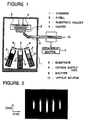
- FIG. 1 illustrates an apparatus for depositing a thin film on a substrate which is used in an example of the present invention.
- Fig. 2 is a RHEED pattern of a thin film of Bi2 Sr2 Can-1 Cun Ox which was grown to a thickness of 500 Å in the example according to the present invention.
- Now, the present invention will be described with reference to Examples, but the scope of the invention should not be limited to the Examples.
- At first, an intermediate layer of a compound oxide of La-Sr-Cu system was deposited on a {100} plane of a SrTiO3 single crystal substrate by RF (radio-frequency) sputtering under a film-forming condition shown in Table 1 (1). Then, a thin film of a superconducting compound oxide of Bi-Sr-Ca-Cu system was deposited by RF sputtering on the resulting intermediate layer under a film-forming condition shown in Table 1 (2).
Table 1 (1) Film-forming condition for the intermediate layer Composition of a target used La:Sr:Cu = 2.0 : 0.2 : 1.6 Sputtering gas Ar + O2 O2 / Ar + O2 0.2 (volume ratio) Sputtering gas pressure (Torr) 2 x 10⁻² Substrate temperature (°C) 800 RF-frequency power 50 W 0.64 W/cm2 Thickness of film (Å) 2,000 Table 1 (2) Film-forming condition for the superconductor layer Composition of a target used Bi:Sr:Ca:Cu = 2.6 : 2.0 : 2.0 : 3.0 Sputtering gas Ar + O2 O2 / Ar + O2 0.2 (ratio in volume) Sputtering gas pressure (Torr) 2 x 10⁻² Substrate temperature (°C) 750 RF-frequency power 50 W 0.64 W/cm2 Thickness of film (Å) 4,000 - As a comparative example, another superconductor layer was deposited directly on a SrTiO3 single crystal substrate under the same film-forming condition as is shown in Table 1 (2).
- The resulting samples of the present invention and of the comparative example were subjected to postannealing which was effected by the steps of heating the samples up to 890 °C at a rate of 3 °C/min in an oxygen stream, maintaining the samples at 890 °C for one hour, and then cooling down to room temperature at a rate of 3 °C/min.
- The samples had following compositions (atomic ratio):
Intermediate layer : La:Sr:Cu = 1.85 : 0.15 : 1 Thin film layer of superconductor : Bi:Sr:Ca:Cu = 2 : 2 : 2 : 3 - The samples were evaluated by measuring the critical temperature "Tc" and the critical current density "Jc". The results are shown in Table 2.
Table 2 Critical temperature (K) Invention comparative Tco(1) 115 115 Tci(2) 96 98 Critical current density (A/cm2)(3) 7.5 x 10⁵ 1.2 x 10⁴ (note)
(1) : a temperature where resistance started to drop.(2) : a temperature from which resistance could not be measured (3) : at 77 K - Table 2 reveals that higher critical current density is obtained in the sample according to the present invention without spoiling the other properties.
- The crystal structure of the samples were evaluated by an electron diffraction analyzer to find that the superconducting thin film in the sample of the present invention grow epitaxially.
- In this example, a vacuum deposition technique was used. A plurality of vapour sources were energized simultaneously. At first, an intermediate layer of compound oxide of Y-Ba-Cu system was deposited on a {100} plane of MgO single crystal substrate and then a superconducting compound oxide of Bi-Sr-Ca-Cu system was deposited on the resulting intermediate layer.
- As the vapour sources, commercially available metallic Y, Bi, Ca, Cu and fluorides of BaF2 and SrF2 were used. Metal elements were evaporated by means of K-cells while BaF2 and SrF2 were evaporated by electron guns. Table 3 (1) and (2) show film forming conditions.
Table 3 (1) Film-forming condition for the intermediate layer Partial pressure of oxygen (Torr) 2 x 10⁻⁵ Substrate temperature (°C) 700 Film-forming speed (Å/sec) 5 Thickness of film (Å) 2,000 Table 3 (2) Film-forming condition for the superconductor layer Partial pressure of oxygen (Torr) 2 x 10⁻⁵ Substrate temperature (°C) 750 Film-forming speed (Å/sec) 5 Thickness of film (Å) 4,000 - As a comparative example, another superconductor layer was deposited directly on a MgO single crystal substrate under the same film-forming condition as is shown in Table 3 (2).
- The resulting samples of the present invention and of the comparative example were subjected to post-annealing which was effected by the steps of heating the samples up to 890 °C at a rate of 3 °C/min in an oxygen stream, maintaining the samples at 890 °C for one hour, and then cooling down to room temperature at a rate of 3 °C/min.
- The samples had following compositions (atomic ratio):
Intermediate layer: Y:Ba:Cu = 1 : 2 : 3 Thin film layer of superconductor: Bi:Sr:Ca:Cu = 2 : 2 : 2 : 3 - The samples were evaluated by measuring the critical temperature "Tc" and the critical current density "Jc". The results are shown in Table 4.
Table 4 Critical temperature (K) Invention comparative Tco(1) 112 113 Tci(2) 90 95 Critical current density (A/cm2)(3) 5.4 x 10⁵ 7.7 x 10³ (note)
(1) : a temperature where resistance started to drop.(2) : a temperature from which resistance could not be measured (3) : at 77 K - Table 4 reveals that very higher critical current density is obtained in the sample according to the present invention.
- The crystal structure of the samples were evaluated by an electron diffraction analyzer to find that the superconducting thin film in the sample of the present invention grow epitaxially.
- At first, a thin film of an oxide of La-Cu was deposited on a {100} plane of a MgO single crystal substrate having a diameter of 15 mm by RF (radio-frequency) sputtering under a film-forming condition shown in Table 4 (1). Then, a thin film of an oxide of Y-Ba-Cu system was deposited by RF sputtering on the La-Cu oxide layer under a film-forming condition shown in Table 4 (2) to prepare a
sample 1. - A
comparative sample 2 was prepared by depositing the thin film of an oxide of Y-Ba-Cu directly on a MgO single crystal substrate under the same film-forming condition as is shown in Table 4 (2).Table 4 (1) Film-forming condition for a La-Cu oxide layer Composition of a target used La : Cu = 2.0 : 1.6 Sputtering gas Ar + O2 O2 / Ar + O2 0.2 (volume ratio) Sputtering gas pressure (Torr) : 4 x 10⁻² Substrate temperature (°C) 800 RF-frequency power 50 W 0.64 W/cm2 Thickness of film (Å) 2,000 Table 4 (2) Film-forming condition for a Y-Ba-Cu oxide layer Composition of a target used Y:Ba:Cu = 1.0 : 2.0 : 4.0 Sputtering gas Ar + O2 O2 / Ar + O2 0.2 (ratio in volume) Sputtering gas pressure (Torr) 2 x 10⁻² Substrate temperature (°C) 650 RF-frequency power 50 W 0.64 W/cm2 Thickness of film (Å) 4,000 - The resulting samples of the present invention and of the comparative example were subjected to post-annealing which was effected by the steps of heating the samples up to 900 °C at a rate of 3 °C/min in an oxygen stream, maintaining the samples at 900 °C for one hour, and then cooling down to room temperature at a rate of 3 °C/min.
- The samples were evaluated by measuring the critical temperature "Tco and Tci" and the critical current density "Jc". The results are shown in Table 5.
Table 5 Critical temperature (K) * Invention (Sample 1) comparative (Sample 2) Tco 90 88 Tci 87 88 Critical current density ** (A/cm2) 1.4 x 10⁶ 2.8 x 10⁴ (note)
(*) : "Tco" is a temperature where resistance started to drop. "Tci" is a temperature from which resistance could not be measured(**) : determined at 77 K - Table 5 reveals that higher critical current density is realized in the
sample 1 according to the present invention without spoiling the other properties. - The crystal structure of the samples were evaluated by an electron diffraction analysis to find that the superconducting thin film in the
sample 1 according to the present invention grow epitaxially while the superconducting thin film of thecomparative sample 2 did not grow epitaxially. - From the examples, it was confirmed that superconducting thin films of compound oxides having high critical current density can be produced in a reproducible manner.
Claims (4)
- A substrate having a superconducting thin film of compound oxide theron, an intermediate layer being interposed between said substrate and said superconducting thin film, characterised in that said intermediate layer consists of at least one layer of copper-containing compound oxide represented by the formula (I) or (II) :
(La1-xαx)2CuO4-y (I)
in which 〈〈 α 〉〉 stands for Sr or Ba, and 〈〈 x 〉〉 and 〈〈 y 〉〉 are numbers each satisfying respective range of 0 ≤ x <1 and 0 ≤ y < 1,
Ln1Ba2Cu307-z (II)
in which 〈〈 Ln 〉〉 stands for at least one element selected from a group comprising La, Ce, Pr, Nd, Sm, Eu, Gd, Tb, Dy, Ho, Y, Er, Tm, Yb, and Lu, and 〈〈 z 〉〉 is a number satisfying a range of 0 ≤ z < 1, and said superconducting thin film is formed of a compound oxide of formula :
Bi4(Sr1-xCax)mCunOp+y (III)
in which 〈〈 x 〉〉 〈〈 m 〉〉, 〈〈 n 〉〉, 〈〈 p 〉〉 and 〈〈 y 〉〉 are numbers each satisfying ranges of 6 ≤ m ≤ 10, 4 ≤ n ≤ 8, 0 < x <1, and -2 ≤ y ≤ +2 respectively and
Ln'1Ba2Cu3O7-z (IV)
in which 〈〈 Ln' 〉〉 stands for at least one element selected from a group comprising La, Nd, Sm, Eu, Gd, Dy, Ho, Y, Er, Tm, Yb and Lu, and 〈〈 z 〉〉 is a number satisfying a range of 0 ≤ z < 1, with the proviso that the copper-containing compound oxide of the intermediate layer is represented by formula (I) when the compound oxide of the superconducting thin film is represented by formula (IV). - The substrate set forth in claim 1 wherein said substrate is a single crystal of an oxide.
- The substrate set forth in claim 2 wherein said substrate is a single crystal of an oxide selected from a group comprising MgO, SrTiO3 and YSZ.
- The substrate set forth in claim 1 wherein said intermediate layer has a crystal structure of perovskite or layered preovskite.
Priority Applications (1)
| Application Number | Priority Date | Filing Date | Title |
|---|---|---|---|
| EP19940201833 EP0619283A3 (en) | 1989-06-30 | 1990-07-02 | Substrate having a superconductor layer. |
Applications Claiming Priority (6)
| Application Number | Priority Date | Filing Date | Title |
|---|---|---|---|
| JP168677/89 | 1989-06-30 | ||
| JP16867789 | 1989-06-30 | ||
| JP19101489 | 1989-07-24 | ||
| JP191014/89 | 1989-07-24 | ||
| JP33891689 | 1989-12-27 | ||
| JP338916/89 | 1989-12-27 |
Related Child Applications (1)
| Application Number | Title | Priority Date | Filing Date |
|---|---|---|---|
| EP94201833.4 Division-Into | 1994-06-27 |
Publications (3)
| Publication Number | Publication Date |
|---|---|
| EP0406126A1 EP0406126A1 (en) | 1991-01-02 |
| EP0406126B1 EP0406126B1 (en) | 1995-01-25 |
| EP0406126B2 true EP0406126B2 (en) | 1997-12-17 |
Family
ID=27323043
Family Applications (2)
| Application Number | Title | Priority Date | Filing Date |
|---|---|---|---|
| EP19940201833 Withdrawn EP0619283A3 (en) | 1989-06-30 | 1990-07-02 | Substrate having a superconductor layer. |
| EP90401911A Expired - Lifetime EP0406126B2 (en) | 1989-06-30 | 1990-07-02 | Substrate having a superconductor layer |
Family Applications Before (1)
| Application Number | Title | Priority Date | Filing Date |
|---|---|---|---|
| EP19940201833 Withdrawn EP0619283A3 (en) | 1989-06-30 | 1990-07-02 | Substrate having a superconductor layer. |
Country Status (5)
| Country | Link |
|---|---|
| US (1) | US5712227A (en) |
| EP (2) | EP0619283A3 (en) |
| AU (1) | AU635040B2 (en) |
| CA (1) | CA2020302C (en) |
| DE (1) | DE69016283T3 (en) |
Families Citing this family (15)
| Publication number | Priority date | Publication date | Assignee | Title |
|---|---|---|---|---|
| AU635136B2 (en) * | 1990-05-30 | 1993-03-11 | Sumitomo Electric Industries, Ltd. | Process for preparing high-temperature superconducting thin films |
| DE69127719T2 (en) * | 1990-05-30 | 1998-03-05 | Sumitomo Electric Industries | Process for the production of a superconducting transition from oxidic superconductor |
| CA2045890C (en) * | 1990-06-28 | 1998-10-06 | Takashi Matsuura | Process for preparing thin film of oxide superconductor |
| US5508255A (en) * | 1994-07-05 | 1996-04-16 | Superconductor Technologies, Inc. | Epitaxial thallium high temperature superconducting films formed via a nucleation layer |
| GB9424766D0 (en) * | 1994-12-07 | 1995-02-08 | Wellcome Found | Pharmaceutical composition |
| DE19544698C1 (en) * | 1995-11-30 | 1997-06-05 | Abb Research Ltd | Magnesium oxide substrate containing copper oxide |
| US6602588B1 (en) * | 1998-09-14 | 2003-08-05 | The Regents Of The University Of California | Superconducting structure including mixed rare earth barium-copper compositions |
| US6541136B1 (en) * | 1998-09-14 | 2003-04-01 | The Regents Of The University Of California | Superconducting structure |
| WO2003034448A1 (en) * | 2000-12-06 | 2003-04-24 | The Regents Of The University Of California | Superconducting composite structures |
| US6709989B2 (en) | 2001-06-21 | 2004-03-23 | Motorola, Inc. | Method for fabricating a semiconductor structure including a metal oxide interface with silicon |
| US20020195057A1 (en) * | 2001-06-21 | 2002-12-26 | Motorola, Inc. | Apparatus for fabricating semiconductor structures and method of forming the same |
| US6693298B2 (en) | 2001-07-20 | 2004-02-17 | Motorola, Inc. | Structure and method for fabricating epitaxial semiconductor on insulator (SOI) structures and devices utilizing the formation of a compliant substrate for materials used to form same |
| US6716545B1 (en) * | 2001-11-21 | 2004-04-06 | The Regents Of The University Of California | High temperature superconducting composite conductors |
| DE10248962B4 (en) * | 2002-10-21 | 2007-10-25 | THEVA DüNNSCHICHTTECHNIK GMBH | Process for producing a high temperature superconductor layer |
| US6806202B2 (en) | 2002-12-03 | 2004-10-19 | Motorola, Inc. | Method of removing silicon oxide from a surface of a substrate |
Family Cites Families (21)
| Publication number | Priority date | Publication date | Assignee | Title |
|---|---|---|---|---|
| KR910002311B1 (en) * | 1987-02-27 | 1991-04-11 | 가부시기가이샤 히다찌세이사꾸쇼 | A superconductor device |
| EP0283312A3 (en) * | 1987-03-20 | 1990-09-26 | Fujikura Ltd. | Method of producing a superconducting wire and a superconducting wire produced according to the same |
| US4983575A (en) * | 1987-03-25 | 1991-01-08 | Hitachi, Ltd. | Superconducting thin films made of stacked composite oxide layers |
| US5057484A (en) * | 1987-05-01 | 1991-10-15 | Fujikura Ltd. | Single crystal oxide superconductor and method of producing the same |
| JPS63283085A (en) * | 1987-05-15 | 1988-11-18 | Hitachi Ltd | Superconducting device |
| JPH0776155B2 (en) * | 1987-06-26 | 1995-08-16 | 古河電気工業株式会社 | Method for manufacturing ceramic superconducting compact |
| NL8701779A (en) * | 1987-07-28 | 1989-02-16 | Philips Nv | SUPER CONDUCTIVE THIN LAYER. |
| JPS6431475A (en) * | 1987-07-28 | 1989-02-01 | Univ Tokyo | Superconducting device and forming method thereof |
| US4980339A (en) * | 1987-07-29 | 1990-12-25 | Matsushita Electric Industrial Co., Ltd. | Superconductor structure |
| NL8701788A (en) * | 1987-07-29 | 1989-02-16 | Philips Nv | METHOD FOR MANUFACTURING A SUPER-CONDUCTIVE THIN LAYER |
| US5079222A (en) * | 1987-08-31 | 1992-01-07 | Semiconductor Energy Laboratory Co., Ltd. | Superconducting ceramic circuits and manufacturing method for the same |
| KR910007384B1 (en) * | 1987-09-16 | 1991-09-25 | 가부시끼가이샤 한도다이 에네르기 겐뀨쇼 | Formation of superconductor oxide film |
| EP0325877B1 (en) * | 1987-12-26 | 1994-03-09 | Sumitomo Electric Industries Limited | A semiconductor substrate having a superconducting thin film |
| US5084438A (en) * | 1988-03-23 | 1992-01-28 | Nec Corporation | Electronic device substrate using silicon semiconductor substrate |
| US5034359A (en) * | 1988-04-08 | 1991-07-23 | Kabushiki Kaisha Toshiba | Insulating composition |
| KR900017216A (en) * | 1988-04-30 | 1990-11-15 | 나까하라 쯔네오 | Semiconductor Substrate Having Superconductor Thin Film and Its Manufacturing Method |
| US5232900A (en) * | 1988-06-09 | 1993-08-03 | Superconductor Development Corporation | Superconductor structure |
| US5034378A (en) * | 1988-12-15 | 1991-07-23 | James P. Cox | Synergistic flavor enhancement nutritional compositions and methods |
| US5087605A (en) * | 1989-06-01 | 1992-02-11 | Bell Communications Research, Inc. | Layered lattice-matched superconducting device and method of making |
| US5118663A (en) * | 1990-09-21 | 1992-06-02 | General Atomics | Fabrication of silver coated high temperature ceramic superconductor fiber with metal substrate |
| US5162294A (en) * | 1991-02-28 | 1992-11-10 | Westinghouse Electric Corp. | Buffer layer for copper oxide based superconductor growth on sapphire |
-
1990
- 1990-07-02 EP EP19940201833 patent/EP0619283A3/en not_active Withdrawn
- 1990-07-02 EP EP90401911A patent/EP0406126B2/en not_active Expired - Lifetime
- 1990-07-02 DE DE69016283T patent/DE69016283T3/en not_active Expired - Fee Related
- 1990-07-02 AU AU58606/90A patent/AU635040B2/en not_active Ceased
- 1990-07-03 CA CA002020302A patent/CA2020302C/en not_active Expired - Fee Related
-
1995
- 1995-01-25 US US08/378,895 patent/US5712227A/en not_active Expired - Fee Related
Also Published As
| Publication number | Publication date |
|---|---|
| US5712227A (en) | 1998-01-27 |
| CA2020302C (en) | 1995-06-27 |
| DE69016283T2 (en) | 1995-08-03 |
| AU635040B2 (en) | 1993-03-11 |
| EP0619283A2 (en) | 1994-10-12 |
| AU5860690A (en) | 1991-01-10 |
| DE69016283T3 (en) | 1998-04-02 |
| EP0406126A1 (en) | 1991-01-02 |
| EP0619283A3 (en) | 1994-11-30 |
| CA2020302A1 (en) | 1991-01-25 |
| DE69016283D1 (en) | 1995-03-09 |
| EP0406126B1 (en) | 1995-01-25 |
Similar Documents
| Publication | Publication Date | Title |
|---|---|---|
| EP0406126B2 (en) | Substrate having a superconductor layer | |
| US5372992A (en) | Superconducting thin film | |
| US4988670A (en) | Method of forming oxide superconducting films by in-situ annealing | |
| EP0446145B1 (en) | Process for preparing high-temperature superconducting thin films | |
| US5179070A (en) | Semiconductor substrate having a superconducting thin film with a buffer layer in between | |
| US5428005A (en) | Superconducting thin film of compound oxide and a process of preparing the same | |
| US5135906A (en) | Superconducting thin film of compound oxide and process for preparing the same | |
| EP0347335B1 (en) | A superconducting thin film and a process for depositing the same | |
| EP0322306B1 (en) | Process for producing a superconducting thin film | |
| EP0341148B1 (en) | A semiconductor substrate having a superconducting thin film | |
| US5051398A (en) | Process for preparing a bismuth-type superconducting thin film | |
| US5252543A (en) | Superconducting thin film and wire on a smooth substrate | |
| US5240904A (en) | Process for preparing a-axis oriented superconducting oxide thin films | |
| EP0459906B1 (en) | Process for preparing superconducting junction of oxide superconductor | |
| US5296455A (en) | Process for preparing superconductor of compound oxide of Bi-Sr-Ca-Cu system | |
| US5236894A (en) | Process for producing a superconducting thin film at relatively low temperature | |
| US5260267A (en) | Method for forming a Bi-containing superconducting oxide film on a substrate with a buffer layer of Bi2 O3 | |
| US5252553A (en) | Process for preparing a superconducting thin film of compound oxide | |
| US5314870A (en) | Preparing thin film of oxide superconductor |
Legal Events
| Date | Code | Title | Description |
|---|---|---|---|
| PUAI | Public reference made under article 153(3) epc to a published international application that has entered the european phase |
Free format text: ORIGINAL CODE: 0009012 |
|
| AK | Designated contracting states |
Kind code of ref document: A1 Designated state(s): DE FR GB IT NL |
|
| 17P | Request for examination filed |
Effective date: 19901214 |
|
| 17Q | First examination report despatched |
Effective date: 19930810 |
|
| GRAA | (expected) grant |
Free format text: ORIGINAL CODE: 0009210 |
|
| AK | Designated contracting states |
Kind code of ref document: B1 Designated state(s): DE FR GB IT NL |
|
| REF | Corresponds to: |
Ref document number: 69016283 Country of ref document: DE Date of ref document: 19950309 |
|
| ITF | It: translation for a ep patent filed | ||
| ET | Fr: translation filed | ||
| PLBI | Opposition filed |
Free format text: ORIGINAL CODE: 0009260 |
|
| 26 | Opposition filed |
Opponent name: SIEMENS AG Effective date: 19951013 |
|
| PLBF | Reply of patent proprietor to notice(s) of opposition |
Free format text: ORIGINAL CODE: EPIDOS OBSO |
|
| NLR1 | Nl: opposition has been filed with the epo |
Opponent name: SIEMENS AG |
|
| PLBF | Reply of patent proprietor to notice(s) of opposition |
Free format text: ORIGINAL CODE: EPIDOS OBSO |
|
| PLAW | Interlocutory decision in opposition |
Free format text: ORIGINAL CODE: EPIDOS IDOP |
|
| PLAW | Interlocutory decision in opposition |
Free format text: ORIGINAL CODE: EPIDOS IDOP |
|
| PUAH | Patent maintained in amended form |
Free format text: ORIGINAL CODE: 0009272 |
|
| STAA | Information on the status of an ep patent application or granted ep patent |
Free format text: STATUS: PATENT MAINTAINED AS AMENDED |
|
| 27A | Patent maintained in amended form |
Effective date: 19971217 |
|
| AK | Designated contracting states |
Kind code of ref document: B2 Designated state(s): DE FR GB IT NL |
|
| ITF | It: translation for a ep patent filed | ||
| NLR2 | Nl: decision of opposition | ||
| ET3 | Fr: translation filed ** decision concerning opposition | ||
| NLR3 | Nl: receipt of modified translations in the netherlands language after an opposition procedure | ||
| REG | Reference to a national code |
Ref country code: GB Ref legal event code: IF02 |
|
| PGFP | Annual fee paid to national office [announced via postgrant information from national office to epo] |
Ref country code: GB Payment date: 20020626 Year of fee payment: 13 |
|
| PGFP | Annual fee paid to national office [announced via postgrant information from national office to epo] |
Ref country code: FR Payment date: 20020709 Year of fee payment: 13 |
|
| PGFP | Annual fee paid to national office [announced via postgrant information from national office to epo] |
Ref country code: DE Payment date: 20020710 Year of fee payment: 13 |
|
| PGFP | Annual fee paid to national office [announced via postgrant information from national office to epo] |
Ref country code: NL Payment date: 20020730 Year of fee payment: 13 |
|
| PG25 | Lapsed in a contracting state [announced via postgrant information from national office to epo] |
Ref country code: GB Free format text: LAPSE BECAUSE OF NON-PAYMENT OF DUE FEES Effective date: 20030702 |
|
| PG25 | Lapsed in a contracting state [announced via postgrant information from national office to epo] |
Ref country code: NL Free format text: LAPSE BECAUSE OF NON-PAYMENT OF DUE FEES Effective date: 20040201 |
|
| PG25 | Lapsed in a contracting state [announced via postgrant information from national office to epo] |
Ref country code: DE Free format text: LAPSE BECAUSE OF NON-PAYMENT OF DUE FEES Effective date: 20040203 |
|
| GBPC | Gb: european patent ceased through non-payment of renewal fee |
Effective date: 20030702 |
|
| PG25 | Lapsed in a contracting state [announced via postgrant information from national office to epo] |
Ref country code: FR Free format text: LAPSE BECAUSE OF NON-PAYMENT OF DUE FEES Effective date: 20040331 |
|
| NLV4 | Nl: lapsed or anulled due to non-payment of the annual fee |
Effective date: 20040201 |
|
| REG | Reference to a national code |
Ref country code: FR Ref legal event code: ST |
|
| PG25 | Lapsed in a contracting state [announced via postgrant information from national office to epo] |
Ref country code: IT Free format text: LAPSE BECAUSE OF NON-PAYMENT OF DUE FEES;WARNING: LAPSES OF ITALIAN PATENTS WITH EFFECTIVE DATE BEFORE 2007 MAY HAVE OCCURRED AT ANY TIME BEFORE 2007. THE CORRECT EFFECTIVE DATE MAY BE DIFFERENT FROM THE ONE RECORDED. Effective date: 20050702 |
|
| PLAB | Opposition data, opponent's data or that of the opponent's representative modified |
Free format text: ORIGINAL CODE: 0009299OPPO |