EP0710430B1 - Processing low dielectric constant materials for high speed electronics - Google Patents
Processing low dielectric constant materials for high speed electronics Download PDFInfo
- Publication number
- EP0710430B1 EP0710430B1 EP95920427A EP95920427A EP0710430B1 EP 0710430 B1 EP0710430 B1 EP 0710430B1 EP 95920427 A EP95920427 A EP 95920427A EP 95920427 A EP95920427 A EP 95920427A EP 0710430 B1 EP0710430 B1 EP 0710430B1
- Authority
- EP
- European Patent Office
- Prior art keywords
- layer
- dielectric constant
- porous
- low dielectric
- additive material
- Prior art date
- Legal status (The legal status is an assumption and is not a legal conclusion. Google has not performed a legal analysis and makes no representation as to the accuracy of the status listed.)
- Expired - Lifetime
Links
Images





Classifications
-
- H—ELECTRICITY
- H05—ELECTRIC TECHNIQUES NOT OTHERWISE PROVIDED FOR
- H05K—PRINTED CIRCUITS; CASINGS OR CONSTRUCTIONAL DETAILS OF ELECTRIC APPARATUS; MANUFACTURE OF ASSEMBLAGES OF ELECTRICAL COMPONENTS
- H05K1/00—Printed circuits
- H05K1/02—Details
- H05K1/03—Use of materials for the substrate
- H05K1/0313—Organic insulating material
-
- H—ELECTRICITY
- H05—ELECTRIC TECHNIQUES NOT OTHERWISE PROVIDED FOR
- H05K—PRINTED CIRCUITS; CASINGS OR CONSTRUCTIONAL DETAILS OF ELECTRIC APPARATUS; MANUFACTURE OF ASSEMBLAGES OF ELECTRICAL COMPONENTS
- H05K1/00—Printed circuits
- H05K1/02—Details
- H05K1/0213—Electrical arrangements not otherwise provided for
- H05K1/0237—High frequency adaptations
- H05K1/024—Dielectric details, e.g. changing the dielectric material around a transmission line
-
- H—ELECTRICITY
- H05—ELECTRIC TECHNIQUES NOT OTHERWISE PROVIDED FOR
- H05K—PRINTED CIRCUITS; CASINGS OR CONSTRUCTIONAL DETAILS OF ELECTRIC APPARATUS; MANUFACTURE OF ASSEMBLAGES OF ELECTRICAL COMPONENTS
- H05K1/00—Printed circuits
- H05K1/02—Details
- H05K1/03—Use of materials for the substrate
- H05K1/0313—Organic insulating material
- H05K1/0353—Organic insulating material consisting of two or more materials, e.g. two or more polymers, polymer + filler, + reinforcement
- H05K1/0373—Organic insulating material consisting of two or more materials, e.g. two or more polymers, polymer + filler, + reinforcement containing additives, e.g. fillers
-
- H—ELECTRICITY
- H05—ELECTRIC TECHNIQUES NOT OTHERWISE PROVIDED FOR
- H05K—PRINTED CIRCUITS; CASINGS OR CONSTRUCTIONAL DETAILS OF ELECTRIC APPARATUS; MANUFACTURE OF ASSEMBLAGES OF ELECTRICAL COMPONENTS
- H05K3/00—Apparatus or processes for manufacturing printed circuits
- H05K3/0011—Working of insulating substrates or insulating layers
- H05K3/0017—Etching of the substrate by chemical or physical means
- H05K3/0026—Etching of the substrate by chemical or physical means by laser ablation
- H05K3/0032—Etching of the substrate by chemical or physical means by laser ablation of organic insulating material
-
- H—ELECTRICITY
- H10—SEMICONDUCTOR DEVICES; ELECTRIC SOLID-STATE DEVICES NOT OTHERWISE PROVIDED FOR
- H10W—GENERIC PACKAGES, INTERCONNECTIONS, CONNECTORS OR OTHER CONSTRUCTIONAL DETAILS OF DEVICES COVERED BY CLASS H10
- H10W70/00—Package substrates; Interposers; Redistribution layers [RDL]
- H10W70/01—Manufacture or treatment
- H10W70/05—Manufacture or treatment of insulating or insulated package substrates, or of interposers, or of redistribution layers
- H10W70/093—Connecting or disconnecting other interconnections thereto or therefrom, e.g. connecting bond wires or bumps
-
- H—ELECTRICITY
- H10—SEMICONDUCTOR DEVICES; ELECTRIC SOLID-STATE DEVICES NOT OTHERWISE PROVIDED FOR
- H10W—GENERIC PACKAGES, INTERCONNECTIONS, CONNECTORS OR OTHER CONSTRUCTIONAL DETAILS OF DEVICES COVERED BY CLASS H10
- H10W70/00—Package substrates; Interposers; Redistribution layers [RDL]
- H10W70/60—Insulating or insulated package substrates; Interposers; Redistribution layers
- H10W70/611—Insulating or insulated package substrates; Interposers; Redistribution layers for connecting multiple chips together
- H10W70/614—Insulating or insulated package substrates; Interposers; Redistribution layers for connecting multiple chips together the multiple chips being integrally enclosed
-
- H—ELECTRICITY
- H10—SEMICONDUCTOR DEVICES; ELECTRIC SOLID-STATE DEVICES NOT OTHERWISE PROVIDED FOR
- H10W—GENERIC PACKAGES, INTERCONNECTIONS, CONNECTORS OR OTHER CONSTRUCTIONAL DETAILS OF DEVICES COVERED BY CLASS H10
- H10W70/00—Package substrates; Interposers; Redistribution layers [RDL]
- H10W70/60—Insulating or insulated package substrates; Interposers; Redistribution layers
- H10W70/67—Insulating or insulated package substrates; Interposers; Redistribution layers characterised by their insulating layers or insulating parts
- H10W70/69—Insulating materials thereof
-
- H—ELECTRICITY
- H10—SEMICONDUCTOR DEVICES; ELECTRIC SOLID-STATE DEVICES NOT OTHERWISE PROVIDED FOR
- H10W—GENERIC PACKAGES, INTERCONNECTIONS, CONNECTORS OR OTHER CONSTRUCTIONAL DETAILS OF DEVICES COVERED BY CLASS H10
- H10W99/00—Subject matter not provided for in other groups of this subclass
-
- H—ELECTRICITY
- H05—ELECTRIC TECHNIQUES NOT OTHERWISE PROVIDED FOR
- H05K—PRINTED CIRCUITS; CASINGS OR CONSTRUCTIONAL DETAILS OF ELECTRIC APPARATUS; MANUFACTURE OF ASSEMBLAGES OF ELECTRICAL COMPONENTS
- H05K2201/00—Indexing scheme relating to printed circuits covered by H05K1/00
- H05K2201/01—Dielectrics
- H05K2201/0104—Properties and characteristics in general
- H05K2201/0116—Porous, e.g. foam
-
- H—ELECTRICITY
- H05—ELECTRIC TECHNIQUES NOT OTHERWISE PROVIDED FOR
- H05K—PRINTED CIRCUITS; CASINGS OR CONSTRUCTIONAL DETAILS OF ELECTRIC APPARATUS; MANUFACTURE OF ASSEMBLAGES OF ELECTRICAL COMPONENTS
- H05K2201/00—Indexing scheme relating to printed circuits covered by H05K1/00
- H05K2201/01—Dielectrics
- H05K2201/0137—Materials
- H05K2201/015—Fluoropolymer, e.g. polytetrafluoroethylene [PTFE]
-
- H—ELECTRICITY
- H05—ELECTRIC TECHNIQUES NOT OTHERWISE PROVIDED FOR
- H05K—PRINTED CIRCUITS; CASINGS OR CONSTRUCTIONAL DETAILS OF ELECTRIC APPARATUS; MANUFACTURE OF ASSEMBLAGES OF ELECTRICAL COMPONENTS
- H05K2201/00—Indexing scheme relating to printed circuits covered by H05K1/00
- H05K2201/01—Dielectrics
- H05K2201/0137—Materials
- H05K2201/0158—Polyalkene or polyolefin, e.g. polyethylene [PE], polypropylene [PP]
-
- H—ELECTRICITY
- H05—ELECTRIC TECHNIQUES NOT OTHERWISE PROVIDED FOR
- H05K—PRINTED CIRCUITS; CASINGS OR CONSTRUCTIONAL DETAILS OF ELECTRIC APPARATUS; MANUFACTURE OF ASSEMBLAGES OF ELECTRICAL COMPONENTS
- H05K2203/00—Indexing scheme relating to apparatus or processes for manufacturing printed circuits covered by H05K3/00
- H05K2203/08—Treatments involving gases
- H05K2203/083—Evaporation or sublimation of a compound, e.g. gas bubble generating agent
-
- H—ELECTRICITY
- H05—ELECTRIC TECHNIQUES NOT OTHERWISE PROVIDED FOR
- H05K—PRINTED CIRCUITS; CASINGS OR CONSTRUCTIONAL DETAILS OF ELECTRIC APPARATUS; MANUFACTURE OF ASSEMBLAGES OF ELECTRICAL COMPONENTS
- H05K2203/00—Indexing scheme relating to apparatus or processes for manufacturing printed circuits covered by H05K3/00
- H05K2203/12—Using specific substances
- H05K2203/122—Organic non-polymeric compounds, e.g. oil, wax or thiol
-
- H—ELECTRICITY
- H05—ELECTRIC TECHNIQUES NOT OTHERWISE PROVIDED FOR
- H05K—PRINTED CIRCUITS; CASINGS OR CONSTRUCTIONAL DETAILS OF ELECTRIC APPARATUS; MANUFACTURE OF ASSEMBLAGES OF ELECTRICAL COMPONENTS
- H05K3/00—Apparatus or processes for manufacturing printed circuits
- H05K3/38—Improvement of the adhesion between the insulating substrate and the metal
- H05K3/386—Improvement of the adhesion between the insulating substrate and the metal by the use of an organic polymeric bonding layer, e.g. adhesive
-
- H—ELECTRICITY
- H10—SEMICONDUCTOR DEVICES; ELECTRIC SOLID-STATE DEVICES NOT OTHERWISE PROVIDED FOR
- H10W—GENERIC PACKAGES, INTERCONNECTIONS, CONNECTORS OR OTHER CONSTRUCTIONAL DETAILS OF DEVICES COVERED BY CLASS H10
- H10W70/00—Package substrates; Interposers; Redistribution layers [RDL]
- H10W70/099—Connecting interconnections to insulating or insulated package substrates, interposers or redistribution layers
-
- H—ELECTRICITY
- H10—SEMICONDUCTOR DEVICES; ELECTRIC SOLID-STATE DEVICES NOT OTHERWISE PROVIDED FOR
- H10W—GENERIC PACKAGES, INTERCONNECTIONS, CONNECTORS OR OTHER CONSTRUCTIONAL DETAILS OF DEVICES COVERED BY CLASS H10
- H10W70/00—Package substrates; Interposers; Redistribution layers [RDL]
- H10W70/60—Insulating or insulated package substrates; Interposers; Redistribution layers
-
- H—ELECTRICITY
- H10—SEMICONDUCTOR DEVICES; ELECTRIC SOLID-STATE DEVICES NOT OTHERWISE PROVIDED FOR
- H10W—GENERIC PACKAGES, INTERCONNECTIONS, CONNECTORS OR OTHER CONSTRUCTIONAL DETAILS OF DEVICES COVERED BY CLASS H10
- H10W70/00—Package substrates; Interposers; Redistribution layers [RDL]
- H10W70/60—Insulating or insulated package substrates; Interposers; Redistribution layers
- H10W70/67—Insulating or insulated package substrates; Interposers; Redistribution layers characterised by their insulating layers or insulating parts
- H10W70/68—Shapes or dispositions thereof
- H10W70/682—Shapes or dispositions thereof comprising holes having chips therein
-
- H—ELECTRICITY
- H10—SEMICONDUCTOR DEVICES; ELECTRIC SOLID-STATE DEVICES NOT OTHERWISE PROVIDED FOR
- H10W—GENERIC PACKAGES, INTERCONNECTIONS, CONNECTORS OR OTHER CONSTRUCTIONAL DETAILS OF DEVICES COVERED BY CLASS H10
- H10W72/00—Interconnections or connectors in packages
- H10W72/071—Connecting or disconnecting
- H10W72/073—Connecting or disconnecting of die-attach connectors
-
- H—ELECTRICITY
- H10—SEMICONDUCTOR DEVICES; ELECTRIC SOLID-STATE DEVICES NOT OTHERWISE PROVIDED FOR
- H10W—GENERIC PACKAGES, INTERCONNECTIONS, CONNECTORS OR OTHER CONSTRUCTIONAL DETAILS OF DEVICES COVERED BY CLASS H10
- H10W72/00—Interconnections or connectors in packages
- H10W72/851—Dispositions of multiple connectors or interconnections
- H10W72/874—On different surfaces
-
- H—ELECTRICITY
- H10—SEMICONDUCTOR DEVICES; ELECTRIC SOLID-STATE DEVICES NOT OTHERWISE PROVIDED FOR
- H10W—GENERIC PACKAGES, INTERCONNECTIONS, CONNECTORS OR OTHER CONSTRUCTIONAL DETAILS OF DEVICES COVERED BY CLASS H10
- H10W90/00—Package configurations
-
- H—ELECTRICITY
- H10—SEMICONDUCTOR DEVICES; ELECTRIC SOLID-STATE DEVICES NOT OTHERWISE PROVIDED FOR
- H10W—GENERIC PACKAGES, INTERCONNECTIONS, CONNECTORS OR OTHER CONSTRUCTIONAL DETAILS OF DEVICES COVERED BY CLASS H10
- H10W90/00—Package configurations
- H10W90/701—Package configurations characterised by the relative positions of pads or connectors relative to package parts
- H10W90/731—Package configurations characterised by the relative positions of pads or connectors relative to package parts of die-attach connectors
- H10W90/734—Package configurations characterised by the relative positions of pads or connectors relative to package parts of die-attach connectors between a chip and a stacked insulating package substrate, interposer or RDL
-
- Y—GENERAL TAGGING OF NEW TECHNOLOGICAL DEVELOPMENTS; GENERAL TAGGING OF CROSS-SECTIONAL TECHNOLOGIES SPANNING OVER SEVERAL SECTIONS OF THE IPC; TECHNICAL SUBJECTS COVERED BY FORMER USPC CROSS-REFERENCE ART COLLECTIONS [XRACs] AND DIGESTS
- Y10—TECHNICAL SUBJECTS COVERED BY FORMER USPC
- Y10S—TECHNICAL SUBJECTS COVERED BY FORMER USPC CROSS-REFERENCE ART COLLECTIONS [XRACs] AND DIGESTS
- Y10S521/00—Synthetic resins or natural rubbers -- part of the class 520 series
- Y10S521/918—Physical aftertreatment of a cellular product
-
- Y—GENERAL TAGGING OF NEW TECHNOLOGICAL DEVELOPMENTS; GENERAL TAGGING OF CROSS-SECTIONAL TECHNOLOGIES SPANNING OVER SEVERAL SECTIONS OF THE IPC; TECHNICAL SUBJECTS COVERED BY FORMER USPC CROSS-REFERENCE ART COLLECTIONS [XRACs] AND DIGESTS
- Y10—TECHNICAL SUBJECTS COVERED BY FORMER USPC
- Y10T—TECHNICAL SUBJECTS COVERED BY FORMER US CLASSIFICATION
- Y10T29/00—Metal working
- Y10T29/49—Method of mechanical manufacture
- Y10T29/49002—Electrical device making
- Y10T29/49117—Conductor or circuit manufacturing
- Y10T29/49124—On flat or curved insulated base, e.g., printed circuit, etc.
-
- Y—GENERAL TAGGING OF NEW TECHNOLOGICAL DEVELOPMENTS; GENERAL TAGGING OF CROSS-SECTIONAL TECHNOLOGIES SPANNING OVER SEVERAL SECTIONS OF THE IPC; TECHNICAL SUBJECTS COVERED BY FORMER USPC CROSS-REFERENCE ART COLLECTIONS [XRACs] AND DIGESTS
- Y10—TECHNICAL SUBJECTS COVERED BY FORMER USPC
- Y10T—TECHNICAL SUBJECTS COVERED BY FORMER US CLASSIFICATION
- Y10T29/00—Metal working
- Y10T29/49—Method of mechanical manufacture
- Y10T29/49002—Electrical device making
- Y10T29/49117—Conductor or circuit manufacturing
- Y10T29/49124—On flat or curved insulated base, e.g., printed circuit, etc.
- Y10T29/49155—Manufacturing circuit on or in base
Definitions
- This invention relates generally to low dielectric constant porous materials and, more particularly, to a process for using porous layers in printed circuit boards and over electronic circuits and supporting substrates.
- Porous polytetrafluoroethylene (PTFE) materials such as GortexTM (Gortex is a trademark of W.L. Gore & Associates, Inc., of Newark, DE) have excellent low dielectric constant properties, but unfortunately they absorb process chemicals in their pores during MCM (multichip module) or PC (printed circuit) board processing that cannot be removed. Additionally, the fact that the porous material deforms during pressurized processing destroys its porous properties, and therefore the deformed material does not provide the desired consistent low dielectric constant.
- the DuPont Teflon polytetrafluoroethylene line of materials has intrinsically low dielectric constants and has the necessary high temperature stability for most industrial and military uses.
- Gortex material is a Teflon PTFE-based material that is filled with micro-pores that create a foam-like cloth material.
- Porous PTFE material is generally used in clothes to simultaneously provide warmth and allow perspiration and moisture vapors to vent through its pores.
- Porous PTFE material is alternatively sold as a filled porous PTFE material.
- a filled porous material is disclosed in U.S. Patent No. 5,034,801. Unfilled porous PTFE material is an excellent candidate for high frequency circuits because the dielectric constant can be significantly less than that found in other materials. However, in laminant applications and processing, the pores can collapse under pressure and/or be filled witn processing materials during fabrication which cannot be easily removed.
- Ceramic foam materials are discussed, for example, in “Giants in advanced ceramics,” Ceramic Industry, vol. 141, 47 (March 1993), and Te-Kao Wu, "Dielectric properties measurement of substrate and support materials,” Microwave and Optical Technology Letters, vol. 3, 283-286 (March 1990). These materials, however, are inflexible and not fabricated in large area sections. Because the ceramic foam materials are inflexible, they can be used as substrates but cannot be used in overlay technologies that are not perfectly flat. Because ceramic foam materials are fragile, they are typically not capable of withstanding PC board lamination processing in their intrinsic state. Furthermore, ceramic foam materials can be filled with processing materials which degrade their low dielectric constant.
- porous PTFE material and ceramic foam material
- the metal tends to extend into the pores and it is thus difficult to achieve a smooth and continuous metal surface for use in high frequency applications where skin-effect related losses are of importance.
- Polymer materials in high frequency circuits are preferably laser ablatable by ultraviolet light in order to form the via openings through which different layers of metallization are connected.
- Laser processing is normally done with several passes of the laser beam with a power ranging from 0.5 to 2.0 watts, with a preferred maximum power level being about 1.5 watts.
- a dielectric layer is characterized as being laser ablatable, it means that such layer can be totally removed by progressive passes of a laser beam of this power level, and when it is characterized as not being laser ablatable, it means that a layer is not completely removed by progressive passes of such a laser beam.
- One method of adaptive laser ablation is discussed in Eichelberger et al., U.S.
- Most polytetrafluoroethylene materials are not laser ablatable and generally do not easily adhere to other materials.
- a method of modifying the ultraviolet absorption characteristics of a polymer material with the addition of an ultraviolet absorbing dye is discussed is Cole et al., U.S. Patent No. 5,169,678.
- preferred materials are those which can be processed at a laser frequency of 351 nm.
- This frequency was selected in accordance with the characteristics of desirable dielectric layers such as KaptonTM polyimide (Kapton is a trademark of E.I. DuPont de Nemours and Co.) and the fact that there are commercial photoresists which can be processed at this frequency.
- UltemTM polyetherimide resin Ultem is a registered trademark of General Electric Co.
- the Ultem polyetherimide resin is laser ablatable at 351 nm.
- PC boards typically have dielectric constants ranging from 2 through 5, and nonporous ceramics can have dielectric constants as high as 9. It would be desirable to have a low dielectric constant PC board material for use in high frequency and high speed electronics.
- the present invention aims to provide a new material and method of manufacturing high frequency and high speed electronic circuits with low power capabilities.
- This invention also aims to provide a method for processing low dielectric constant porous materials which does not leave process chemicals behind in the porous materials.
- a method for adding materials to the pores of the porous material that allow laser processing at an ultra-violet (UV) wavelength of about 350 nanometers (nm).
- UV ultra-violet
- This invention may also provide low dielectric constant polymer and ceramic PC boards.
- This invention modifies a low dielectric constant polymeric porous material, such as porous PTFE material, which has a dielectric constant of approximately 1.2-1.3, by filling the material's pores with a sublimable (or otherwise removable) material that prevents deformation and enables laser processing during high speed circuit fabrication.
- the term "low dielectric constant” is intended to mean a dielectric constant as close to 1 as possible and not greater than about 2. After processing, the filler material is removed, and the original porous material is left with the intrinsically low dielectric constant.
- the process which enables foam-like materials to be laminated and laser machined without the use of solvents or other chemical processing, can be used in PC boards, MCM modules, and anywhere else low dielectric constant surfaces are desired.
- Porous PTFE material is approximately 70% air and is generally made by stretching PTFE to cause approximately nine billion holes per square inch to be distributed evenly throughout its volume.
- This porous structure is composed of mostly air and can readily be filled with a sublimable material.
- the resulting porous material can be used as a low dielectric constant material in the manufacture of high frequency circuits and can reduce the need for laser ablation of material situated over air bridge structures and other microwave structures and devices.
- a method for applying a low dielectric constant material over a substrate comprises dispersing an additive material in a low dielectric constant layer; attaching the layer to a surface of the substrate; and removing the additive material from the layer.
- the low dielectric constant layer is a porous layer comprising polytetrafluoroethylene.
- the step of removing the additive material from the layer comprises subliming, evaporating, and/or diffusing away the additive material.
- the substrate can support a circuit chip having chip pads on a connection surface.
- the step of attaching the porous layer to the surface of the substrate includes attaching the porous layer to the connection surface of the circuit chip, and further steps include forming at least one via in the porous layer extending to at least one of the chip pads and applying a pattern of electrically conductive material over the porous layer extending into the at least one via.
- a method for applying and ablating a low dielectric constant material over a substrate comprises attaching a low dielectric constant polymer layer to a surface of the substrate; applying mask material over the polymer layer; forming a via in the mask material extending through to the polymer layer; diffusing an additive material in a region of the polymer layer through the via in the mask material; removing the mask material; and ablating at least some of the polymer layer in the region where the additive material was diffused.
- a method for fabricating a low dielectric constant printed circuit board comprises dispersing an additive material in a low dielectric constant layer; applying an adhesive over at least one side of the low dielectric constant layer; applying a metallization layer over the adhesive; providing a plurality of holes through the low dielectric constant layer, the adhesive, and the metallization layer; patterning the metallization layer; and removing the additive material from the low dielectric constant layer.
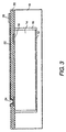
- FIGs. 1-5 are views showing steps in a process for applying a low dielectric constant porous material over a selected surface.
- a semiconductor chip 14 which for example may comprise a GaAs (gallium arsenide) chip having chip pads 16, is attached with an adhesive 12 in a chip well 18 of a milled substrate 10.
- the substrate may comprise any suitable structural material such as, for example, aluminum nitride or beryllium oxide.
- Adhesive 12 may comprise a material such as Ultem polyetherimide resin or silicone epoxy which can withstand high temperature processing.
- a low dielectric constant porous layer 20 is applied over the surfaces of substrate 10 and chip 14.
- the porous layer comprises a porous PTFE material having its pores filled with an additive material.
- the pores have diameters ranging approximately from 0.01 to 5 ⁇ m.
- porous material is preferably a polymer material, other materials such as ceramics and metals can also be used.
- Expanded PTFE is a useful porous layer because it does not dissolve in most of the fabricating chemicals.
- Other examples of potentially useful porous material include polyethylene and polystyrene, for example.
- the selected additive material must be capable of withstanding high processing temperatures and capable of removal after processing by any appropriate process, such as heat or a combination of heat and applied vacuum.
- the additive material may comprise materials such as low melting temperature waxes, anthraquinone (as well as derivatives of anthraquinone such as alizarin), and other sublimable organic solids, such as adipic and other dicarboxylic acids. Some of these additive materials may require vacuum and heat combinations to sublime, whereas others tend to diffuse or evaporate from the material. A short list of sublimable materials can be found in the Handbook of Chemistry and Physics, 60th Ed. pages C-722-723. Many of the listed materials can be readily used with this invention. A combination of several additive materials may be desirable to provide a removable material which can absorb appropriate wavelengths for laser ablation.
- Porous layer 20 is heated to the softening point under pressure and attached to the substrate surface to achieve a bonded laminate.
- the pressure and temperature parameters are chosen so that the additive material does not significantly sublime, diffuse, or evaporate during the attachment.
- the outer porous layer surface can have another coating of the additive material added to refresh the surface after lamination.
- Either an adaptive laser, such as described in aforementioned Eichelberger et al., U.S. Pat. No. 4,835,704, or a mask process is then used to form via openings 24 over selected chip pads 16. as shown in FIG. 3.
- layers such as porous PTFE are not typically laser ablatable using the preferred wavelengths, the process of filling the pores of porous layer 20 with additive material causes the porous layer to be laser ablatable, as further discussed below.
- a layer of electrically conductive material is applied over porous layer 20 and patterned to form a pattern of electrical conductors 22 which, in a preferred embodiment, includes a bonding pad 26.
- the pattern of electrical conductors comprises a buffer layer of metallization such as titanium or chromium covered by a layer of copper which in turn is covered by a second buffer layer. These metals can be patterned with standard photoresist techniques, as discussed in Eichelberger et al., U.S. 4,783,695.
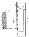
- FIG. 5 is a sectional side view similar to that of FIG. 3.
- FIG. 4 is an enlarged sectional side view along line 4-4' of FIG. 5.
- Substrate 10 can be heated (either with or without vacuum conditions, depending on the additive material) to sublime, diffuse, or evaporate the additive material. Because the additive material does not sublime directly through the pattern of electrical conductors 22, additive material under the pattern of electrical conductors has a longer release path 21a as compared with the release path 21b of additive material not under the pattern of electrical conductors. The longer release path may require a longer heating period.
- Dye molecules such as anthraquinone or alizarin are relatively small molecules and fit between the spaces of the coiled polymer chains which preferably make up the porous layer. When heated above the sublimation temperature, the individual dye molecules, in the gas phase, will vent or pass through these spaces and be released from the porous layer.
- the metal does not significantly protrude into the porous layer and thus has a smooth surface as required for low loss high frequency applications.
- the porous layer may alternatively comprise a polymer without specially formed pores.
- the interdiffusion rate will be slower for such polymers than for porous materials because there will be less volume of free space; however, the sublimable additive material molecules still diffuse through the spaces in polymers without specially formed pores to the surrounding atmosphere.
- the diffusion rate depends on the temperature, pressure, polymer thickness, and permeability of the polymer matrix.
- UV ultraviolet
- UV light acts to scission the material and thus create smaller molecules which can move easily and pass out of the porous materials.
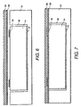
- FIGs. 6-9 are views showing steps in a process for applying a low dielectric constant porous layer similar to the process steps shown in FIGs. 1-5 with the addition of an amorphous adhesive 28 having a low dielectric constant, such as available from DuPont under the name AF 1600 or 2400 Teflon polytetrafluoroethylene, that maintains excellent adhesion to the porous layer after the additive material is removed.
- an amorphous adhesive 28 having a low dielectric constant such as available from DuPont under the name AF 1600 or 2400 Teflon polytetrafluoroethylene, that maintains excellent adhesion to the porous layer after the additive material is removed.
- Another potentially useful adhesive with a low dielectric constant is polyphenylene oxide.
- These low dielectric adhesives are preferably doped with an ultraviolet light absorbing dye as discussed in aforementioned Cole et al., U.S. Patent No. 5,169,678.
- porous layer 20 is immersed and soaked in the additive material which is dissolved in a solvent.
- lon implantation, pressure, or a combination of pressure and heat can be used to Increase the permeation of the additive material throughout the porous layer.
- adhesive 28 is either applied to porous layer 20 or applied to the substrate surface directly. It is helpful to position the additive material in the pores of the porous layer prior to the application and lamination of the porous layer to the substrate surface to prevent the adhesive from wicking or protruding into the pores. Thus the removal of the additive material from the porous layer can be accomplished while maintaining sufficient adhesion of the porous layer to the surface.
- FIGs. 7-9 illustrate views of process steps similar to those of FIGs. 2, 3, and 5, respectively, but do not require as much heat to obtain adhesion of the porous layer to the desired surface.
- AF Teflon polytetrafluoroethylene is used as an adhesive
- the porous layer can attain adequate adhesion to substrate and chip surfaces in the temperature range of 225 °C - 250 °C.
- the step of forming a via opening 24 through porous layer 20 includes forming a corresponding via through adhesive 28.
- the addition of the thin adhesive 28 increases the dielectric constant above the surface because dielectric constants generally act in series and are proportional to the relative thicknesses of the adjacent materials. When the porous layer is much thicker than the adhesive, however, the dielectric constant can approach that of the porous layer and be suitably low.
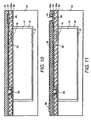
- FIGs. 10-11 are views showing steps in a process for applying multiple low dielectric constant porous layers.
- a second additive filled porous layer 30 is applied with a second adhesive 32 to the outer surface of porous layer 20a of the structure shown in FIG. 9.
- the second porous layer and all subsequent layers can be processed as described with respect to FIGs. 7-9 above by forming a via opening 34 extending to a portion of the pattern of electrical conductors 22, applying a second pattern of electrical conductors 36, and removing the additive material to result in the structure shown in FIG. 11.
- the second adhesive is thin and therefore does not fill the lower vias 24, thus providing an air dielectric constant (about 1) in the metallized via areas.
- the porous layers and adhesives all comprise polytetrafluoroethylene.
- This embodiment uses two different DuPont AF Teflon polytetrafluoroethylene materials such as AF 1600 for adhesives 28 and 32 and AF 2400 for porous layers 20 and 30. These two materials have sufficiently different melting points so that when AF 2400 is a solid the AF 1600 can melt and function as a bonding glue.
- AF Teflon polytetrafluoroethylene materials can have various sublimable materials added that will enable 248-365 nm laser ablation and that can be subsequently be removed by heat or heat and vacuum conditions.
- additive materials include the above-discussed low melting temperature waxes, anthraquinone and its derivatives, and other sublimable organic solids.
- additive materials enables a material that is optical transparent to approximately 200 nm to be laser processable at more conventional laser frequencies such as pulsed excimer lasers at frequencies of 248 nm, 266 nm, 308 nm, and 351 nm, and ion argon or krypton lasers at frequencies of at 350-365 nm and 325 nm, respectively, and subsequently be removed.
- pulsed excimer lasers at frequencies of 248 nm, 266 nm, 308 nm, and 351 nm
- ion argon or krypton lasers at frequencies of at 350-365 nm and 325 nm, respectively, and subsequently be removed.
- the AF Teflon polytetrafluoroethylene layers will release the additive material easily because the materials can be heated near the Tg (glass transition temperature) where the additive material is passed by permeation through the softened material with ease. This process is time, thickness, temperature, and pressure dependent.
- An AF 2400 Teflon polytetrafluoroethylene porous layer can be film cast onto a release plate and an AF 1600 Teflon polytetrafluoroethylene adhesive material can be applied over the top of the porous layer without cracking it, enabling a composite structure that can then be laminated to a PC board or MCM structure.
- This embodiment can be used to reduce the impedance loading which occurs when using high dielectric constant materials.
- Some circuit chip manufacturers employ air bridges to obtain low impedance loading on critical areas of GaAs microcircuits. Typically, when these chips are situated in an integrated circuit, any overlying and underlying material must be removed in the area of the air bridges for optimal performance. This invention may reduce the need to remove material and thus enable new chip interconnection structures to be fabricated.
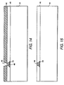
- FIGs. 12-16 are views showing steps in a doping process for enabling laser ablation of low dielectric constant porous layer 40.
- the porous layer is first applied to a substrate 10 surface, as discussed with respect to FIG. 2, but without the additive material.
- a laser ablatable mask material 42 such as Kapton polyimide for example, is deposited over the outer surface of the porous layer.
- a via opening 46 over a portion of an electrical conductor 44 is formed in the mask material revealing the porous layer, as shown in FIG. 12.
- the via is preferably formed with an argon laser, but can also be formed using other conventional methods such as plasma or reactive ion etching, for example.
- the additive material can be supplied to porous layer 40 in a pressure vessel 50 through a pressure port 52 using a heat source 54.
- the dopant may comprise a light absorbing dye such as discussed in aforementioned Cole et al., U.S. Patent No. 5,169.678.
- Mask material 42 limits doping or diffusion to the localized areas 48 where the vias have been formed to cause permeation of the of the additive material for enabling laser ablation at CW argon ion laser frequencies. If desired, mask material 42 can also be applied over the side edges of the porous layer to prevent doping of the side edges. Slight doping which may occur along the edges of the porous layer, however, does not present any problems.
- FIG. 14 illustrates a doped region ready for laser processing.
- the mask material can be removed, as shown in FIG. 15, and a laser can be used to produce vias in the porous layer where the additive material was doped because of the selective absorption of the excimer laser energy in the doped via areas.
- any remaining dopant material can be removed by a process such as sublimation, for example, leaving the material again transparent to the excimer laser's light energy, as shown by via 56 in FIG. 16.
- FIGs. 17-19 are views showing steps in a process for forming a low dielectric constant printed circuit board.
- a porous layer 110 is filled with additive material as described with respect to FIG. 2.
- the porous layer is preferably coated on both sides with thin layers of an adhesive material 112a and 112b, comprising a material such as AF 1600 or 2400 Teflon polytetrafluoroethylene, which in turn are coated with respective layers of metallization 114a and 114b, comprising a material such as copper, as shown in FIG. 17.
- DuPont FEP or PFA Teflon polytetrafluoroethylene is applied with a pinch roll laminator such as used in PC board processing.
- holes 116 are punched or drilled through the porous material, adhesive, and metallization, and, as shown in FIG. 19 , the layers of metallization are patterned to form metallization lines on the board.
- the patterning is performed using a layer of photoresist (not shown) which is removed after patterning. If desired, any adhesive left exposed after the patterning of the metallization layer can be removed by RIE (reactive ion etching).
- RIE reactive ion etching
Landscapes
- Engineering & Computer Science (AREA)
- Microelectronics & Electronic Packaging (AREA)
- Physics & Mathematics (AREA)
- Optics & Photonics (AREA)
- Manufacturing & Machinery (AREA)
- Laminated Bodies (AREA)
- Manufacturing Of Printed Wiring (AREA)
- Production Of Multi-Layered Print Wiring Board (AREA)
- Printing Elements For Providing Electric Connections Between Printed Circuits (AREA)
Abstract
Description
- This invention relates generally to low dielectric constant porous materials and, more particularly, to a process for using porous layers in printed circuit boards and over electronic circuits and supporting substrates.
- Electronic circuits have inherent limitations in high frequency applications. For example, capacitive loading is increased at higher frequencies because capacitive reactance is directly proportional to frequency. In high frequency circuits capacitive loading becomes so high that a semiconductor chip cannot drive the low reactive impedance. Because these high frequency circuits have historically been power inefficient, their usefulness in airborne and satellite applications is limited.
- Foam cored cable technology has been used for years in attempts to reduce capacitive loading of electronic signals. Porous polytetrafluoroethylene (PTFE) materials such as Gortex™ (Gortex is a trademark of W.L. Gore & Associates, Inc., of Newark, DE) have excellent low dielectric constant properties, but unfortunately they absorb process chemicals in their pores during MCM (multichip module) or PC (printed circuit) board processing that cannot be removed. Additionally, the fact that the porous material deforms during pressurized processing destroys its porous properties, and therefore the deformed material does not provide the desired consistent low dielectric constant.
- In microwave circuit chip structures, certain electrical conductor paths in sensitive areas of the chip circuitry require a dielectric constant close to that of air (1) to work properly in these areas. Chip manufacturers fabricate air bridges to provide the low dielectric constant. These sensitive air bridge structures create processing challenges for both the manufacturer and the end user. Even Teflon polytetrafluoroethylene (Teflon is a trademark of E.I. DuPont de Nemours and Co.), which typically has a dielectric constant between 1.9 and 2.0, can create too much of an impedance loading effect at microwave frequencies.
- The DuPont Teflon polytetrafluoroethylene line of materials has intrinsically low dielectric constants and has the necessary high temperature stability for most industrial and military uses. As described in Gore, U.S. Patent No. 3,962,153, and Gore, U.S. Patent No. 4,096,227, Gortex material is a Teflon PTFE-based material that is filled with micro-pores that create a foam-like cloth material. Porous PTFE material is generally used in clothes to simultaneously provide warmth and allow perspiration and moisture vapors to vent through its pores. Porous PTFE material is alternatively sold as a filled porous PTFE material. Filling the pores with a material such as an acrylate glue enables use of the material as a laminant film; however, this causes the resultant dielectric constant to degrade and limits the material's usefulness at high frequencies. A filled porous material is disclosed in U.S. Patent No. 5,034,801. Unfilled porous PTFE material is an excellent candidate for high frequency circuits because the dielectric constant can be significantly less than that found in other materials. However, in laminant applications and processing, the pores can collapse under pressure and/or be filled witn processing materials during fabrication which cannot be easily removed.
- Ceramic foam materials are discussed, for example, in "Giants in advanced ceramics," Ceramic Industry, vol. 141, 47 (August 1993), and Te-Kao Wu, "Dielectric properties measurement of substrate and support materials," Microwave and Optical Technology Letters, vol. 3, 283-286 (August 1990). These materials, however, are inflexible and not fabricated in large area sections. Because the ceramic foam materials are inflexible, they can be used as substrates but cannot be used in overlay technologies that are not perfectly flat. Because ceramic foam materials are fragile, they are typically not capable of withstanding PC board lamination processing in their intrinsic state. Furthermore, ceramic foam materials can be filled with processing materials which degrade their low dielectric constant.
- Another problem common to both porous PTFE material and ceramic foam material is that if the porous/foam material is to be used in any process in which a metallization layer is applied over the material, the metal tends to extend into the pores and it is thus difficult to achieve a smooth and continuous metal surface for use in high frequency applications where skin-effect related losses are of importance.
- Few intrinsically low dielectric constant materials can withstand the high temperatures in commercial and military processing. Most of the low dielectric constant materials that can withstand higher temperatures are only absorptive below the 200 nanometer wavelength region of the light spectrum, and thus it is nearly impossible to process those materials using ion argon and other CW (continuous wave) lasers.
- Polymer materials in high frequency circuits are preferably laser ablatable by ultraviolet light in order to form the via openings through which different layers of metallization are connected. Laser processing (ablation, photoresist exposure, etc.) is normally done with several passes of the laser beam with a power ranging from 0.5 to 2.0 watts, with a preferred maximum power level being about 1.5 watts. Thus, when a dielectric layer is characterized as being laser ablatable, it means that such layer can be totally removed by progressive passes of a laser beam of this power level, and when it is characterized as not being laser ablatable, it means that a layer is not completely removed by progressive passes of such a laser beam. One method of adaptive laser ablation is discussed in Eichelberger et al., U.S. Patent No. 4,835,704. Most polytetrafluoroethylene materials are not laser ablatable and generally do not easily adhere to other materials. A method of modifying the ultraviolet absorption characteristics of a polymer material with the addition of an ultraviolet absorbing dye is discussed is Cole et al., U.S. Patent No. 5,169,678.
- To minimize the complexity and cost of equipment for fabricating high density interconnect structures, it is considered desirable to be able to do all laser processing at a single frequency in order that only a single laser is required. Accordingly, preferred materials are those which can be processed at a laser frequency of 351 nm. This frequency was selected in accordance with the characteristics of desirable dielectric layers such as Kapton™ polyimide (Kapton is a trademark of E.I. DuPont de Nemours and Co.) and the fact that there are commercial photoresists which can be processed at this frequency. Ultem™ polyetherimide resin (Ultem is a registered trademark of General Electric Co.) has been used as an adhesive layer in this high density interconnect structure for bonding Kapton polyimide to the underlying structures. The Ultem polyetherimide resin is laser ablatable at 351 nm.
- PC boards typically have dielectric constants ranging from 2 through 5, and nonporous ceramics can have dielectric constants as high as 9. It would be desirable to have a low dielectric constant PC board material for use in high frequency and high speed electronics.
- The present invention aims to provide a new material and method of manufacturing high frequency and high speed electronic circuits with low power capabilities.
- This invention also aims to provide a method for processing low dielectric constant porous materials which does not leave process chemicals behind in the porous materials.
- Preferably there is provided a method for adding materials to the pores of the porous material that allow laser processing at an ultra-violet (UV) wavelength of about 350 nanometers (nm).
- This invention may also provide low dielectric constant polymer and ceramic PC boards.
- This invention modifies a low dielectric constant polymeric porous material, such as porous PTFE material, which has a dielectric constant of approximately 1.2-1.3, by filling the material's pores with a sublimable (or otherwise removable) material that prevents deformation and enables laser processing during high speed circuit fabrication. The term "low dielectric constant" is intended to mean a dielectric constant as close to 1 as possible and not greater than about 2. After processing, the filler material is removed, and the original porous material is left with the intrinsically low dielectric constant. The process, which enables foam-like materials to be laminated and laser machined without the use of solvents or other chemical processing, can be used in PC boards, MCM modules, and anywhere else low dielectric constant surfaces are desired.
- Porous PTFE material is approximately 70% air and is generally made by stretching PTFE to cause approximately nine billion holes per square inch to be distributed evenly throughout its volume. This porous structure is composed of mostly air and can readily be filled with a sublimable material. The resulting porous material can be used as a low dielectric constant material in the manufacture of high frequency circuits and can reduce the need for laser ablation of material situated over air bridge structures and other microwave structures and devices.
- Briefly, in accordance with a preferred embodiment of the invention, a method for applying a low dielectric constant material over a substrate comprises dispersing an additive material in a low dielectric constant layer; attaching the layer to a surface of the substrate; and removing the additive material from the layer. In one embodiment the low dielectric constant layer is a porous layer comprising polytetrafluoroethylene. The step of removing the additive material from the layer comprises subliming, evaporating, and/or diffusing away the additive material. The substrate can support a circuit chip having chip pads on a connection surface. In this embodiment the step of attaching the porous layer to the surface of the substrate includes attaching the porous layer to the connection surface of the circuit chip, and further steps include forming at least one via in the porous layer extending to at least one of the chip pads and applying a pattern of electrically conductive material over the porous layer extending into the at least one via.
- In accordance with another preferred embodiment of the invention, a method for applying and ablating a low dielectric constant material over a substrate comprises attaching a low dielectric constant polymer layer to a surface of the substrate; applying mask material over the polymer layer; forming a via in the mask material extending through to the polymer layer; diffusing an additive material in a region of the polymer layer through the via in the mask material; removing the mask material; and ablating at least some of the polymer layer in the region where the additive material was diffused.
- In accordance with another preferred embodiment of the invention, a method for fabricating a low dielectric constant printed circuit board comprises dispersing an additive material in a low dielectric constant layer; applying an adhesive over at least one side of the low dielectric constant layer; applying a metallization layer over the adhesive; providing a plurality of holes through the low dielectric constant layer, the adhesive, and the metallization layer; patterning the metallization layer; and removing the additive material from the low dielectric constant layer.
- The features of the invention believed to be novel are set forth with particularity in the appended claims. The invention itself, however, both as to organization and method of operation, together with further objects and advantages thereof, may best be understood by reference to the following description taken in conjunction with the accompanying drawings, where like numerals represent like components, in which:
- FIGs. 1-5 are views showing steps in a process for applying a low dielectric constant porous layer over a selected surface;
- FIGs. 6-9 are views showing steps in another process for applying a low dielectric constant porous layer over a selected surface;
- FIGs. 10-11 are views showing steps in a process for applying multiple low dielectric constant porous layers;
- FIGs. 12-16 are views showing steps in a process for enabling laser ablation of low dielectric constant porous material; and
- FIGs. 17-19 are views showing steps in a process for forming a low dielectric constant printed circuit board.
-
- FIGs. 1-5 are views showing steps in a process for applying a low dielectric constant porous material over a selected surface. In the view of FIG. 1, a
semiconductor chip 14, which for example may comprise a GaAs (gallium arsenide) chip havingchip pads 16, is attached with an adhesive 12 in a chip well 18 of a milledsubstrate 10. The substrate may comprise any suitable structural material such as, for example, aluminum nitride or beryllium oxide.Adhesive 12 may comprise a material such as Ultem polyetherimide resin or silicone epoxy which can withstand high temperature processing. - As shown in FIG. 2, a low dielectric constant
porous layer 20 is applied over the surfaces ofsubstrate 10 andchip 14. In one embodiment the porous layer comprises a porous PTFE material having its pores filled with an additive material. In one example, the pores have diameters ranging approximately from 0.01 to 5 µm. - Although the porous material is preferably a polymer material, other materials such as ceramics and metals can also be used. Expanded PTFE is a useful porous layer because it does not dissolve in most of the fabricating chemicals. Other examples of potentially useful porous material include polyethylene and polystyrene, for example.
- The selected additive material must be capable of withstanding high processing temperatures and capable of removal after processing by any appropriate process, such as heat or a combination of heat and applied vacuum.
- For example, the additive material may comprise materials such as low melting temperature waxes, anthraquinone (as well as derivatives of anthraquinone such as alizarin), and other sublimable organic solids, such as adipic and other dicarboxylic acids. Some of these additive materials may require vacuum and heat combinations to sublime, whereas others tend to diffuse or evaporate from the material. A short list of sublimable materials can be found in the Handbook of Chemistry and Physics, 60th Ed. pages C-722-723. Many of the listed materials can be readily used with this invention. A combination of several additive materials may be desirable to provide a removable material which can absorb appropriate wavelengths for laser ablation.
-
Porous layer 20 is heated to the softening point under pressure and attached to the substrate surface to achieve a bonded laminate. The pressure and temperature parameters are chosen so that the additive material does not significantly sublime, diffuse, or evaporate during the attachment. The outer porous layer surface can have another coating of the additive material added to refresh the surface after lamination. - Either an adaptive laser, such as described in aforementioned Eichelberger et al., U.S. Pat. No. 4,835,704, or a mask process is then used to form via
openings 24 over selectedchip pads 16. as shown in FIG. 3. Although, layers such as porous PTFE are not typically laser ablatable using the preferred wavelengths, the process of filling the pores ofporous layer 20 with additive material causes the porous layer to be laser ablatable, as further discussed below. - After the vias are cleaned, a layer of electrically conductive material is applied over
porous layer 20 and patterned to form a pattern ofelectrical conductors 22 which, in a preferred embodiment, includes abonding pad 26. In one embodiment the pattern of electrical conductors comprises a buffer layer of metallization such as titanium or chromium covered by a layer of copper which in turn is covered by a second buffer layer. These metals can be patterned with standard photoresist techniques, as discussed in Eichelberger et al., U.S. 4,783,695. - As shown in FIGs. 4 and 5, the additive material is then removed from from the additive-filled
porous layer 20 to form an additive-freeporous layer 20a. FIG. 5 is a sectional side view similar to that of FIG. 3. FIG. 4 is an enlarged sectional side view along line 4-4' of FIG. 5.Substrate 10 can be heated (either with or without vacuum conditions, depending on the additive material) to sublime, diffuse, or evaporate the additive material. Because the additive material does not sublime directly through the pattern ofelectrical conductors 22, additive material under the pattern of electrical conductors has alonger release path 21a as compared with therelease path 21b of additive material not under the pattern of electrical conductors. The longer release path may require a longer heating period. - The removal of additive material dyes dissolved or dispersed in a polymer matrix occurs through a mechanism of interdiffusion. Dye molecules such as anthraquinone or alizarin are relatively small molecules and fit between the spaces of the coiled polymer chains which preferably make up the porous layer. When heated above the sublimation temperature, the individual dye molecules, in the gas phase, will vent or pass through these spaces and be released from the porous layer.
- Because the additive material is removed after the application of the pattern of electrical conductors, the metal does not significantly protrude into the porous layer and thus has a smooth surface as required for low loss high frequency applications.
- Although this invention has been discussed with the concept of using a porous material, the porous layer may alternatively comprise a polymer without specially formed pores. The interdiffusion rate will be slower for such polymers than for porous materials because there will be less volume of free space; however, the sublimable additive material molecules still diffuse through the spaces in polymers without specially formed pores to the surrounding atmosphere. The diffusion rate depends on the temperature, pressure, polymer thickness, and permeability of the polymer matrix.
- Certain light frequencies, such as UV (ultraviolet), aid in the decomposition of the additive material. UV light acts to scission the material and thus create smaller molecules which can move easily and pass out of the porous materials.
- FIGs. 6-9 are views showing steps in a process for applying a low dielectric constant porous layer similar to the process steps shown in FIGs. 1-5 with the addition of an
amorphous adhesive 28 having a low dielectric constant, such as available from DuPont under the name AF 1600 or 2400 Teflon polytetrafluoroethylene, that maintains excellent adhesion to the porous layer after the additive material is removed. Another potentially useful adhesive with a low dielectric constant is polyphenylene oxide. These low dielectric adhesives are preferably doped with an ultraviolet light absorbing dye as discussed in aforementioned Cole et al., U.S. Patent No. 5,169,678. - In this embodiment,
porous layer 20 is immersed and soaked in the additive material which is dissolved in a solvent. lon implantation, pressure, or a combination of pressure and heat can be used to Increase the permeation of the additive material throughout the porous layer. - After the porous layer and additive material have dried, adhesive 28 is either applied to
porous layer 20 or applied to the substrate surface directly. It is helpful to position the additive material in the pores of the porous layer prior to the application and lamination of the porous layer to the substrate surface to prevent the adhesive from wicking or protruding into the pores. Thus the removal of the additive material from the porous layer can be accomplished while maintaining sufficient adhesion of the porous layer to the surface. - FIGs. 7-9 illustrate views of process steps similar to those of FIGs. 2, 3, and 5, respectively, but do not require as much heat to obtain adhesion of the porous layer to the desired surface. When AF Teflon polytetrafluoroethylene is used as an adhesive, the porous layer can attain adequate adhesion to substrate and chip surfaces in the temperature range of 225 °C - 250 °C. The step of forming a via
opening 24 throughporous layer 20 includes forming a corresponding via throughadhesive 28. - The addition of the thin adhesive 28 increases the dielectric constant above the surface because dielectric constants generally act in series and are proportional to the relative thicknesses of the adjacent materials. When the porous layer is much thicker than the adhesive, however, the dielectric constant can approach that of the porous layer and be suitably low.
- FIGs. 10-11 are views showing steps in a process for applying multiple low dielectric constant porous layers. in FIG. 10, a second additive filled
porous layer 30 is applied with a second adhesive 32 to the outer surface ofporous layer 20a of the structure shown in FIG. 9. The second porous layer and all subsequent layers can be processed as described with respect to FIGs. 7-9 above by forming a viaopening 34 extending to a portion of the pattern ofelectrical conductors 22, applying a second pattern ofelectrical conductors 36, and removing the additive material to result in the structure shown in FIG. 11. The second adhesive is thin and therefore does not fill thelower vias 24, thus providing an air dielectric constant (about 1) in the metallized via areas. - In a multilayer structure, not all the layers need be applied as additive material filled porous layers. Other materials, such as Kapton polyimide (Kapton is a trademark of E.I. DuPont de Nemours and Co.), for example, can be used in combination with porous layers. The high speed or high frequency porous layers need only be placed where desirable.
- Instead of removing the additive material after each layer is applied, several layers can be processed before attempting to remove the additive material. When removing additive material from several layers simultaneously a longer heating period will be required than the period for removing additive material from a single layer.
- In one embodiment, the porous layers and adhesives all comprise polytetrafluoroethylene. This embodiment uses two different DuPont AF Teflon polytetrafluoroethylene materials such as AF 1600 for
adhesives porous layers - AF Teflon polytetrafluoroethylene materials can have various sublimable materials added that will enable 248-365 nm laser ablation and that can be subsequently be removed by heat or heat and vacuum conditions. Several examples of such additive materials include the above-discussed low melting temperature waxes, anthraquinone and its derivatives, and other sublimable organic solids. Using these additive materials enables a material that is optical transparent to approximately 200 nm to be laser processable at more conventional laser frequencies such as pulsed excimer lasers at frequencies of 248 nm, 266 nm, 308 nm, and 351 nm, and ion argon or krypton lasers at frequencies of at 350-365 nm and 325 nm, respectively, and subsequently be removed.
- The AF Teflon polytetrafluoroethylene layers will release the additive material easily because the materials can be heated near the Tg (glass transition temperature) where the additive material is passed by permeation through the softened material with ease. This process is time, thickness, temperature, and pressure dependent.
- An AF 2400 Teflon polytetrafluoroethylene porous layer can be film cast onto a release plate and an AF 1600 Teflon polytetrafluoroethylene adhesive material can be applied over the top of the porous layer without cracking it, enabling a composite structure that can then be laminated to a PC board or MCM structure.
- This embodiment can be used to reduce the impedance loading which occurs when using high dielectric constant materials. Some circuit chip manufacturers employ air bridges to obtain low impedance loading on critical areas of GaAs microcircuits. Typically, when these chips are situated in an integrated circuit, any overlying and underlying material must be removed in the area of the air bridges for optimal performance. This invention may reduce the need to remove material and thus enable new chip interconnection structures to be fabricated.
- FIGs. 12-16 are views showing steps in a doping process for enabling laser ablation of low dielectric constant
porous layer 40. The porous layer is first applied to asubstrate 10 surface, as discussed with respect to FIG. 2, but without the additive material. Then, in a preferred embodiment, a laserablatable mask material 42, such as Kapton polyimide for example, is deposited over the outer surface of the porous layer. A viaopening 46 over a portion of anelectrical conductor 44 is formed in the mask material revealing the porous layer, as shown in FIG. 12. The via is preferably formed with an argon laser, but can also be formed using other conventional methods such as plasma or reactive ion etching, for example. - As shown in FIG. 13, the additive material can be supplied to
porous layer 40 in apressure vessel 50 through apressure port 52 using aheat source 54. The dopant may comprise a light absorbing dye such as discussed in aforementioned Cole et al., U.S. Patent No. 5,169.678.Mask material 42 limits doping or diffusion to thelocalized areas 48 where the vias have been formed to cause permeation of the of the additive material for enabling laser ablation at CW argon ion laser frequencies. If desired,mask material 42 can also be applied over the side edges of the porous layer to prevent doping of the side edges. Slight doping which may occur along the edges of the porous layer, however, does not present any problems. - FIG. 14 illustrates a doped region ready for laser processing. Once the desired via areas are doped with the additive material to enable localized laser ablation, the mask material can be removed, as shown in FIG. 15, and a laser can be used to produce vias in the porous layer where the additive material was doped because of the selective absorption of the excimer laser energy in the doped via areas. After via formation, any remaining dopant material can be removed by a process such as sublimation, for example, leaving the material again transparent to the excimer laser's light energy, as shown by via 56 in FIG. 16.
- FIGs. 17-19 are views showing steps in a process for forming a low dielectric constant printed circuit board. First, a
porous layer 110 is filled with additive material as described with respect to FIG. 2. The porous layer is preferably coated on both sides with thin layers of anadhesive material metallization - Next, as shown in FIG. 18, holes 116 are punched or drilled through the porous material, adhesive, and metallization, and, as shown in FIG. 19, the layers of metallization are patterned to form metallization lines on the board. In one embodiment, the patterning is performed using a layer of photoresist (not shown) which is removed after patterning. If desired, any adhesive left exposed after the patterning of the metallization layer can be removed by RIE (reactive ion etching). After the metallization lines are fabricated, electronic components can be inserted in the board, and removal of the additive material is accomplished by sublimation, evaporation, and/or diffusion, as discussed above.
- While only certain preferred features of the invention have been illustrated and described herein, many modifications and changes will occur to those skilled in the art.
Claims (20)
- A method for applying a porous low dielectric constant material layer (20) having a dielectric constant no greater than 2 over a substrate (10), comprising the steps of:dispersing an additive material in the porous low dielectric constant layer, so as to fill pores in the dielectric constant layer with said additive material;attaching the layer (20) to a surface (10) of the substrate; andremoving the additive material from the layer.
- The method of claim 1, wherein the step of removing the additive material from the layer comprises a process selected from the group consisting of sublimation, evaporation, and diffusion.
- The method of claim 2, wherein the additive material is sublimable in the layer.
- The method of claim 2, wherein the layer comprises a material selected from the group consisting of polymers and ceramics.
- The method of claim 2, wherein the substrate (10) supports a circuit chip (14) having chip pads (16) on a connection surface and wherein the step of attaching the layer to the surface of the substrate includes attaching the layer (20) to the connection surface of the circuit chip, and further including, prior to removing the additive material from the layer, the steps of:forming at least one via (24) in the layer extending to at least one of the chip pads (16); andapplying a pattern of electrically conductive material over the layer, the pattern of electrically conductive material extending into the at least one via.
- The method of claim 5, wherein the layer comprises a polymer.
- The method of claim 6, wherein the porous layer comprises a material selected from the group consisting of polytetrafluoroethylene, polethylene, and polystyrene.
- The method of claim 7, wherein the additive material comprises a material selected from the group consisting of wax, anthraquinone, and sublimable organic solids.
- The method of claim 6, wherein the step of attaching the porous layer to the substrate surface includes using an adhesive (28) between the porous layer (20) and the substrate surface (10).
- The method of claim 9, wherein the adhesive comprises an adhesive selected from the group consisting of polytetrafluoroethylene and polyphenylene oxide.
- The method of claim 6, further including, after applying the pattern of electrical conductors (22), the steps of:attaching an additional porous layer (30) having dispersed additional additive material therein to the surface of the porous layer (20a) and the pattern of electrical conductors with an adhesive (32); andforming an additional via (34) in the additional porous layer extending to a portion of the pattern of electrically conductive material (22); andapplying an additional pattern of electrically conductive material (36) over the additional porous layer (30), the additional pattern of electrically conductive material extending into the additional via (34); andremoving the additional additive material from the additional porous layer (30).
- The method of claim 11, wherein the steps of removing the additive material from the porous layer and removing the additional additive material from the additional porous layer occur simultaneously.
- The method of claim 11, wherein the porous layer (20) and additional porous layer (30) comprise a first polytetrafluoroethylene material and the adhesive comprises a second polytetrafluoroethylene material, the second polytetrafluoroethylene material having a lower melting point than the first polytetrafluoroethylene material.
- The method of claim 1, wherein the step of attaching the porous layer (20) to the surface of the substrate (10) includes applying an adhesive (28) between the porous layer (20) and the surface, and wherein the porous layer comprises a first polytetrafluoroethylene material and the adhesive comprises a second polytetrafluoroethylene material, the second polytetrafluoroethylene material having a lower melting point than the first polytetrafluoroethylene material.
- The method of claim 5, wherein the substrate is a circuit board and the method further comprises the steps of:wherein the steps a) - c) are taken after the low dielectric constant porous polymer layer is attached to the substrate and before the additive material is removed from the low dielectric constant porous polymer layer.a) providing holes (116) through the low dielectric constant porous polymer layer;b) applying a metallization layer (114a) over surfaces of the low dielectric constant porous polymer layer and surfaces of the holes;c) patterning the metallization layer; and
- The method of claim 15, further including, prior to applying the metallization layer, applying an adhesive (112a) over the surfaces of the low dielectric constant porous polymer layer.
- The method of claim 16, wherein the step of removing the additive material from the low dielectric constant porous polymer layer comprises a process selected from the group consisting of sublimation, evaporation, and diffusion.
- The method of claim 16, wherein the low dielectric constant porous polymer layer comprises a material selected from the group consisting of polytetrafluoroethylene, polyethylene, and polystyrene.
- The method of claim 18, wherein the additive material comprises a material selected from the group consisting of wax, anthraquinone, and sublimable organic solids.
- The method of claim 16, wherein the step of applying a metallization layer over surfaces of the low dielectric constant porous polymer layer and surfaces of the holes includes providing inner layers of metallization over the surfaces of the low dielectric constant porous polymer layer prior to providing holes and providing outer layers of metallization over the surfaces of the holes after providing holes, the metallization layer comprising the inner and outer layers of metallization.
Priority Applications (1)
| Application Number | Priority Date | Filing Date | Title |
|---|---|---|---|
| EP04020818A EP1484949B1 (en) | 1994-05-23 | 1995-05-15 | Processing low dielectric constant materials for high speed electronics |
Applications Claiming Priority (3)
| Application Number | Priority Date | Filing Date | Title |
|---|---|---|---|
| US247820 | 1988-10-24 | ||
| US08/247,820 US5449427A (en) | 1994-05-23 | 1994-05-23 | Processing low dielectric constant materials for high speed electronics |
| PCT/US1995/005983 WO1995032604A1 (en) | 1994-05-23 | 1995-05-15 | Processing low dielectric constant materials for high speed electronics |
Related Child Applications (1)
| Application Number | Title | Priority Date | Filing Date |
|---|---|---|---|
| EP04020818A Division EP1484949B1 (en) | 1994-05-23 | 1995-05-15 | Processing low dielectric constant materials for high speed electronics |
Publications (2)
| Publication Number | Publication Date |
|---|---|
| EP0710430A1 EP0710430A1 (en) | 1996-05-08 |
| EP0710430B1 true EP0710430B1 (en) | 2004-11-24 |
Family
ID=22936514
Family Applications (2)
| Application Number | Title | Priority Date | Filing Date |
|---|---|---|---|
| EP95920427A Expired - Lifetime EP0710430B1 (en) | 1994-05-23 | 1995-05-15 | Processing low dielectric constant materials for high speed electronics |
| EP04020818A Expired - Lifetime EP1484949B1 (en) | 1994-05-23 | 1995-05-15 | Processing low dielectric constant materials for high speed electronics |
Family Applications After (1)
| Application Number | Title | Priority Date | Filing Date |
|---|---|---|---|
| EP04020818A Expired - Lifetime EP1484949B1 (en) | 1994-05-23 | 1995-05-15 | Processing low dielectric constant materials for high speed electronics |
Country Status (6)
| Country | Link |
|---|---|
| US (3) | US5449427A (en) |
| EP (2) | EP0710430B1 (en) |
| JP (2) | JP3769297B2 (en) |
| CA (1) | CA2163627A1 (en) |
| DE (2) | DE69533789T2 (en) |
| WO (1) | WO1995032604A1 (en) |
Families Citing this family (70)
| Publication number | Priority date | Publication date | Assignee | Title |
|---|---|---|---|---|
| US5785787A (en) * | 1994-05-23 | 1998-07-28 | General Electric Company | Processing low dielectric constant materials for high speed electronics |
| US5889104A (en) * | 1996-01-11 | 1999-03-30 | W. L. Gore & Associates, Inc. | Low dielectric constant material for use as an insulation element in an electronic device |
| GB9610689D0 (en) * | 1996-05-22 | 1996-07-31 | Int Computers Ltd | Flip chip attachment |
| JP3305211B2 (en) * | 1996-09-10 | 2002-07-22 | 松下電器産業株式会社 | Semiconductor device and manufacturing method thereof |
| US5938452A (en) * | 1996-12-23 | 1999-08-17 | General Electric Company | Flexible interface structures for electronic devices |
| US5900674A (en) * | 1996-12-23 | 1999-05-04 | General Electric Company | Interface structures for electronic devices |
| US6303488B1 (en) * | 1997-02-12 | 2001-10-16 | Micron Technology, Inc. | Semiconductor processing methods of forming openings to devices and substrates, exposing material from which photoresist cannot be substantially selectively removed |
| EP0972303A1 (en) * | 1997-04-03 | 2000-01-19 | W.L. Gore & Associates, Inc. | Low dielectric constant material with improved dielectric strength |
| US6077792A (en) * | 1997-07-14 | 2000-06-20 | Micron Technology, Inc. | Method of forming foamed polymeric material for an integrated circuit |
| SE510487C2 (en) * | 1997-09-17 | 1999-05-31 | Ericsson Telefon Ab L M | Multilayer PCB |
| JP3661444B2 (en) * | 1998-10-28 | 2005-06-15 | 株式会社ルネサステクノロジ | Semiconductor device, semiconductor wafer, semiconductor module, and semiconductor device manufacturing method |
| JP2002530505A (en) | 1998-11-24 | 2002-09-17 | ザ ダウ ケミカル カンパニー | Composition containing crosslinkable matrix precursor and porogen, and porous matrix produced therefrom |
| US6495468B2 (en) | 1998-12-22 | 2002-12-17 | Micron Technology, Inc. | Laser ablative removal of photoresist |
| US6466113B1 (en) * | 1999-01-22 | 2002-10-15 | Spectrian Corporation | Multi-layer RF printed circuit architecture with low-inductance interconnection and low thermal resistance for wide-lead power devices |
| US7276788B1 (en) | 1999-08-25 | 2007-10-02 | Micron Technology, Inc. | Hydrophobic foamed insulators for high density circuits |
| US6677209B2 (en) | 2000-02-14 | 2004-01-13 | Micron Technology, Inc. | Low dielectric constant STI with SOI devices |
| US6413827B2 (en) | 2000-02-14 | 2002-07-02 | Paul A. Farrar | Low dielectric constant shallow trench isolation |
| US6890847B1 (en) | 2000-02-22 | 2005-05-10 | Micron Technology, Inc. | Polynorbornene foam insulation for integrated circuits |
| US6483044B1 (en) | 2000-08-23 | 2002-11-19 | Micron Technology, Inc. | Interconnecting substrates for electrical coupling of microelectronic components |
| US6838760B1 (en) | 2000-08-28 | 2005-01-04 | Micron Technology, Inc. | Packaged microelectronic devices with interconnecting units |
| US6703324B2 (en) * | 2000-12-21 | 2004-03-09 | Intel Corporation | Mechanically reinforced highly porous low dielectric constant films |
| JP3887175B2 (en) * | 2001-02-02 | 2007-02-28 | 沖電気工業株式会社 | Semiconductor device and manufacturing method thereof |
| US6303524B1 (en) | 2001-02-20 | 2001-10-16 | Mattson Thermal Products Inc. | High temperature short time curing of low dielectric constant materials using rapid thermal processing techniques |
| DE10109786A1 (en) * | 2001-02-28 | 2002-12-12 | Fractal Ag | Process for the production of printed circuit boards |
| TW544882B (en) | 2001-12-31 | 2003-08-01 | Megic Corp | Chip package structure and process thereof |
| TW584950B (en) | 2001-12-31 | 2004-04-21 | Megic Corp | Chip packaging structure and process thereof |
| TW503496B (en) | 2001-12-31 | 2002-09-21 | Megic Corp | Chip packaging structure and manufacturing process of the same |
| US6673698B1 (en) | 2002-01-19 | 2004-01-06 | Megic Corporation | Thin film semiconductor package utilizing a glass substrate with composite polymer/metal interconnect layers |
| US6964881B2 (en) * | 2002-08-27 | 2005-11-15 | Micron Technology, Inc. | Multi-chip wafer level system packages and methods of forming same |
| US6703114B1 (en) * | 2002-10-17 | 2004-03-09 | Arlon | Laminate structures, methods for production thereof and uses therefor |
| US6905914B1 (en) | 2002-11-08 | 2005-06-14 | Amkor Technology, Inc. | Wafer level package and fabrication method |
| US7723210B2 (en) * | 2002-11-08 | 2010-05-25 | Amkor Technology, Inc. | Direct-write wafer level chip scale package |
| US7192892B2 (en) | 2003-03-04 | 2007-03-20 | Micron Technology, Inc. | Atomic layer deposited dielectric layers |
| DE10335155B4 (en) * | 2003-07-31 | 2006-11-30 | Infineon Technologies Ag | Method for producing an arrangement of an electrical component on a substrate |
| US20050137882A1 (en) * | 2003-12-17 | 2005-06-23 | Cameron Don T. | Method for authenticating goods |
| US7527585B2 (en) * | 2004-07-21 | 2009-05-05 | Illinois Tool Works Inc. | Methods of making reclosable packages for vacuum, pressure and/or liquid containment |
| US7316512B2 (en) * | 2004-07-30 | 2008-01-08 | General Electric Company | Interconnect device |
| JP4380466B2 (en) * | 2004-08-23 | 2009-12-09 | 住友電気工業株式会社 | Perforated porous resin base material and method for producing porous resin base material with inner wall surface of perforation made conductive |
| US7927948B2 (en) | 2005-07-20 | 2011-04-19 | Micron Technology, Inc. | Devices with nanocrystals and methods of formation |
| US7829386B2 (en) * | 2005-08-17 | 2010-11-09 | General Electric Company | Power semiconductor packaging method and structure |
| US7262444B2 (en) * | 2005-08-17 | 2007-08-28 | General Electric Company | Power semiconductor packaging method and structure |
| US7572681B1 (en) | 2005-12-08 | 2009-08-11 | Amkor Technology, Inc. | Embedded electronic component package |
| US8551153B2 (en) * | 2005-12-20 | 2013-10-08 | Cordis Corporation | Prosthesis comprising a coiled stent and method of use thereof |
| WO2007104006A2 (en) * | 2006-03-09 | 2007-09-13 | Imerys Kaolin, Inc. | Large particle, high mineral purity delaminated kaolins and methods of preparing and using same |
| US7902660B1 (en) | 2006-05-24 | 2011-03-08 | Amkor Technology, Inc. | Substrate for semiconductor device and manufacturing method thereof |
| US7524775B2 (en) | 2006-07-13 | 2009-04-28 | Infineon Technologies Ag | Method for producing a dielectric layer for an electronic component |
| TWI322494B (en) * | 2006-10-20 | 2010-03-21 | Ind Tech Res Inst | Electrical package, and contact structure and fabricating method thereof |
| US7833456B2 (en) | 2007-02-23 | 2010-11-16 | Micron Technology, Inc. | Systems and methods for compressing an encapsulant adjacent a semiconductor workpiece |
| MY148660A (en) * | 2007-04-10 | 2013-05-15 | Sumitomo Bakelite Co | Resin composition, prepreg, laminated board, multilayer printed wiring board and semiconductor device |
| JP5140014B2 (en) * | 2009-02-03 | 2013-02-06 | 富士通株式会社 | Manufacturing method of semiconductor device |
| US8796561B1 (en) | 2009-10-05 | 2014-08-05 | Amkor Technology, Inc. | Fan out build up substrate stackable package and method |
| US8937381B1 (en) | 2009-12-03 | 2015-01-20 | Amkor Technology, Inc. | Thin stackable package and method |
| US9691734B1 (en) | 2009-12-07 | 2017-06-27 | Amkor Technology, Inc. | Method of forming a plurality of electronic component packages |
| US8324511B1 (en) | 2010-04-06 | 2012-12-04 | Amkor Technology, Inc. | Through via nub reveal method and structure |
| US8294276B1 (en) | 2010-05-27 | 2012-10-23 | Amkor Technology, Inc. | Semiconductor device and fabricating method thereof |
| US8440554B1 (en) | 2010-08-02 | 2013-05-14 | Amkor Technology, Inc. | Through via connected backside embedded circuit features structure and method |
| KR101652403B1 (en) | 2010-08-13 | 2016-08-31 | 삼성전자주식회사 | Power electronic device and manufacturing method of the same |
| US8487445B1 (en) | 2010-10-05 | 2013-07-16 | Amkor Technology, Inc. | Semiconductor device having through electrodes protruding from dielectric layer |
| US8791501B1 (en) | 2010-12-03 | 2014-07-29 | Amkor Technology, Inc. | Integrated passive device structure and method |
| US8390130B1 (en) | 2011-01-06 | 2013-03-05 | Amkor Technology, Inc. | Through via recessed reveal structure and method |
| US20120222721A1 (en) | 2011-03-02 | 2012-09-06 | General Electric Company | Photovoltaic module package and fabrication method |
| CN102260378B (en) * | 2011-05-06 | 2013-03-20 | 广东生益科技股份有限公司 | Composite material, high-frequency circuit board manufactured therefrom and manufacturing method of high-frequency circuit board |
| US8552548B1 (en) | 2011-11-29 | 2013-10-08 | Amkor Technology, Inc. | Conductive pad on protruding through electrode semiconductor device |
| US9471185B2 (en) * | 2012-02-21 | 2016-10-18 | Atmel Corporation | Flexible touch sensor input device |
| CA2865425C (en) | 2012-03-13 | 2016-11-29 | W.L. Gore & Associates, Inc. | Venting array and manufacturing method |
| US9048298B1 (en) | 2012-03-29 | 2015-06-02 | Amkor Technology, Inc. | Backside warpage control structure and fabrication method |
| US9129943B1 (en) | 2012-03-29 | 2015-09-08 | Amkor Technology, Inc. | Embedded component package and fabrication method |
| CN108290730A (en) | 2015-11-30 | 2018-07-17 | W.L.戈尔及同仁股份有限公司 | Protective Environmental Barriers for Bare Chips |
| US10672729B2 (en) | 2017-03-30 | 2020-06-02 | Taiwan Semiconductor Manufacturing Co., Ltd. | Package structure and method of forming package structure |
| US10780498B2 (en) * | 2018-08-22 | 2020-09-22 | General Electric Company | Porous tools and methods of making the same |
Family Cites Families (28)
| Publication number | Priority date | Publication date | Assignee | Title |
|---|---|---|---|---|
| US3812224A (en) * | 1969-05-05 | 1974-05-21 | Polysar Ltd | Process for the production of porous polymeric materials |
| US3962153A (en) * | 1970-05-21 | 1976-06-08 | W. L. Gore & Associates, Inc. | Very highly stretched polytetrafluoroethylene and process therefor |
| US3843570A (en) * | 1971-04-28 | 1974-10-22 | Kureha Chemical Ind Co Ltd | Process for producing a porous material of polytetrafluoroethylene |
| US4096227A (en) * | 1973-07-03 | 1978-06-20 | W. L. Gore & Associates, Inc. | Process for producing filled porous PTFE products |
| JPS551109A (en) * | 1978-06-16 | 1980-01-07 | Fujitsu Ltd | Manufacture of semiconductor device |
| JPS60214941A (en) * | 1984-04-10 | 1985-10-28 | 株式会社 潤工社 | Printed substrate |
| JPH0246061Y2 (en) * | 1986-03-17 | 1990-12-05 | ||
| DE3750205T2 (en) * | 1986-08-29 | 1994-12-08 | Hitachi Chemical Co Ltd | High frequency circuit substrate and method of manufacturing the same. |
| US4783695A (en) * | 1986-09-26 | 1988-11-08 | General Electric Company | Multichip integrated circuit packaging configuration and method |
| JPS6390890A (en) * | 1986-10-03 | 1988-04-21 | 株式会社 潤工社 | Printed board |
| US4744008A (en) * | 1986-11-18 | 1988-05-10 | International Business Machines Corporation | Flexible film chip carrier with decoupling capacitors |
| US4835704A (en) * | 1986-12-29 | 1989-05-30 | General Electric Company | Adaptive lithography system to provide high density interconnect |
| US4721831A (en) * | 1987-01-28 | 1988-01-26 | Unisys Corporation | Module for packaging and electrically interconnecting integrated circuit chips on a porous substrate, and method of fabricating same |
| US4755911A (en) * | 1987-04-28 | 1988-07-05 | Junkosha Co., Ltd. | Multilayer printed circuit board |
| JPH01225539A (en) * | 1988-03-04 | 1989-09-08 | Junkosha Co Ltd | Laminated sheet |
| JPH01235254A (en) * | 1988-03-15 | 1989-09-20 | Nec Corp | Semiconductor device and manufacture thereof |
| US4915981A (en) * | 1988-08-12 | 1990-04-10 | Rogers Corporation | Method of laser drilling fluoropolymer materials |
| US5034801A (en) * | 1989-07-31 | 1991-07-23 | W. L. Gore & Associates, Inc. | Intergrated circuit element having a planar, solvent-free dielectric layer |
| JPH0391544A (en) * | 1989-09-01 | 1991-04-17 | Junkosha Co Ltd | Porous tetrafluoroethylene resin body |
| JPH03211757A (en) * | 1989-12-21 | 1991-09-17 | General Electric Co <Ge> | Hermetically sealed object |
| US5169678A (en) * | 1989-12-26 | 1992-12-08 | General Electric Company | Laser ablatable polymer dielectrics and methods |
| JPH0817267B2 (en) * | 1990-06-12 | 1996-02-21 | 日立化成工業株式会社 | Substrate for high frequency circuit |
| JP3218542B2 (en) * | 1991-07-02 | 2001-10-15 | ジャパンゴアテックス株式会社 | Sheet for electronic circuit board and semiconductor chip carrier |
| EP0547807A3 (en) * | 1991-12-16 | 1993-09-22 | General Electric Company | Packaged electronic system |
| JPH05283542A (en) * | 1992-03-31 | 1993-10-29 | Mitsubishi Electric Corp | Semiconductor integrated circuit device and manufacturing method thereof |
| WO1993024313A1 (en) * | 1992-05-29 | 1993-12-09 | M-Rad Electromagnetic Technology Ltd. | Printed circuit substrates |
| US5302547A (en) * | 1993-02-08 | 1994-04-12 | General Electric Company | Systems for patterning dielectrics by laser ablation |
| US5418687A (en) * | 1994-02-01 | 1995-05-23 | Hewlett-Packard Company | Wafer scale multi-chip module |
-
1994
- 1994-05-23 US US08/247,820 patent/US5449427A/en not_active Expired - Lifetime
-
1995
- 1995-03-27 US US08/411,176 patent/US5576517A/en not_active Expired - Lifetime
- 1995-03-27 US US08/411,178 patent/US5554305A/en not_active Expired - Lifetime
- 1995-05-15 CA CA002163627A patent/CA2163627A1/en not_active Abandoned
- 1995-05-15 DE DE69533789T patent/DE69533789T2/en not_active Expired - Fee Related
- 1995-05-15 JP JP53034195A patent/JP3769297B2/en not_active Expired - Fee Related
- 1995-05-15 DE DE69535951T patent/DE69535951D1/en not_active Expired - Fee Related
- 1995-05-15 WO PCT/US1995/005983 patent/WO1995032604A1/en not_active Ceased
- 1995-05-15 EP EP95920427A patent/EP0710430B1/en not_active Expired - Lifetime
- 1995-05-15 EP EP04020818A patent/EP1484949B1/en not_active Expired - Lifetime
-
2005
- 2005-10-05 JP JP2005291845A patent/JP2006080544A/en active Pending
Also Published As
| Publication number | Publication date |
|---|---|
| WO1995032604A1 (en) | 1995-11-30 |
| EP1484949B1 (en) | 2009-05-06 |
| EP0710430A1 (en) | 1996-05-08 |
| JPH09501802A (en) | 1997-02-18 |
| DE69535951D1 (en) | 2009-06-18 |
| US5449427A (en) | 1995-09-12 |
| JP2006080544A (en) | 2006-03-23 |
| DE69533789T2 (en) | 2005-11-24 |
| EP1484949A3 (en) | 2004-12-15 |
| EP1484949A2 (en) | 2004-12-08 |
| JP3769297B2 (en) | 2006-04-19 |
| US5554305A (en) | 1996-09-10 |
| DE69533789D1 (en) | 2004-12-30 |
| US5576517A (en) | 1996-11-19 |
| CA2163627A1 (en) | 1995-11-30 |
Similar Documents
| Publication | Publication Date | Title |
|---|---|---|
| EP1484949B1 (en) | Processing low dielectric constant materials for high speed electronics | |
| US6297459B1 (en) | Processing low dielectric constant materials for high speed electronics | |
| US4764485A (en) | Method for producing via holes in polymer dielectrics | |
| US11854920B2 (en) | Embedded chip package and manufacturing method thereof | |
| US4714516A (en) | Method to produce via holes in polymer dielectrics for multiple electronic circuit chip packaging | |
| US5691245A (en) | Methods of forming two-sided HDMI interconnect structures | |
| US5073814A (en) | Multi-sublayer dielectric layers | |
| JP3407274B2 (en) | Improved polytetrafluoroethylene thin film chip carrier | |
| US5789121A (en) | High density template: materials and processes for the application of conductive pastes | |
| EP0957664B1 (en) | Resin-carrying metal foil for multilayered wiring board, process for manufacturing the same, multilayered wiring board, and electronic device | |
| US5657537A (en) | Method for fabricating a stack of two dimensional circuit modules | |
| EP0552058B1 (en) | Method of producing multi-layered wiring substrate | |
| US20090123661A1 (en) | System and method for forming high resolution electronic circuits on a substrate | |
| US5401687A (en) | Process for high density interconnection of substrates and integrated circuit chips containing sensitive structures | |
| JPH077102A (en) | How to make an opening in a dielectric medium, how to make an opening in a low dielectric constant layer on a substrate, how to make a window on a fluorocarbon polymer layer of a multi-chip module, a dielectric layer For removing dielectric ridges formed around a via surface of a substrate, methods of creating openings in a dielectric layer, dielectric overlays, overlays, and circuit packages for integrated circuit chips | |
| JPH1168275A (en) | Circuit forming substrate, method of manufacturing circuit forming substrate, and apparatus for manufacturing the same | |
| US5709805A (en) | Method for producing multi-layer circuit board and resulting article of manufacture | |
| EP0867106B1 (en) | Solder mask for manufacture of printed circuit boards | |
| US5052102A (en) | Laser induced electrical connection of integrated circuits | |
| US7145243B2 (en) | Photo-thermal induced diffusion | |
| MXPA95004867A (en) | Processing of low dielectric constant materials for altaveloci electronics | |
| JPH0780670A (en) | Resin film processing method by laser | |
| JP3114756B2 (en) | Method of forming via hole in wiring board | |
| Kersten et al. | Excimer laser structuring of epoxy resin layers for MCM‐L Applications | |
| JPS62164737A (en) | Processing of organic polymer |
Legal Events
| Date | Code | Title | Description |
|---|---|---|---|
| PUAI | Public reference made under article 153(3) epc to a published international application that has entered the european phase |
Free format text: ORIGINAL CODE: 0009012 |
|
| AK | Designated contracting states |
Kind code of ref document: A1 Designated state(s): DE FR GB NL |
|
| 17P | Request for examination filed |
Effective date: 19960530 |
|
| 17Q | First examination report despatched |
Effective date: 20020618 |
|
| GRAP | Despatch of communication of intention to grant a patent |
Free format text: ORIGINAL CODE: EPIDOSNIGR1 |
|
| GRAS | Grant fee paid |
Free format text: ORIGINAL CODE: EPIDOSNIGR3 |
|
| GRAA | (expected) grant |
Free format text: ORIGINAL CODE: 0009210 |
|
| AK | Designated contracting states |
Kind code of ref document: B1 Designated state(s): DE FR GB NL |
|
| REG | Reference to a national code |
Ref country code: GB Ref legal event code: FG4D |
|
| REF | Corresponds to: |
Ref document number: 69533789 Country of ref document: DE Date of ref document: 20041230 Kind code of ref document: P |
|
| ET | Fr: translation filed | ||
| PLBE | No opposition filed within time limit |
Free format text: ORIGINAL CODE: 0009261 |
|
| STAA | Information on the status of an ep patent application or granted ep patent |
Free format text: STATUS: NO OPPOSITION FILED WITHIN TIME LIMIT |
|
| 26N | No opposition filed |
Effective date: 20050825 |
|
| REG | Reference to a national code |
Ref country code: GB Ref legal event code: 732E |
|
| PGFP | Annual fee paid to national office [announced via postgrant information from national office to epo] |
Ref country code: NL Payment date: 20080524 Year of fee payment: 14 Ref country code: DE Payment date: 20080630 Year of fee payment: 14 |
|
| PGFP | Annual fee paid to national office [announced via postgrant information from national office to epo] |
Ref country code: GB Payment date: 20080529 Year of fee payment: 14 |
|
| REG | Reference to a national code |
Ref country code: FR Ref legal event code: TP |
|
| NLS | Nl: assignments of ep-patents |
Owner name: SABIC INNOVATIVE PLASTICS IP B.V. Effective date: 20081023 |
|
| GBPC | Gb: european patent ceased through non-payment of renewal fee |
Effective date: 20090515 |
|
| NLV4 | Nl: lapsed or anulled due to non-payment of the annual fee |
Effective date: 20091201 |
|
| PG25 | Lapsed in a contracting state [announced via postgrant information from national office to epo] |
Ref country code: NL Free format text: LAPSE BECAUSE OF NON-PAYMENT OF DUE FEES Effective date: 20091201 |
|
| REG | Reference to a national code |
Ref country code: FR Ref legal event code: ST Effective date: 20100129 |
|
| PG25 | Lapsed in a contracting state [announced via postgrant information from national office to epo] |
Ref country code: FR Free format text: LAPSE BECAUSE OF NON-PAYMENT OF DUE FEES Effective date: 20090602 |
|
| PGFP | Annual fee paid to national office [announced via postgrant information from national office to epo] |
Ref country code: FR Payment date: 20080519 Year of fee payment: 14 |
|
| PG25 | Lapsed in a contracting state [announced via postgrant information from national office to epo] |
Ref country code: GB Free format text: LAPSE BECAUSE OF NON-PAYMENT OF DUE FEES Effective date: 20090515 |
|
| PG25 | Lapsed in a contracting state [announced via postgrant information from national office to epo] |
Ref country code: DE Free format text: LAPSE BECAUSE OF NON-PAYMENT OF DUE FEES Effective date: 20091201 |