EP0700114A2 - High-frequency integrated circuit - Google Patents
High-frequency integrated circuit Download PDFInfo
- Publication number
- EP0700114A2 EP0700114A2 EP95113571A EP95113571A EP0700114A2 EP 0700114 A2 EP0700114 A2 EP 0700114A2 EP 95113571 A EP95113571 A EP 95113571A EP 95113571 A EP95113571 A EP 95113571A EP 0700114 A2 EP0700114 A2 EP 0700114A2
- Authority
- EP
- European Patent Office
- Prior art keywords
- dielectric
- oscillator
- integrated circuit
- dielectric strip
- conductors
- Prior art date
- Legal status (The legal status is an assumption and is not a legal conclusion. Google has not performed a legal analysis and makes no representation as to the accuracy of the status listed.)
- Granted
Links
Images


Classifications
-
- H—ELECTRICITY
- H01—ELECTRIC ELEMENTS
- H01P—WAVEGUIDES; RESONATORS, LINES, OR OTHER DEVICES OF THE WAVEGUIDE TYPE
- H01P3/00—Waveguides; Transmission lines of the waveguide type
-
- H—ELECTRICITY
- H01—ELECTRIC ELEMENTS
- H01P—WAVEGUIDES; RESONATORS, LINES, OR OTHER DEVICES OF THE WAVEGUIDE TYPE
- H01P3/00—Waveguides; Transmission lines of the waveguide type
- H01P3/16—Dielectric waveguides, i.e. without a longitudinal conductor
- H01P3/165—Non-radiating dielectric waveguides
-
- G—PHYSICS
- G01—MEASURING; TESTING
- G01S—RADIO DIRECTION-FINDING; RADIO NAVIGATION; DETERMINING DISTANCE OR VELOCITY BY USE OF RADIO WAVES; LOCATING OR PRESENCE-DETECTING BY USE OF THE REFLECTION OR RERADIATION OF RADIO WAVES; ANALOGOUS ARRANGEMENTS USING OTHER WAVES
- G01S7/00—Details of systems according to groups G01S13/00, G01S15/00, G01S17/00
- G01S7/02—Details of systems according to groups G01S13/00, G01S15/00, G01S17/00 of systems according to group G01S13/00
- G01S7/03—Details of HF subsystems specially adapted therefor, e.g. common to transmitter and receiver
- G01S7/032—Constructional details for solid-state radar subsystems
-
- H—ELECTRICITY
- H01—ELECTRIC ELEMENTS
- H01P—WAVEGUIDES; RESONATORS, LINES, OR OTHER DEVICES OF THE WAVEGUIDE TYPE
- H01P1/00—Auxiliary devices
- H01P1/32—Non-reciprocal transmission devices
- H01P1/38—Circulators
-
- H—ELECTRICITY
- H01—ELECTRIC ELEMENTS
- H01P—WAVEGUIDES; RESONATORS, LINES, OR OTHER DEVICES OF THE WAVEGUIDE TYPE
- H01P3/00—Waveguides; Transmission lines of the waveguide type
- H01P3/16—Dielectric waveguides, i.e. without a longitudinal conductor
-
- H—ELECTRICITY
- H03—ELECTRONIC CIRCUITRY
- H03B—GENERATION OF OSCILLATIONS, DIRECTLY OR BY FREQUENCY-CHANGING, BY CIRCUITS EMPLOYING ACTIVE ELEMENTS WHICH OPERATE IN A NON-SWITCHING MANNER; GENERATION OF NOISE BY SUCH CIRCUITS
- H03B9/00—Generation of oscillations using transit-time effects
- H03B9/12—Generation of oscillations using transit-time effects using solid state devices, e.g. Gunn-effect devices
- H03B9/14—Generation of oscillations using transit-time effects using solid state devices, e.g. Gunn-effect devices and elements comprising distributed inductance and capacitance
Definitions
- the present invention relates to a high-frequency integrated circuit, and more particularly to a high-frequency integrated circuit which has a nonradiative dielectric waveguide and operates in a microwave band or in a millimeter wave band.
- dielectric strips are arranged between a couple of conductive plates which are parallel to each other at a specified space to form a nonradiative dielectric waveguide which propagates an electromagnetic wave in LSM01 mode or LSE01 mode.
- the dielectric strips are designed to be made of a dielectric material with a dielectric constant ( ⁇ r) of 2 such as fluororesin and to have a width b of 2.5mm and a height a of 2.25mm, the dielectric strips will form a nonradiative dielectric waveguide which propagates an electromagnetic wave in a band of 60GHz.
- ⁇ r dielectric constant
- an electromagnetic wave in LSM01 mode or in LSE01 mode is propagated along the dielectric strips without radiating, that is, with a small loss.
- a nonradiative dielectric waveguide is suited to be used as a transmission line of a microwave or a millimeter wave.
- evaluation is conventionally carried out.
- dielectric strips, magnetic parts and semiconductor chips are arranged between a couple of conductive plates for evaluation to form a circulator, an oscillator and so on.
- the conductive plates are connected to an evaluation terminal, and the characteristics of the whole circuit which is composed of the circulator, the oscillator, etc. are measured.
- the dielectric strips, the magnetic parts and the semiconductor chips are dismounted from the conductive plates for evaluation, and these parts are rearranged between another couple of conductive plates to produce an integrated circuit.
- An object of the present invention is to provide a high-frequency integrated circuit and components thereof which are suited for mass production.
- a high-frequency integrated circuit has a device with a nonradiative dielectric waveguide and a mount case with a nonradiative dielectric waveguide.
- the device with a nonradiative dielectric waveguide comprises: a couple of first conductors which are parallel to each other at a specified space; a first dielectric strip which is disposed between the first conductors; a plane mounting surface which is formed on one of the first conductors; and an end surface which is formed on an end of the first conductors so as to be vertical to a direction in which an electromagnetic wave is propagated in the first dielectric strip, an end of the first dielectric strip being exposed on the end surface.
- the mount case with a nonradiative dielectric waveguide comprises: a couple of second conductors which are parallel to each other at a specified space, the device with a nonradiative dielectric waveguide being placed between the second conductors; and a second dielectric strip which is disposed between the second conductors.
- the device with a nonradiative dielectric waveguide and the mount case with a nonradiative dielectric waveguide are produced separately.
- the device is evaluated, and thereafter, the device is mounted in the mount case. If necessary, the device can be dismounted from the mount case easily.
- the high-frequency integrated circuit is used, for example, as a high frequency section of an FM-CW radar which operates in a millimeter wave band. Further, by providing an antenna 8 to the high frequency section, the high frequency section is used as a radar head.
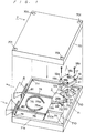
- the high-frequency integrated circuit comprises devices with a nonradiative dielectric waveguide, namely, an oscillator 1, a circulator 2, etc., and a mount case 7 with a nonradiative dielectric waveguide in which these devices are mounted.
- the oscillator 1 comprises a couple of rectangular conductive plates 10 and 11, a dielectric strip 12 and semiconductor chips (not shown) which are disposed between the conductive plates 10 and 11, a power terminal 16 and a modulating terminal 17.
- the conductive plates 10 and 11 are made of a conductive material such as aluminum, copper and the like.
- the conductive plate 11 has spacers 11b for keeping the space from the conductive plate 10 at a specified height a.
- the dielectric strip 12, as an example, is made of a dielectric material with a dielectric constant ( ⁇ r) of 2 such as fluororesin, and is designed to have a height a of 2.25mm and a width b of 2.5mm.
- the conductive plates 10 and 11 have tapped holes 18a at the respective four corners. By tightening screws 18b into the tapped holes 18a, the dielectric strip 12 and the semiconductor chips are fixed between the conductive plates 10 and 11.
- the conductive plate 11 has a plane mounting surface 19a on the lower side.
- the laminated conductive plates 10 and 11 have an end surface 19b on which an end 12a of the dielectric strip 12 shows, and the end surface 19b is vertical to a direction in which a high-frequency electromagnetic wave travels.
- the oscillator 1 outputs an electromagnetic wave to the circulator 2 through the end 12a of the dielectric strip 12.
- the circulator 2 comprises a couple of triangular conductive plates 20 and 21, and three dielectric strips 22 (although only one dielectric strip is seen in Fig. 1) and magnetic parts (not shown) which are disposed between the conductive plates 20 and 21.
- the conductive plates are made of a conductive material such as aluminum, copper and the like. Between the conductive plates 20 and 21, spacers 26 for keeping the space therebetween at the height a are provided at the three corners. Tapped holes (not shown) are made in the conductive plates 20 and 21 at the respective three corners such that the tapped holes communicate with the spacers 26. By tightening screws 27 into the tapped holes, the dielectric strips 22 and the magnetic parts are fixed between the conductive plates 20 and 21.
- the conductive plate 20 has a plane mounting surface 29a on the lower side (see Fig. 12).
- a plane mounting surface 29a on the lower side (see Fig. 12).
- respective ends 22a of the dielectric strips 22 show (see Fig. 12), and the end surfaces 29b are vertical to directions in which a high-frequency electromagnetic wave which is inputted or outputted through the ends 22a of the dielectric strips 22 travels.
- the mount case 7 comprises a rectangular upper conductive plate 70, a rectangular lower conductive plate 71, and dielectric strips 72, 73, 74, 75 and 76 disposed between the conductive plates 70 and 71.
- the dielectric strips 72, 73, 74, 75 and 76, and nonreflective terminals 75a are glued to the lower conductive plate 71.
- the lower conductive plate 71 has spacers 71a on the four peripheral sides so as to make a specified space from the upper conductive plate 70. Tapped holes 701 and 711 are made in the conductive plates 70 and 71 at the respective four corners such that the conductive plates 70 and 71 can be fixed to each other.
- the dielectric strip 73 serves as a nonreflective terminal.
- the nonreflective terminals 75a are provided at both ends of the dielectric strip 75.
- the lower conductive plate 71 has recesses 710 which are of the respective configurations of the oscillator 1, the circulator 2 and a mixer (not shown).
- the upper conductive plate 70 has recesses (not shown) of the same configurations.
- the conductive plates 70 and 71 are plates of a conductive material or plates of an insulating material with a metallised surface. Tapped holes 710a are made in each of the recesses 710, and the oscillator 1, the circulator 2 and the mixer are fixed in the respective recesses 710 by the screws 18b and 27. Also, it is possible to nip the oscillator 1, the circulator 2 and the mixer between the conductive plates 70 and 71 or to fix these devices in the recesses 710 by solder or conductive paste.
- One end of the dielectric strip 72 is in contact with the end 12a of the dielectric strip 12 of the oscillator 1, and the other end of the dielectric strip 72 is in contact with the end 22a of one of the dielectric strips 22 of the circulator 2.
- One end of the dielectric strip 73 is in contact with the end 22a of another of the dielectric strips 22 of the circulator 2.
- One end of the dielectric strip 74 is in contact with the end 22a of the other dielectric strip 22 of the circulator 2, and the other end of the dielectric strip 74 is in contact with an end of a transmitting rod 81 of the antenna 8.
- One end of the dielectric strip 76 is in contact with an end of a dielectric strip of the mixer, and the other end of the dielectric strip 76 is in contact with an end of a receiving rod 82 of the antenna 8.
- the conductive plates 70 and 71, the dielectric strips 74, 75 and 76, and the nonreflective terminals 75a form a coupler.
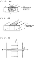
- Figs. 2A, 2B and 2C show a jig 6 for measuring the characteristics of the oscillator 1.
- the jig 6 comprises a mount section 60 and a converting section 61.
- the mount section 60 is formed in a part of a base plate 601 which is made of a conductive material such as aluminum, copper and the like.
- the base plate 601 has a couple of side walls 601a for positioning the oscillator 1.
- the base plate 601 further has tapped holes 601b, and when the oscillator 1 is mounted in the mount section 60 with the mounting surface 19a on the base plate 601, the tapped holes 18a of the oscillator 1 communicate with the tapped holes 601b of the base plate 601. Therefore, the oscillator 1 can be fixed on the base plate 601 by the screws 18b.
- the converting section 61 is to connect the oscillator 1 to a transmission line, for example, a metal tubular waveguide.
- the converting section 61 comprises a pressing section 610, a dielectric strip 62, a horn 611 and a metal tubular waveguide 612.
- the dielectric strip 62 is partly fixed between the base plate 601 and a pressing plate 610a by screws 610b.
- the horn 611 is fixed to the pressing section 610 by joining a flange 611a thereof to the pressing section 610 by a screw 611b.
- the waveguide 612 has a flange 612a on its end.
- an end surface 61a on which an end 62a of the dielectric strip 62 shows is formed, and the end surface 61a is vertical to a direction in which an electromagnetic wave is propagated in the dielectric strip 62.
- the other end 62b of the dielectric strip 62 is tapered in the width way such that the characteristic impedance of the dielectric strip 62 will match the characteristic impedance of the transmission line to which the metal tubular waveguide 612 is connected.
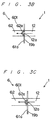
- Fig. 3A is a plan view of a connecting portion between the dielectric strip 12 of the oscillator 1 and the dielectric strip 62 of the measuring jig 6, that is, the exposed end 12a of the dielectric strip 12 and the exposed end 62a of the dielectric strip 62.
- the ends 12a and 62a of the dielectric strips 12 and 62 are vertical to a direction in which an electromagnetic wave is propagated and are on a level with the end surface 19b of the oscillator 1 and the end surface 61a of the pressing section 610, respectively.
- the ends 12a and 62a are in contact with each other.
- the connection between the dielectric strips 12 and 62 is possible in other ways as illustrated in Figs. 3B and 3C.
- the ends 12a and 62a of the dielectric strips 12 and 62 are wedges which engage with each other.
- the end 12a is slightly protruded from the end surface 19b of the oscillator 1.
- the ends 12a and 62a of the dielectric strips 12 and 62 are round which engage with each other, and the end 12a is slightly protruded from the end surface 19b of the oscillator 1.
- the ends 12a and 62a of the dielectric strips 12 and 62 do not have to be vertical to the electromagnetic wave propagation direction as long as the ends 12a and 62a engage with each other. It is also possible that the ends 12a and 62a which are vertical to the electromagnetic wave propagation direction are slightly protruded from the respective end surfaces 19b and 61a and are put into contact with each other.
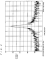
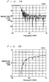
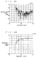
- Fig. 4 is a graph showing the oscillation characteristic of the oscillator 1. As is apparent from the graph of Fig. 4, an oscillation signal which has a resonance frequency of about 60GHz and has a good waveform was outputted from the end 12a of the dielectric strip 12.
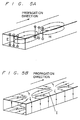
- Figs. 5A and 5B show an electromagnetic wave propagated in a metal tubular waveguide in TE10 mode.
- Fig. 5A shows the electric field E and the magnetic field H of the electromagnetic wave
- Fig. 5B shows the surface current I.
- Figs. 6A, 6B and 6C show an electromagnetic wave propagated in a nonradiative dielectric waveguide in LSM01 mode.
- Fig. 6A shows the electric field E and the magnetic field H of the electromagnetic wave
- Figs. 6B and 6C show the surface current 1.
- Fig. 6C shows a state wherein the nonradiative dielectric waveguide is cut off at a line B-B'.
- the surface current I of an electromagnetic wave propagated in a metal tubular waveguide has a component in the electromagnetic wave propagation direction. Therefore, in connecting the metal tubular waveguide to another metal tubular waveguide, the waveguides must be joined firmly without space by a flange. Otherwise, the surface current I will not flow from one of the waveguides to the other waveguide.
- the surface current I of an electromagnetic wave propagated in a nonradiative dielectric waveguide in LSM01 mode has only a component in a direction perpendicular to the electromagnetic wave propagation direction. Therefore, even if the conductive plates and the dielectric strip of the nonradiative dielectric waveguide are cut off perpendicularly to the electromagnetic wave propagation direction, that is, even if the nonradiative dielectric waveguide has a gap, the gap will not influence transmission of the electromagnetic wave.
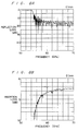
- Figs. 7A and 7B show the characteristics when the gap d was 0.
- Figs. 8A and 8B show the characteristics when the gap d was 0.1mm.
- the reflection loss and the insertion loss of the oscillator 1 were only a little increased when the oscillator 1 had a gap of 0.1mm.
- the inventors conducted an experiment in the following way.
- the conductive plates 10 and 11 and the dielectric strip 12 were cut off perpendicularly to the electromagnetic wave propagation direction. Then, the cut ends of the dielectric strip 12 were put into contact again, while the conductive plates 10 and 11 were rearranged to have a gap d between the respective cut ends. In this state, the characteristics of the oscillator 1 were measured.
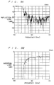
- Figs. 9A and 9B show the characteristics when the gap d was 0, and more specifically when the cut ends of the dielectric strip 12 and the cut ends of the conductive plates 10 and 11 were joined again.
- Figs. 10A and 10B show the characteristics when the gap d was 0.1mm, and more specifically when the cut ends of the dielectric strip 12 were protruded from the respective cut ends of the conductive plates 10 and 11 by 0.05mm and were put into contact with each other.
- Figs. 11A and 11B show the characteristics when the gap d was 0.2mm, and more specifically when the cut ends of the dielectric strip 12 were protruded from the respective cut ends of the conductive plates 10 and 11 by 0.1mm and were put into contact with each other.
- Fig. 12 shows the general structure of a measuring jig 6C for measuring the characteristics of the circulator 2.
- the same parts and members which are used for the measuring jig 6 are provided with the same reference symbols, and the description of these parts and members is omitted.
- the measuring jig 6C Since the circulator 2 has three exposed ends 22a of the dielectric strips 22, that is, three ports, the measuring jig 6C has a structure which is a combination of three measuring jigs 6.
- the circulator 2 is placed in a mount section 60 of the measuring jig 6C guided by three vertical surfaces 61a. In this moment, if even one of the screws 27 comes off the circulator 2, the dielectric strips 22 may be out of position. In order to prevent this trouble, a lid 67 is put on the circulator 2, and the circulator 2 is fixed in the measuring jig 6C by screws 68. In this state, the characteristics of the circulator 2 are measured.
- the electromagnetic wave When a high-frequency electromagnetic wave is inputted into the circulator 2 through one of the three ports (one of the ends 22a of the strips 22), the electromagnetic wave is propagated only to a specified one of the other two ports.
- the inventors evaluated the circulator 2 by using the measuring jig 6C and a network analyzer. The evaluation was carried out while the circulator 2 is used as an isolator with one of the ends 22a of the dielectric strips 22 serving as a nonreflective terminal.
- Figs. 13A and 13B show the results of the evaluation. As is apparent from Figs. 13A and 13B, the circulator 2 has a good isolation characteristic, a good insertion loss characteristic and a good reflection loss characteristic.
- the characteristics of the circulator 2 can be measured only by setting and screwing the circulator 2 in the measuring jig 6C.
- the connection between the circulator 2 and the measuring jig 6C does not require firm joining by use of a flange, and pushing between the ends 22a of the dielectric strips 22 and the ends 62a of the dielectric strips 62 is not necessary.
- the circulator 2 is fixed in the measuring jig 6C with the mounting surface 29a of the circulator 2 on the mount section 60, an electromagnetic wave is propagated to a specified one of the dielectric strips 62 through the dielectric strips 22 in LSM01 mode without mismatching and with a small loss.
- the characteristics of the circulator 2 can be measured accurately in a simple way.
- a measuring jig for a four-port device with a nonradiative dielectric waveguide should be structured as a combination of four measuring jigs 6.
- the measuring jig 6 can be used for evaluation of other one-port devices with a nonradiative dielectric waveguide as well as the oscillator 1. If the results of the evaluation of the oscillator 1, the circulator 2 and the mixer are good, these devices are surface-mounted in the respective recesses 710 of the conductive plate 71 of the mount case 7.
- the oscillator 1, the circulator 2 and the mixer are surface-mounted close to or in contact with the dielectric strips 72, 73, 74 and 76. Accordingly, there is no fear that the surface mounting will change the characteristics of the oscillator 1, the circulator 2 and the mixer, and these devices can perform the characteristics as measured in the evaluation by use of the measuring jigs 6 and 6C. Consequently, the produced integrated circuit is good in productivity and reliability.
- the oscillator 1, the circulator 2 and the mixer are screwed to the conductive plate 71, it is possible to use solder or conductive paste to fix the devices on the conductive plate 71.
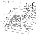
- Fig. 14 is a perspective view of a high-frequency integrated circuit which is another embodiment of the present invention.
- the same parts and members which are used for the embodiment of Fig. 1 are provided with the same reference symbols, and the description thereof is omitted.
- the distinctive point of this embodiment is that the upper conductive plate 70 has three windows 702 through which the oscillator 1, the circulator 2 and the mixer are mounted in the mount case 7. These windows 702 are positioned right above the recesses 710 of the lower conductive plate 71.
- the upper conductive plate 70 is screwed down to the lower conductive plate 71.
- the dielectric strips 72, 73, 74, 75 and 76, and the nonreflective terminals 75a can be fixed between the conductive plates 70 and 71.
- the mass productivity of the mount case 7 is improved.
- the dielectric strips of these devices can be put into contact with the dielectric strips in the mount case 7 accurately.
- the integrated circuit can be produced easily and is suited for mass production.
- the oscillator 1, the circulator 2 and/or the mixer can be exchanged without separating the conductive plates 70 and 71, and this is convenient for maintenance.
- the devices with a nonradiative dielectric waveguide are an oscillator, a circulator and a mixer.
- the present invention is applicable to a high-frequency integrated circuit which employs other devices with a nonradiative dielectric waveguide.
- the embodiments are integrated circuits which operate in a millimeter wave band, the present invention is applicable to integrated circuits which operate in a microwave band.
Landscapes
- Engineering & Computer Science (AREA)
- Radar, Positioning & Navigation (AREA)
- Remote Sensing (AREA)
- Computer Networks & Wireless Communication (AREA)
- Physics & Mathematics (AREA)
- General Physics & Mathematics (AREA)
- Waveguides (AREA)
- Inductance-Capacitance Distribution Constants And Capacitance-Resistance Oscillators (AREA)
- Radar Systems Or Details Thereof (AREA)
- Waveguide Connection Structure (AREA)
Abstract
Description
- The present invention relates to a high-frequency integrated circuit, and more particularly to a high-frequency integrated circuit which has a nonradiative dielectric waveguide and operates in a microwave band or in a millimeter wave band.
- It is well known that dielectric strips are arranged between a couple of conductive plates which are parallel to each other at a specified space to form a nonradiative dielectric waveguide which propagates an electromagnetic wave in LSM01 mode or LSE01 mode. For example, if the dielectric strips are designed to be made of a dielectric material with a dielectric constant (ε r) of 2 such as fluororesin and to have a width b of 2.5mm and a height a of 2.25mm, the dielectric strips will form a nonradiative dielectric waveguide which propagates an electromagnetic wave in a band of 60GHz. When these dielectric strips are put between two conductive plates, an electromagnetic wave which has a wavelength more than twice the height a hardly leaks from the dielectric strips. Therefore, an electromagnetic wave in LSM01 mode or in LSE01 mode is propagated along the dielectric strips without radiating, that is, with a small loss. Thus, such a nonradiative dielectric waveguide is suited to be used as a transmission line of a microwave or a millimeter wave.
- Since it is possible to provide magnetic parts and semiconductor chips as well as dielectric strips between a couple of conductive plates, a circulator, an oscillator and the like which have a nonradiative dielectric waveguide can be formed. In this way, a high-frequency integrated circuit which operates in a microwave band or in a millimeter wave band can be produced.
- In producing such a high-frequency integrated circuit, first, evaluation is conventionally carried out. For example, in producing an FM-CW radar, dielectric strips, magnetic parts and semiconductor chips are arranged between a couple of conductive plates for evaluation to form a circulator, an oscillator and so on. The conductive plates are connected to an evaluation terminal, and the characteristics of the whole circuit which is composed of the circulator, the oscillator, etc. are measured. Then, the dielectric strips, the magnetic parts and the semiconductor chips are dismounted from the conductive plates for evaluation, and these parts are rearranged between another couple of conductive plates to produce an integrated circuit.
- However, in this method, it is difficult to rearrange the circulator, the oscillator, etc. in the same way to reproduce an integrated circuit with the characteristics as measured. In this method, it is impossible to evaluate and adjust the circulator, the oscillator, etc. individually. Therefore, the mass productivity of the integrated circuit is not good. Further, when the integrated circuit has a trouble, and a part of the integrated circuit, for example, the circulator or the oscillator is exchanged, the change of the part may influence the whole circuit.
- An object of the present invention is to provide a high-frequency integrated circuit and components thereof which are suited for mass production.
- In order to attain the object, a high-frequency integrated circuit according to the present invention has a device with a nonradiative dielectric waveguide and a mount case with a nonradiative dielectric waveguide. The device with a nonradiative dielectric waveguide comprises: a couple of first conductors which are parallel to each other at a specified space; a first dielectric strip which is disposed between the first conductors; a plane mounting surface which is formed on one of the first conductors; and an end surface which is formed on an end of the first conductors so as to be vertical to a direction in which an electromagnetic wave is propagated in the first dielectric strip, an end of the first dielectric strip being exposed on the end surface. The mount case with a nonradiative dielectric waveguide comprises: a couple of second conductors which are parallel to each other at a specified space, the device with a nonradiative dielectric waveguide being placed between the second conductors; and a second dielectric strip which is disposed between the second conductors.
- The device with a nonradiative dielectric waveguide and the mount case with a nonradiative dielectric waveguide are produced separately. The device is evaluated, and thereafter, the device is mounted in the mount case. If necessary, the device can be dismounted from the mount case easily.
- This and other objects and features of the present invention will be apparent from the following description with reference to the accompanying drawings, in which:
- Fig. 1 is an exploded perspective view of a high-frequency integrated circuit which is an embodiment of the present invention;
- Fig. 2A is a perspective view of a measuring jig for evaluating an oscillator of the integrated circuit;
- Fig. 2B is a perspective view of the measuring jig and the oscillator mounted therein;
- Fig. 2C is a sectional view of the measuring jig and the oscillator, taken along a line
 C-C in Fig. 2B;
 - Fig. 3A is an internal plan view of a connecting portion between a dielectric strip of the oscillator and a dielectric strip of the measuring jig;
- Fig. 3B is an internal plan view of a modification of the connecting portion between the dielectric strip of the oscillator and the dielectric strip of the measuring jig;
- Fig. 3C is an internal plan view of another modification of the connecting portion between the dielectric strip of the oscillator and the dielectric strip of the measuring jig;
- Fig. 4 is a graph which shows an oscillation characteristic of the oscillator;
- Fig. 5A is a distribution chart which shows an electric field and a magnetic field of an electromagnetic wave which is propagated in a metal tubular waveguide in TE10 mode;
- Fig. 5B is a distribution chart which shows a surface current of the electromagnetic wave which is propagated in the metal tubular waveguide in TE10 mode;
- Fig. 6A is a distribution chart which shows an electric field and a magnetic field of an electromagnetic wave which is propagated in a nonradiative dielectric waveguide in LSM01 mode;
- Fig. 6B is a distribution chart which shows a surface current of the electromagnetic wave which is propagated in the nonradiative dielectric waveguide in LSM01 mode;
- Fig. 6C is a plane distribution chart which shows the surface current of the electromagnetic wave when the nonradiative dielectric waveguide is cut off at a line B-B';
- Fig. 7A is a graph which shows a reflection loss characteristic of the oscillator when the conductive plates and the dielectric strip have a gap of 0;
- Fig. 7B is a graph which shows an insertion loss characteristic of the oscillator when the conductive plates and the dielectric strip have a gap of 0;
- Fig. 8A is a graph which shows a reflection loss characteristic of the oscillator when the conductive plates and the dielectric strip have a gap of 0.1mm;
- Fig. 8B is a graph which shows an insertion loss characteristic of the oscillator when the conductive plates and the dielectric strip have a gap of 0.1mm;
- Fig. 9A is a graph which shows a reflection loss characteristic of the oscillator when the conductive plates and the dielectric strip have a gap of 0;
- Fig. 9B is a graph which shows an insertion loss characteristic of the oscillator when the conductive plates and the dielectric strip have a gap of 0;
- Fig. 10A is a graph which shows a reflection loss characteristic of the oscillator when only the conductive plates have a gap of 0.1mm;
- Fig. 10B is a graph which shows an insertion loss characteristic of the oscillator when only the conductive plates have a gap of 0.1mm;
- Fig. 11A is a graph which shows a reflection loss characteristic of the oscillator when only the conductive plates have a gap of 0.2mm;
- Fig. 11B is a graph which shows an insertion loss characteristic of the oscillator when only the conductive plates have a gap of 0.2mm;
- Fig. 12 is a perspective view of a measuring jig for evaluating a circulator of the integrated circuit of Fig. 1;
- Fig. 13A is a graph which shows an insertion loss characteristic and an isolation characteristic of the circulator;
- Fig. 13B is a graph which shows a reflection loss characteristic of the circulator; and
- Fig. 14 is a partial perspective view of a high-frequency integrated circuit which is another embodiment of the present invention.
- A high-frequency integrated circuit which is an embodiment of the present invention is described with reference to the accompanying drawings.
- The high-frequency integrated circuit is used, for example, as a high frequency section of an FM-CW radar which operates in a millimeter wave band. Further, by providing an antenna 8 to the high frequency section, the high frequency section is used as a radar head. The high-frequency integrated circuit comprises devices with a nonradiative dielectric waveguide, namely, an
oscillator 1, acirculator 2, etc., and amount case 7 with a nonradiative dielectric waveguide in which these devices are mounted. - As shown in Fig. 1, the
oscillator 1 comprises a couple of rectangularconductive plates dielectric strip 12 and semiconductor chips (not shown) which are disposed between theconductive plates power terminal 16 and a modulatingterminal 17. Theconductive plates conductive plate 11 hasspacers 11b for keeping the space from theconductive plate 10 at a specified height a. Thedielectric strip 12, as an example, is made of a dielectric material with a dielectric constant (ε r) of 2 such as fluororesin, and is designed to have a height a of 2.25mm and a width b of 2.5mm. Theconductive plates holes 18a at the respective four corners. By tighteningscrews 18b into the tappedholes 18a, thedielectric strip 12 and the semiconductor chips are fixed between theconductive plates - The
conductive plate 11 has aplane mounting surface 19a on the lower side. The laminatedconductive plates end surface 19b on which anend 12a of thedielectric strip 12 shows, and theend surface 19b is vertical to a direction in which a high-frequency electromagnetic wave travels. Theoscillator 1 outputs an electromagnetic wave to thecirculator 2 through theend 12a of thedielectric strip 12. - The
circulator 2 comprises a couple of triangularconductive plates conductive plates conductive plates spacers 26 for keeping the space therebetween at the height a are provided at the three corners. Tapped holes (not shown) are made in theconductive plates spacers 26. By tighteningscrews 27 into the tapped holes, thedielectric strips 22 and the magnetic parts are fixed between theconductive plates - The
conductive plate 20 has a plane mounting surface 29a on the lower side (see Fig. 12). On the threeend surfaces 29b of the laminatedconductive plates dielectric strips 22 show (see Fig. 12), and the end surfaces 29b are vertical to directions in which a high-frequency electromagnetic wave which is inputted or outputted through theends 22a of thedielectric strips 22 travels. - The
mount case 7 comprises a rectangular upperconductive plate 70, a rectangular lowerconductive plate 71, anddielectric strips conductive plates nonreflective terminals 75a are glued to the lowerconductive plate 71. The lowerconductive plate 71 hasspacers 71a on the four peripheral sides so as to make a specified space from the upperconductive plate 70. Tappedholes conductive plates conductive plates dielectric strip 73 serves as a nonreflective terminal. Thenonreflective terminals 75a are provided at both ends of thedielectric strip 75. The lowerconductive plate 71 hasrecesses 710 which are of the respective configurations of theoscillator 1, thecirculator 2 and a mixer (not shown). Likewise, the upperconductive plate 70 has recesses (not shown) of the same configurations. - The
conductive plates holes 710a are made in each of therecesses 710, and theoscillator 1, thecirculator 2 and the mixer are fixed in therespective recesses 710 by thescrews oscillator 1, thecirculator 2 and the mixer between theconductive plates recesses 710 by solder or conductive paste. - One end of the dielectric strip 72 is in contact with the
end 12a of thedielectric strip 12 of theoscillator 1, and the other end of the dielectric strip 72 is in contact with theend 22a of one of thedielectric strips 22 of thecirculator 2. One end of thedielectric strip 73 is in contact with theend 22a of another of thedielectric strips 22 of thecirculator 2. One end of thedielectric strip 74 is in contact with theend 22a of the otherdielectric strip 22 of thecirculator 2, and the other end of thedielectric strip 74 is in contact with an end of a transmittingrod 81 of the antenna 8. One end of thedielectric strip 76 is in contact with an end of a dielectric strip of the mixer, and the other end of thedielectric strip 76 is in contact with an end of a receivingrod 82 of the antenna 8. - The
conductive plates nonreflective terminals 75a form a coupler. - Figs. 2A, 2B and 2C show a
jig 6 for measuring the characteristics of theoscillator 1. Thejig 6 comprises amount section 60 and a convertingsection 61. Themount section 60 is formed in a part of abase plate 601 which is made of a conductive material such as aluminum, copper and the like. Thebase plate 601 has a couple ofside walls 601a for positioning theoscillator 1. Thebase plate 601 further has tappedholes 601b, and when theoscillator 1 is mounted in themount section 60 with the mountingsurface 19a on thebase plate 601, the tappedholes 18a of theoscillator 1 communicate with the tappedholes 601b of thebase plate 601. Therefore, theoscillator 1 can be fixed on thebase plate 601 by thescrews 18b. - The converting
section 61 is to connect theoscillator 1 to a transmission line, for example, a metal tubular waveguide. The convertingsection 61 comprises apressing section 610, adielectric strip 62, ahorn 611 and ametal tubular waveguide 612. In thepressing section 610, thedielectric strip 62 is partly fixed between thebase plate 601 and apressing plate 610a byscrews 610b. Thehorn 611 is fixed to thepressing section 610 by joining aflange 611a thereof to thepressing section 610 by ascrew 611b. Thewaveguide 612 has aflange 612a on its end. - On the side of the converting
section 61 which faces theoscillator 1, anend surface 61a on which anend 62a of thedielectric strip 62 shows is formed, and theend surface 61a is vertical to a direction in which an electromagnetic wave is propagated in thedielectric strip 62. Theother end 62b of thedielectric strip 62 is tapered in the width way such that the characteristic impedance of thedielectric strip 62 will match the characteristic impedance of the transmission line to which themetal tubular waveguide 612 is connected. - Fig. 3A is a plan view of a connecting portion between the
dielectric strip 12 of theoscillator 1 and thedielectric strip 62 of the measuringjig 6, that is, theexposed end 12a of thedielectric strip 12 and theexposed end 62a of thedielectric strip 62. The ends 12a and 62a of thedielectric strips end surface 19b of theoscillator 1 and theend surface 61a of thepressing section 610, respectively. The ends 12a and 62a are in contact with each other. The connection between thedielectric strips - In Fig. 3B, the
ends dielectric strips end 12a is slightly protruded from theend surface 19b of theoscillator 1. In Fig. 3C, theends dielectric strips end 12a is slightly protruded from theend surface 19b of theoscillator 1. As in the cases of Figs. 3B and 3C, theends dielectric strips ends ends - Next, the action of the
oscillator 1 is described. When a direct current is supplied to thepower terminal 16 of theoscillator 1, a high-frequency electromagnetic wave is generated and inputted into thedielectric strip 12. Suppose that the space between theconductive plates 
conductive plates dielectric strip 12. The electromagnetic wave is propagated in thedielectric strip 12 and is outputted through theend 12a. When theoscillator 1 is mounted in the measuringjig 6, theoscillator 1 acts in the same way, and the electromagnetic wave is outputted through theend 12a in thepressing section 610. Possible transmission modes of an electromagnetic wave in a nonradiative dielectric waveguide are generally LSE mode and LSM mode. In order for a small loss, LSM01 mode which is the lowest mode of LSM mode is usually used. - The inventors evaluated the
oscillator 1 by using the measuringjig 6 and a spectrum analyser. Fig. 4 is a graph showing the oscillation characteristic of theoscillator 1. As is apparent from the graph of Fig. 4, an oscillation signal which has a resonance frequency of about 60GHz and has a good waveform was outputted from theend 12a of thedielectric strip 12. - Now, the difference between an electromagnetic wave propagated in a metal tubular waveguide and an electromagnetic wave propagated in a nonradiative dielectric waveguide is described. Figs. 5A and 5B show an electromagnetic wave propagated in a metal tubular waveguide in TE10 mode. Fig. 5A shows the electric field E and the magnetic field H of the electromagnetic wave, and Fig. 5B shows the surface current I. Figs. 6A, 6B and 6C show an electromagnetic wave propagated in a nonradiative dielectric waveguide in LSM01 mode. Fig. 6A shows the electric field E and the magnetic field H of the electromagnetic wave, and Figs. 6B and 6C show the surface current 1. Fig. 6C shows a state wherein the nonradiative dielectric waveguide is cut off at a line B-B'.
- As is apparent from Fig. 5B, the surface current I of an electromagnetic wave propagated in a metal tubular waveguide has a component in the electromagnetic wave propagation direction. Therefore, in connecting the metal tubular waveguide to another metal tubular waveguide, the waveguides must be joined firmly without space by a flange. Otherwise, the surface current I will not flow from one of the waveguides to the other waveguide.
- On the other hand, the surface current I of an electromagnetic wave propagated in a nonradiative dielectric waveguide in LSM01 mode, as is apparent from Fig. 6B, has only a component in a direction perpendicular to the electromagnetic wave propagation direction. Therefore, even if the conductive plates and the dielectric strip of the nonradiative dielectric waveguide are cut off perpendicularly to the electromagnetic wave propagation direction, that is, even if the nonradiative dielectric waveguide has a gap, the gap will not influence transmission of the electromagnetic wave.
- In order to prove this assumption, the inventors measured the characteristics of the
oscillator 1 when theconductive plates dielectric strip 12 were cut off to have a gap d in a direction perpendicular to the electromagnetic wave propagation direction. Figs. 7A and 7B show the characteristics when the gap d was 0. Figs. 8A and 8B show the characteristics when the gap d was 0.1mm. As is apparent from Figs. 7A through 8B, the reflection loss and the insertion loss of theoscillator 1 were only a little increased when theoscillator 1 had a gap of 0.1mm. - Now, this is applied to the connection between the
dielectric strip 12 of theoscillator 1 and thedielectric strip 62 of the measuringjig 6. The case of Figs. 7A and 7B corresponds to a case wherein theend surface 19b of theoscillator 1 and theend 12a of thedielectric strip 12 are in contact with theend surface 61a of thepressing section 610 and theend 62a of thestrip 62, respectively (d = 0 in Fig. 3A). The case of Figs. 8A and 8B corresponds to a case wherein there is a gap d of 0.1mm between the level of theend surface 19b and theend 12a and the level of theend surface 61a and theend 62a (d = 0.1mm in Fig. 3A). From the result of the experiment, it can be inferred that a slight gap between theend 12a and theend 62a is allowable. Accordingly, the connection between theoscillator 1 and the measuringjig 6 does not require firm joining by use of a flange, and pushing between theend 12a of thedielectric strip 12 and theend 62a of thedielectric strip 62 is not necessary. Therefore, only by mounting theoscillator 1 in themount section 60 of the measuringjig 6 with the mountingsurface 19b of theoscillator 1 on thebase plate 601, an electromagnetic wave is propagated in thedielectric strips oscillator 1 can be measured accurately in a simple way. - Further, in order to estimate the characteristics in a case wherein the
end 12a of thedielectric strip 12 and theend 62a of thedielectric strip 62 which are slightly protruded from the end surfaces 19b and 61a respectively are put into contact with each other, the inventors conducted an experiment in the following way. Theconductive plates dielectric strip 12 were cut off perpendicularly to the electromagnetic wave propagation direction. Then, the cut ends of thedielectric strip 12 were put into contact again, while theconductive plates oscillator 1 were measured. - Figs. 9A and 9B show the characteristics when the gap d was 0, and more specifically when the cut ends of the
dielectric strip 12 and the cut ends of theconductive plates dielectric strip 12 were protruded from the respective cut ends of theconductive plates dielectric strip 12 were protruded from the respective cut ends of theconductive plates - As is apparent from Figs. 9A through 11B, even if there is a gap d between the
conductive plates oscillator 1 hardly change as long as the cut ends of thedielectric strip 12 are in contact with each other. This is applicable to the connection between theoscillator 1 and the measuringjig 6. Therefore, even if theend 12a of thestrip 12 and theend 62a of thestrip 62 are slightly protruded from the respective end surfaces 19b and 61a, as long as theends - Fig. 12 shows the general structure of a measuring
jig 6C for measuring the characteristics of thecirculator 2. In Fig. 12, the same parts and members which are used for the measuringjig 6 are provided with the same reference symbols, and the description of these parts and members is omitted. Since thecirculator 2 has three exposedends 22a of thedielectric strips 22, that is, three ports, the measuringjig 6C has a structure which is a combination of three measuringjigs 6. Thecirculator 2 is placed in amount section 60 of the measuringjig 6C guided by threevertical surfaces 61a. In this moment, if even one of thescrews 27 comes off thecirculator 2, thedielectric strips 22 may be out of position. In order to prevent this trouble, alid 67 is put on thecirculator 2, and thecirculator 2 is fixed in the measuringjig 6C by screws 68. In this state, the characteristics of thecirculator 2 are measured. - When a high-frequency electromagnetic wave is inputted into the
circulator 2 through one of the three ports (one of theends 22a of the strips 22), the electromagnetic wave is propagated only to a specified one of the other two ports. The inventors evaluated thecirculator 2 by using the measuringjig 6C and a network analyzer. The evaluation was carried out while thecirculator 2 is used as an isolator with one of theends 22a of thedielectric strips 22 serving as a nonreflective terminal. - Figs. 13A and 13B show the results of the evaluation. As is apparent from Figs. 13A and 13B, the
circulator 2 has a good isolation characteristic, a good insertion loss characteristic and a good reflection loss characteristic. - In this way, the characteristics of the
circulator 2 can be measured only by setting and screwing thecirculator 2 in the measuringjig 6C. The connection between thecirculator 2 and the measuringjig 6C does not require firm joining by use of a flange, and pushing between theends 22a of thedielectric strips 22 and theends 62a of thedielectric strips 62 is not necessary. When thecirculator 2 is fixed in the measuringjig 6C with the mounting surface 29a of thecirculator 2 on themount section 60, an electromagnetic wave is propagated to a specified one of thedielectric strips 62 through thedielectric strips 22 in LSM01 mode without mismatching and with a small loss. Thus, by using the measuringjig 6C, the characteristics of thecirculator 2 can be measured accurately in a simple way. - A measuring jig for a four-port device with a nonradiative dielectric waveguide should be structured as a combination of four measuring
jigs 6. The measuringjig 6 can be used for evaluation of other one-port devices with a nonradiative dielectric waveguide as well as theoscillator 1. If the results of the evaluation of theoscillator 1, thecirculator 2 and the mixer are good, these devices are surface-mounted in therespective recesses 710 of theconductive plate 71 of themount case 7. - As shown in Fig. 1, the
oscillator 1, thecirculator 2 and the mixer are surface-mounted close to or in contact with thedielectric strips oscillator 1, thecirculator 2 and the mixer, and these devices can perform the characteristics as measured in the evaluation by use of the measuringjigs - Although in Fig. 1, the
oscillator 1, thecirculator 2 and the mixer are screwed to theconductive plate 71, it is possible to use solder or conductive paste to fix the devices on theconductive plate 71. - Fig. 14 is a perspective view of a high-frequency integrated circuit which is another embodiment of the present invention. The same parts and members which are used for the embodiment of Fig. 1 are provided with the same reference symbols, and the description thereof is omitted. The distinctive point of this embodiment is that the upper
conductive plate 70 has threewindows 702 through which theoscillator 1, thecirculator 2 and the mixer are mounted in themount case 7. Thesewindows 702 are positioned right above therecesses 710 of the lowerconductive plate 71. - According to this embodiment, before mounting the
oscillator 1, thecirculator 2 and the mixer in themount case 7, the upperconductive plate 70 is screwed down to the lowerconductive plate 71. Thereby, the dielectric strips 72, 73, 74, 75 and 76, and thenonreflective terminals 75a can be fixed between theconductive plates nonreflective terminals 75a to the lowerconductive plate 71. Thereby, the mass productivity of themount case 7 is improved. After screwing the upperconductive plate 70 down to the lowerconductive plate 71, theoscillator 1, thecirculator 2 and the mixer are mounted in thecase 7 guided by therespective windows 702. Thereby, the dielectric strips of these devices can be put into contact with the dielectric strips in themount case 7 accurately. Thus, the integrated circuit can be produced easily and is suited for mass production. Additionally, theoscillator 1, thecirculator 2 and/or the mixer can be exchanged without separating theconductive plates - In the above embodiments, the devices with a nonradiative dielectric waveguide are an oscillator, a circulator and a mixer. However, the present invention is applicable to a high-frequency integrated circuit which employs other devices with a nonradiative dielectric waveguide. Although the embodiments are integrated circuits which operate in a millimeter wave band, the present invention is applicable to integrated circuits which operate in a microwave band.
- Although the present invention has been described in connection with the preferred embodiments above, it is to be noted that various changes and modifications are possible to those who are skilled in the art. Such changes and modifications are to be understood as being within the scope of the present invention.
Claims (9)
- A high-frequency integrated circuit comprising:
a device with a nonradiative dielectric waveguide comprising:
a couple of first conductors which are parallel to each other at a specified space;
a first dielectric strip which is disposed between the first conductors;
a plane mounting surface which is formed on one of the first conductors; and
an end surface which is formed on an end of the first conductors so as to be vertical to a direction in which an electromagnetic wave is propagated in the first dielectric strip, an end of the first dielectric strip being exposed on the end surface; and
a mount case with a nonradiative dielectric waveguide in which the device with a nonradiative dielectric waveguide is mounted, the mount case comprising:
a couple of second conductors which are parallel to each other at a specified space, the device with a nonradiative dielectric waveguide being placed between the second conductors; and
a second dielectric strip which is disposed between the second conductors. - A high-frequency integrated circuit as claimed in claim 1, wherein the exposed end of the first dielectric strip is close to an end of the second dielectric strip.
- A high-frequency integrated circuit as claimed in claim 1, wherein the exposed end of the first dielectric strip is in contact with an end of the second dielectric strip.
- A high-frequency integrated circuit as claimed in claim 1, wherein the exposed end of the dielectric strip has a projection which is protruded from the end surface of the first conductors.
- A high-frequency integrated circuit as claimed in claim 1, wherein the exposed end of the dielectric strip has a recess which is retracted from the end surface of the first conductors.
- A high-frequency integrated circuit as claimed in claim 1, wherein the device with a nonradiative dielectric waveguide is an oscillator.
- A high-frequency integrated circuit as claimed in claim 1, wherein the device with a nonradiative dielectric waveguide is a circulator.
- A high-frequency integrated circuit as claimed in claim 1, wherein one of the second conductors has a window through which the device with a nonradiative dielectric waveguide is mounted in the mount case.
- A high-frequency integrated circuit as claimed in claim 1, further comprising an antenna provided to the mount case.
Applications Claiming Priority (3)
| Application Number | Priority Date | Filing Date | Title |
|---|---|---|---|
| JP205427/94 | 1994-08-30 | ||
| JP20542794 | 1994-08-30 | ||
| JP20542794A JP3220967B2 (en) | 1994-08-30 | 1994-08-30 | Integrated circuit |
Publications (3)
| Publication Number | Publication Date |
|---|---|
| EP0700114A2 true EP0700114A2 (en) | 1996-03-06 |
| EP0700114A3 EP0700114A3 (en) | 1997-04-02 |
| EP0700114B1 EP0700114B1 (en) | 2001-03-21 |
Family
ID=16506680
Family Applications (1)
| Application Number | Title | Priority Date | Filing Date |
|---|---|---|---|
| EP95113571A Expired - Lifetime EP0700114B1 (en) | 1994-08-30 | 1995-08-29 | High-frequency integrated circuit |
Country Status (6)
| Country | Link |
|---|---|
| US (1) | US5604469A (en) |
| EP (1) | EP0700114B1 (en) |
| JP (1) | JP3220967B2 (en) |
| KR (1) | KR0175200B1 (en) |
| CN (1) | CN1054705C (en) |
| DE (1) | DE69520394T2 (en) |
Cited By (5)
| Publication number | Priority date | Publication date | Assignee | Title |
|---|---|---|---|---|
| EP0817394A2 (en) * | 1996-07-01 | 1998-01-07 | Murata Manufacturing Co., Ltd. | Transmitter-receiver |
| EP0838693A1 (en) * | 1996-10-23 | 1998-04-29 | Murata Manufacturing Co., Ltd. | Antenna-shared distributor and transmission and receiving apparatus using same |
| WO2001015262A1 (en) * | 1999-08-20 | 2001-03-01 | Sensing Tech. Corp. | Radio repeater using the non-radiative dielectric waveguide |
| CN102509833A (en) * | 2011-10-26 | 2012-06-20 | 电子科技大学 | Device for converting substrate integrated waveguide to coaxial waveguide |
| EP3695457A4 (en) * | 2017-10-11 | 2020-11-25 | Texas Instruments Incorporated | Interposer between microelectronic package substrate and dielectric waveguide connector |
Families Citing this family (13)
| Publication number | Priority date | Publication date | Assignee | Title |
|---|---|---|---|---|
| JP3220966B2 (en) * | 1994-08-30 | 2001-10-22 | 株式会社村田製作所 | Non-radiative dielectric line parts |
| JP3125974B2 (en) * | 1994-10-25 | 2001-01-22 | 本田技研工業株式会社 | NRD guide circuit, radar module and radar device |
| JPH08181510A (en) * | 1994-10-25 | 1996-07-12 | Honda Motor Co Ltd | Method for assembling nrd guide circuit and nrd guide circuit |
| JP3045046B2 (en) * | 1995-07-05 | 2000-05-22 | 株式会社村田製作所 | Non-radiative dielectric line device |
| US6094106A (en) * | 1997-06-25 | 2000-07-25 | Kyocera Corporation | Non-radiative dielectric waveguide module |
| KR100399532B1 (en) * | 1999-02-19 | 2003-09-26 | 양형칠 | Chemical Injection Method through the Space Grouting Rod |
| JP3570359B2 (en) * | 2000-08-24 | 2004-09-29 | 三菱電機株式会社 | High frequency module |
| JP4580815B2 (en) * | 2005-05-11 | 2010-11-17 | 株式会社東芝 | Microwave module |
| US7423497B2 (en) * | 2005-09-29 | 2008-09-09 | Indian Institute Of Technology | Device for coupling suspended stripline and NRD guides |
| US8614610B2 (en) * | 2010-09-07 | 2013-12-24 | Teledyne Scientific & Imaging, Llc | Ruggedized waveguide encapsulation fixture for receiving a compressed waveguide component |
| GB2518344B (en) * | 2013-07-02 | 2015-09-30 | Navtech Radar Ltd | Radar Head |
| US9935347B2 (en) * | 2015-11-23 | 2018-04-03 | L-3 Communications Corporation | Electronic circuit assembly having a carrier with holes therein for receiving and connecting waveguides having different dielectric constants |
| KR102546097B1 (en) * | 2021-08-25 | 2023-06-22 | (주)파트론 | Portable sound output device and control method thereof |
Citations (3)
| Publication number | Priority date | Publication date | Assignee | Title |
|---|---|---|---|---|
| US4091343A (en) * | 1975-06-30 | 1978-05-23 | Epsilon Lambda Electronics Corp. | Insular waveguide directional coupler |
| FR2528633A1 (en) * | 1982-06-09 | 1983-12-16 | Seki & Co Ltd | DIELECTRIC WAVEGUIDE |
| GB2185861A (en) * | 1985-01-16 | 1987-07-29 | Junkosha Co Ltd | Dielectric waveguide |
Family Cites Families (3)
| Publication number | Priority date | Publication date | Assignee | Title |
|---|---|---|---|---|
| US4677404A (en) * | 1984-12-19 | 1987-06-30 | Martin Marietta Corporation | Compound dielectric multi-conductor transmission line |
| EP0607044B1 (en) * | 1993-01-13 | 1999-08-11 | Honda Giken Kogyo Kabushiki Kaisha | Dielectric waveguide mixer and dielectric waveguide radar module |
| JP3123293B2 (en) * | 1993-03-05 | 2001-01-09 | 株式会社村田製作所 | Non-radiative dielectric line and method of manufacturing the same |
-
1994
- 1994-08-30 JP JP20542794A patent/JP3220967B2/en not_active Expired - Fee Related
-
1995
- 1995-08-28 US US08/519,949 patent/US5604469A/en not_active Expired - Lifetime
- 1995-08-29 KR KR1019950027302A patent/KR0175200B1/en not_active IP Right Cessation
- 1995-08-29 DE DE69520394T patent/DE69520394T2/en not_active Expired - Lifetime
- 1995-08-29 EP EP95113571A patent/EP0700114B1/en not_active Expired - Lifetime
- 1995-08-30 CN CN95116912A patent/CN1054705C/en not_active Expired - Fee Related
Patent Citations (3)
| Publication number | Priority date | Publication date | Assignee | Title |
|---|---|---|---|---|
| US4091343A (en) * | 1975-06-30 | 1978-05-23 | Epsilon Lambda Electronics Corp. | Insular waveguide directional coupler |
| FR2528633A1 (en) * | 1982-06-09 | 1983-12-16 | Seki & Co Ltd | DIELECTRIC WAVEGUIDE |
| GB2185861A (en) * | 1985-01-16 | 1987-07-29 | Junkosha Co Ltd | Dielectric waveguide |
Non-Patent Citations (2)
| Title |
|---|
| ELECTRONICS & COMMUNICATIONS IN JAPAN, PART II - ELECTRONICS, vol. 74, no. 2, 1 February 1991, pages 20-28, XP000240840 TSUKASA YONEYAMA: "MILLIMETER-WAVE INTEGRATED CIRCUITS USING NONRADIATIVE DIELECTRIC WAVEGUIDE" * |
| IEEE TRANSACTIONS ON MICROWAVE THEORY AND TECHNIQUES, vol. mtt-31, no. 12, December 1983, NEW YORK US, pages 1002-1008, XP002024534 TSUKASA YONEYAMA, SADAO FUJITA AND SHIGEO NISHIDA: "Insulated Nonradiative Dielectric Waveguide for Millimeter-Wave Integrated Circuits" * |
Cited By (10)
| Publication number | Priority date | Publication date | Assignee | Title |
|---|---|---|---|---|
| EP0817394A2 (en) * | 1996-07-01 | 1998-01-07 | Murata Manufacturing Co., Ltd. | Transmitter-receiver |
| EP0817394A3 (en) * | 1996-07-01 | 2001-02-07 | Murata Manufacturing Co., Ltd. | Transmitter-receiver |
| EP0838693A1 (en) * | 1996-10-23 | 1998-04-29 | Murata Manufacturing Co., Ltd. | Antenna-shared distributor and transmission and receiving apparatus using same |
| US6008755A (en) * | 1996-10-23 | 1999-12-28 | Murata Manufacturing Co., Ltd. | Antenna-shared distributor and transmission and receiving apparatus using same |
| WO2001015262A1 (en) * | 1999-08-20 | 2001-03-01 | Sensing Tech. Corp. | Radio repeater using the non-radiative dielectric waveguide |
| CN102509833A (en) * | 2011-10-26 | 2012-06-20 | 电子科技大学 | Device for converting substrate integrated waveguide to coaxial waveguide |
| CN102509833B (en) * | 2011-10-26 | 2013-09-25 | 电子科技大学 | Device for converting substrate integrated waveguide to coaxial waveguide |
| EP3695457A4 (en) * | 2017-10-11 | 2020-11-25 | Texas Instruments Incorporated | Interposer between microelectronic package substrate and dielectric waveguide connector |
| US10886590B2 (en) | 2017-10-11 | 2021-01-05 | Texas Instruments Incorporated | Interposer for connecting an antenna on an IC substrate to a dielectric waveguide through an interface waveguide located within an interposer block |
| US11799184B2 (en) | 2017-10-11 | 2023-10-24 | Texas Instruments Incorporated | Interposer between an integrated circuit antenna interface and an external waveguide interface including an internal waveguide coupled between these interfaces |
Also Published As
| Publication number | Publication date |
|---|---|
| DE69520394T2 (en) | 2002-01-03 |
| CN1054705C (en) | 2000-07-19 |
| KR960009268A (en) | 1996-03-22 |
| EP0700114A3 (en) | 1997-04-02 |
| EP0700114B1 (en) | 2001-03-21 |
| DE69520394D1 (en) | 2001-04-26 |
| CN1127434A (en) | 1996-07-24 |
| US5604469A (en) | 1997-02-18 |
| KR0175200B1 (en) | 1999-04-01 |
| JP3220967B2 (en) | 2001-10-22 |
| JPH0878913A (en) | 1996-03-22 |
Similar Documents
| Publication | Publication Date | Title |
|---|---|---|
| EP0700114B1 (en) | High-frequency integrated circuit | |
| EP0752734B1 (en) | Nonradiative dielectric wave guide apparatus and instrument for measuring characteristics of a circuit board | |
| US6218916B1 (en) | Electromagnetically coupling nonradiative dielectric waveguides | |
| US6580343B2 (en) | Dielectric waveguide with pairs of dielectric strips connected in an off-set manner | |
| US4810981A (en) | Assembly of microwave components | |
| US3757272A (en) | Strip transmission line coupler | |
| EP0700112B1 (en) | High-frequency integrated circuit | |
| EP0699915B1 (en) | Measuring jig used for evaluation of a device with a nonradiative dielectric waveguide | |
| US7253698B2 (en) | Line converter for coupling standing waves to a shield area of a three dimensional waveguide | |
| US5825268A (en) | Device with a nonradiative dielectric waveguide | |
| JP2003318614A (en) | Input/output structure of dielectric waveguide | |
| JPS59163573A (en) | High frequency power measuring device | |
| JP3723687B2 (en) | Connection structure between NRD guide and dielectric waveguide | |
| JPH06140815A (en) | Waveguide/trip line converter | |
| CA1195393A (en) | Aperture-coupled microwave apparatus | |
| JP3042063B2 (en) | Microwave circuit | |
| JPH11308002A (en) | Nonradioactive dielectric line, connector and jig for measurement | |
| JP3943759B2 (en) | Non-radioactive dielectric guide and manufacturing method thereof | |
| JP2000165113A (en) | High frequency circuit device and radio unit | |
| JPH03162104A (en) | Terminal connecting structure of microwave unit | |
| JPH11186818A (en) | Dielectric line connection device |
Legal Events
| Date | Code | Title | Description |
|---|---|---|---|
| PUAI | Public reference made under article 153(3) epc to a published international application that has entered the european phase |
Free format text: ORIGINAL CODE: 0009012 |
|
| AK | Designated contracting states |
Kind code of ref document: A2 Designated state(s): DE FR GB SE |
|
| PUAL | Search report despatched |
Free format text: ORIGINAL CODE: 0009013 |
|
| AK | Designated contracting states |
Kind code of ref document: A3 Designated state(s): DE FR GB SE |
|
| 17P | Request for examination filed |
Effective date: 19970425 |
|
| 17Q | First examination report despatched |
Effective date: 19981106 |
|
| GRAG | Despatch of communication of intention to grant |
Free format text: ORIGINAL CODE: EPIDOS AGRA |
|
| GRAG | Despatch of communication of intention to grant |
Free format text: ORIGINAL CODE: EPIDOS AGRA |
|
| GRAH | Despatch of communication of intention to grant a patent |
Free format text: ORIGINAL CODE: EPIDOS IGRA |
|
| GRAH | Despatch of communication of intention to grant a patent |
Free format text: ORIGINAL CODE: EPIDOS IGRA |
|
| GRAA | (expected) grant |
Free format text: ORIGINAL CODE: 0009210 |
|
| AK | Designated contracting states |
Kind code of ref document: B1 Designated state(s): DE FR GB SE |
|
| REF | Corresponds to: |
Ref document number: 69520394 Country of ref document: DE Date of ref document: 20010426 |
|
| ET | Fr: translation filed | ||
| REG | Reference to a national code |
Ref country code: GB Ref legal event code: IF02 |
|
| PLBE | No opposition filed within time limit |
Free format text: ORIGINAL CODE: 0009261 |
|
| STAA | Information on the status of an ep patent application or granted ep patent |
Free format text: STATUS: NO OPPOSITION FILED WITHIN TIME LIMIT |
|
| 26N | No opposition filed | ||
| PGFP | Annual fee paid to national office [announced via postgrant information from national office to epo] |
Ref country code: FR Payment date: 20090814 Year of fee payment: 15 |
|
| PGFP | Annual fee paid to national office [announced via postgrant information from national office to epo] |
Ref country code: SE Payment date: 20090806 Year of fee payment: 15 Ref country code: GB Payment date: 20090826 Year of fee payment: 15 Ref country code: DE Payment date: 20090827 Year of fee payment: 15 |
|
| EUG | Se: european patent has lapsed | ||
| GBPC | Gb: european patent ceased through non-payment of renewal fee |
Effective date: 20100829 |
|
| REG | Reference to a national code |
Ref country code: FR Ref legal event code: ST Effective date: 20110502 |
|
| REG | Reference to a national code |
Ref country code: DE Ref legal event code: R119 Ref document number: 69520394 Country of ref document: DE Effective date: 20110301 |
|
| PG25 | Lapsed in a contracting state [announced via postgrant information from national office to epo] |
Ref country code: DE Free format text: LAPSE BECAUSE OF NON-PAYMENT OF DUE FEES Effective date: 20110301 Ref country code: FR Free format text: LAPSE BECAUSE OF NON-PAYMENT OF DUE FEES Effective date: 20100831 |
|
| PG25 | Lapsed in a contracting state [announced via postgrant information from national office to epo] |
Ref country code: GB Free format text: LAPSE BECAUSE OF NON-PAYMENT OF DUE FEES Effective date: 20100829 |
|
| PG25 | Lapsed in a contracting state [announced via postgrant information from national office to epo] |
Ref country code: SE Free format text: LAPSE BECAUSE OF NON-PAYMENT OF DUE FEES Effective date: 20100830 |