EP0698911B1 - Position sensitive photomultiplier - Google Patents
Position sensitive photomultiplier Download PDFInfo
- Publication number
- EP0698911B1 EP0698911B1 EP95305888A EP95305888A EP0698911B1 EP 0698911 B1 EP0698911 B1 EP 0698911B1 EP 95305888 A EP95305888 A EP 95305888A EP 95305888 A EP95305888 A EP 95305888A EP 0698911 B1 EP0698911 B1 EP 0698911B1
- Authority
- EP
- European Patent Office
- Prior art keywords
- component
- anode
- end portion
- insulating
- fixed
- Prior art date
- Legal status (The legal status is an assumption and is not a legal conclusion. Google has not performed a legal analysis and makes no representation as to the accuracy of the status listed.)
- Expired - Lifetime
Links
Images


Classifications
-
- H—ELECTRICITY
- H01—ELECTRIC ELEMENTS
- H01J—ELECTRIC DISCHARGE TUBES OR DISCHARGE LAMPS
- H01J43/00—Secondary-emission tubes; Electron-multiplier tubes
- H01J43/04—Electron multipliers
- H01J43/06—Electrode arrangements
- H01J43/12—Anode arrangements
-
- H—ELECTRICITY
- H01—ELECTRIC ELEMENTS
- H01J—ELECTRIC DISCHARGE TUBES OR DISCHARGE LAMPS
- H01J43/00—Secondary-emission tubes; Electron-multiplier tubes
- H01J43/04—Electron multipliers
- H01J43/045—Position sensitive electron multipliers
Definitions
- the invention relates to an anode for a photomultiplier and to a photomultiplier comprising such an anode.
- the photomultiplier described in this prior art has a cross wire anode between a dynode unit constituted by mesh dynodes and a last-stage dynode. Photoelectrons emitted from a photoelectric surface are sequentially cascade-multiplied by the mesh dynode at each stage, thereby emitting secondary electrons. The secondary electrons pass through the cross wire anode and are further multiplied by the last-stage dynode.
- the secondary electrons multiplied by the last-stage dynode and orbit-inverted are captured by the cross wire anode and extracted outside the photomultiplier.
- the cross wire anode consists of two layers of anode groups in the X and Y directions perpendicular to each other.
- Each anode group is constituted by a plurality of wires arranged at a pitch of 3.0 to 7.0 mm and having a diameter of 0.5 to 1.0 mm.
- These wires are connected by resistor chains constituted by resistors connected in series. Secondary electrons extracted from wires of the upper and lower wire anode are shunted through the resistor chains and extracted from terminals X 1 and X 2 of one of the resistor chains and terminals Y 1 and Y 2 of another of the resistor chains.
- the terminals X 1 and X 2 are terminals of an X-component shunt circuit (resistor chain) constituted by resistors for electrically connecting between the wires of the upper wire anode.
- the terminals Y 1 and Y 2 are terminals of a Y-component shunt circuit (resistor chain) constituted by resistors for electrically connecting between the wires of the lower wire anode.
- the position (X, Y) means an incident position of a plane of incidence, where an incident weak light beam is reached.
- US-A-4,079,578 describes a charged particle detector array which comprises plural sets of electrode elements with each set comprising a plurality of linear extending parallel electrodes.
- EP-A-0 622 824 A1 relates to a photomultiplier which comprises a photocathode, an electron multiplier and an anode plate.
- the anode plate has electron through holes at a predetermined portion.
- Some of the embodiments of the invention relate to a photomultiplier for detecting an incident position of an incident plane in a X direction and Y direction, where a weak light beam is reached, and particularly has as its object to obtain a photomultiplier having a structure for minimizing crosstalk near the incident position of the weak light beam to improve the precision of position resolving power.
- an anode for a photomultiplier comprising a first component comprising a plurality of elongate planar conductors arranged substantially in parallel to a first axis, each planar conductor having a plurality of through holes formed along its length; a second component comprising a plurality of elongate planar conductors arranged substantially in parallel to a second axis, each planar conductor having a plurality of through holes formed along its length; and supporting means for supporting the first and second components with the first axis substantially orthogonal to the second axis.
- a photomultiplier as shown in Fig. 1, which comprises, in a vessel 10, a photocathode for emitting photoelectrons corresponding to an incident weak light beam, a dynode unit 20, arranged between the photocathode and a bottom portion 10a of the photomultiplier, for multiplying the photoelectrons emitted from the photocathode, the dynode unit 20 being constituted by stacking a plurality of dynode plates 23, each of which supports at least one dynode, along an incident direction 30 of the weak light beam, an anode 250 arranged between the dynode unit 20 and the bottom portion 10a of the photomultiplier and set at a potential higher than that of any one of the dynode plates 23, and an inverting dynode 26, arranged between the anode 250 and the bottom portion 10a of the photomultiplier and set at a potential lower than that of the anode 250
- the anode 250 has a first anode component 24 for detecting the incident position of the incident plane in a first direction (X direction) and a second anode component 25 for detecting the incident position of the incident plane in a second direction (Y direction) perpendicular to the first direction, as shown in Fig. 4.
- the first anode component 24 has through holes 24b for passing the secondary electrons multiplied by the dynode unit 20, a first surface 24c opposing the dynode unit 20, and a second flat surface 24d on an opposite side of the first surface 24c.
- the second anode component 25 is arranged between the first anode component 24 and the bottom portion 10a of the photomultiplier at a position separated from the first anode component 24 by a predetermined interval, has through holes 25b for passing the secondary electrons passing through the through holes 24b of the first anode component 24, a first surface 25c opposing the second surface 24d of the first anode component 24, and a second flat surface 25d on an opposite side of the first surface 25c.
- the second flat surface 24d of the first anode component 24 is arranged parallel to the inverting dynode 26, and the second flat surface 25d of the second anode component 25 is arranged parallel to the inverting dynode 26 and the second flat surface 24d of the first anode component 24.
- the first anode component 24 and the second anode component 25 are set at an equal potential and separated from each other by a predetermined distance through an insulating member.
- Voltage-dividing means 270 for supplying predetermined voltages to the dynodes 23 and 26 and the anode 250 through lead pins 15 externally introduced in the photomultiplier is provided outside the photomultiplier.
- the first anode component 24 is constituted by a plurality of metal plates 24a aligned in the first direction (X direction) perpendicular to the incident direction 30 of the weak light beam at a predetermined interval and extending in the second direction (Y direction) perpendicular to the first direction, each of which has the plurality of through holes 24b arranged in a line in the second direction.
- the second anode component 25 is also constituted by a plurality of metal plates 25a aligned in the second direction (Y direction) at a predetermined interval and extending in the first direction (X direction), each of which has the plurality of through holes 25b arranged in a line in the first direction.
- the end portions of the metal plates 24a and 25a are fixed to the sides of an insulating frame 32, as shown in Fig. 9.
- the insulating frame comprises, at least, a first side 32a to which a first end portion of each of the metal plates 24a of the first anode component 24 is fixed, a second side 32b opposing the first side 32a, to which a second end portion of each of the metal plates 24a of the first anode component 24 is fixed, a third side 32c connecting the first side 32a and the second side 32b, to which a first end portion of each of the metal plates 25a of the second anode component 25 is fixed, and a fourth side 32d connecting the first side 32a and the second side 32b, to which a second end portion of each of the metal plates 25a of the second anode component 25 is fixed.
- an air gap 320 between the first anode component 24 and the second anode component 25 is defined as a space surrounded by the sides.
- the structure for fixing the first and second anode components 24 and 25 in a predetermined positional relationship may be constituted by a plurality of independent insulating bars 240a, 240b, 250a, and 250b, as shown in Fig. 12. More specifically, the first end portion of each of the metal plates 24a of the first anode component 24, which are aligned in the first direction at the predetermined interval, is fixed to the first insulating bar 240a. The second end portion of each of the metal plates 24a aligned in the first direction at the predetermined interval is fixed to the second insulating bar 240b.
- each of the metal plates 25a of the second anode component 25, which are aligned in the second direction at the predetermined interval, is fixed to the third insulating bar 250a.
- the second end portion of each of the metal plates 25a aligned in the first direction at the predetermined interval is fixed to the fourth insulating bar 250b.
- the end portions of these insulating bars 240a, 240b, 250a, and 250b are connected to each other and fixed, thereby constituting the insulating frame.
- the first anode component 24 and the second anode component 25 may be respectively constituted by insulating plates 33 and 34 having a plurality of through holes 33b and 34b and conductive thin films 33a and 34a (e.g., thin aluminum films) formed thereon.
- the first thin Al films 33a disposed on the surface of the first insulating plate 33 extend in the second direction (Y direction) and are aligned in the first direction (X direction) at a predetermined interval.
- the second thin Al films 34a disposed on the surface of the second insulating plate 34 extend in the first direction (X direction) and are aligned in the second direction (Y direction) at a predetermined interval.
- a structure for fixing the first and second insulating plates 33 and 34 in a predetermined positional relationship can be obtained by fixing the first and second insulating plates 33 and 34 to the insulating frame 32, as shown in Fig. 13.
- the insulating frame 32 has the same structure as that of the frame shown in Fig. 9.
- each of the first thin Al films 33a covers the entire inner walls of the through holes 33b of the first insulating plate 33, the through holes 33b being located in a region on where the first thin film 33a is disposed.
- Each of the second thin Al films 34a covers the entire inner walls of the through holes 34b of the second insulating plate 34, the through holes 34b being located in a region on where the second thin films 34a is disposed.
- the secondary electrons multiplied by the dynode unit pass through the electron transmission holes of the first and second anode compcnents. Thereafter, the orbit of the secondary electrons is inverted by the inverting dynode to the side of the first and second anode components. During inversion, the electrons are further multiplied by the inverting dynode, so that a plurality of electrons are emitted toward the first and second anode components. At this time, the plurality of electrons move at a predetermined spread angle.
- the anode components have a plate-like shape and a large surface area for capturing the electrons.
- the incident position of the electrons can be detected at a high position resolving power while minimizing the crosstalk.
- the manufacture is facilitated as compared to the above anode having the plurality of metal plates aligned.
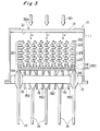
- Fig. 3 is a sectional view showing the structure of a photomultiplier according to this embodiment.
- the photomultiplier of this embodiment has a structure wherein a dynode unit 20 for multiplying an incident electron flow is disposed in a columnar vacuum vessel 10.
- the vacuum vessel 10 is constituted by a cylindrical metal side tube 11, a circular light-receiving plate 12 arranged at one end of the metal side tube 11, and a circular stem 13 forming a base portion arranged at the other end of the metal side tube 11.
- a photocathode 21 is provided on the inner surface of the light-receiving plate 12.
- An incident plane 30a where a light beam is reached is on an opposite side of the inner surface of the light-receiving plate 12.
- a focusing electrode 22 is disposed between the photocathode 21 and the dynode unit 20.
- the dynode unit 20 is constituted by stacking dynode plates 23 each having a lot of electron multiplication holes.
- a first anode component 24 for detecting the incident position of an incident plane 30a in the X direction, where the light beam is reached
- a second anode component 25 for detecting the incident position of the incident plane 30a in the Y direction, where the light beam is reached
- an inverting dynode 26 at the last stage are sequentially disposed under the dynode plates 23.
- the stem 13 serving as a base portion is connected to an external voltage terminal, through which a total of 12 stem pins 14 for applying a predetermined voltage to the dynode plates 23 and 26 extend.
- the stem pins 14 are fixed to the stem 13 through tapered hermetic glass 15.
- Each stem pin 14 has a length reaching a corresponding connected dynode.
- the distal end of each stem pin 14 is resistance-welded to the connecting terminal of the corresponding one of the dynode plates 23 and 26.
- the photoelectrons emitted from the photocathode 21 are focused onto the uppermost dynode plate 23 through the matrix-like focusing electrode 22 to be subjected to secondary multiplication.
- the secondary electrons emitted from the uppermost dynode plate 23 are applied to the lower dynode plates 23, and secondary electron emission is repeated.
- the emitted secondary electrons pass through through holes 24b and 25b of the first and second anode components 24 and 25 constituting an anode 250, and then reach the inverting dynode 26 at the last stage.
- the secondary electron group emitted from the inverting dynode 26 is captured by the first and second anode components 24 and 25.
- the captured secondary electron group is extracted from the photomultiplier through lead pins 150 individually connected to the first anode component 24 and the second anode component 25.
- the structure of this photomultiplier is disclosed in, e.g., U.S. Patent Nos. US-A-4,649,314 and US-A-4,937,506 and Japanese Patent Laid-Open Nos. JP-A-3-155036 and JP-A-5-182631.
- the anode 250 of the present invention can be applied to the photomultipliers disclosed in these prior arts.
- Fig. 4 is a perspective view showing the typical structure of the first and second anode components 24 and 25 constituting the anode 250.
- the anode components 24 and 25 are arranged parallel to the last-stage dynode 26 and kept at a potential higher than that of the dynode 26.
- the anode component 24 or 25 has a structure wherein a plurality of long metal plates 24a or 25a electrically insulated from each other are one-dimensionally aligned.
- the alignment direction of the first anode component 24 (X direction) and the alignment direction of the second anode component 25 (Y direction) are perpendicular to each other.
- Each of the metal plates 24a or 25b has the plurality of rectangular through holes 24b or 25b formed in a line.
- Secondary electrons emitted from the dynode plates 23 pass through the through holes 24b and 25b to reach the inverting dynode 26.
- the secondary electrons inverted by the dynode 26 are captured at a predetermined portion of the first and second anode components 24 and 25.
- the metal plates 24a of the first anode component 24 and the metal plates 25a of the second anode component 25 are connected to predetermined portions of resistor chains 27 outside the photomultiplier through the corresponding lead pins 150.
- Fig. 2 is a view showing the arrangement of the resistor chain 27.
- the resistor chain 27 consists of a plurality of resistors 270 connected in series.
- Each lead pin 150 having one end connected to a corresponding metal plate is connected to a corresponding portion (between the resistors 270).
- the secondary electrons captured by the first anode component 24 and the second anode component 25 and extracted from the photomultiplier through the lead pins 150 are shunted through the resistor chains 27 and extracted from terminals X 1 and X 2 and terminals Y 1 and Y 2 .
- This embodiment is characterized in that the plate-like first and second anode components 24 and 25 are arranged in place of a conventional wire anode disclosed in the above prior art. As shown in Fig. 5, these anode components 24 and 25 have a larger surface area than that of the wire anode because of having a flat surface in parallel to an electron-emitting surface of the dynode 26.
- the first anode component 24 means the X plate anode group
- the second anode component 25 means the Y plate anode group. For this reason, distortion in an equipotential line shown in Fig. 5 can be minimized, and a high field intensity can be obtained.
- the secondary electrons emitted from the dynode 26 are collected by the metal plates 24a and 25a relatively close to the emission position.
- the secondary electrons are rarely collected by the metal plates 24a and 25a far from the emission position because of stray of the secondary electrons. Therefore, crosstalk caused by stray of the secondary electrons is minimized to improve the precision of position resolving power.
- the high field intensity can prevent space-charges from being generated, resulting in good linear characteristics.
- the field intensity is high between the inverting dynode 26 and the anode 250 while a parallel field is formed therebetween to almost prevent the secondary electrons from straying, resulting in good time characteristics.
- Fig. 6 is a view showing the structure of the wire anode disclosed in the above prior art, as a comparative example.
- reference numeral 50 denotes an (n - 1)th-stage dynode
- 52 wires constituting an X wire anode group for detecting the electron capture position in the X direction and a Y wire anode group for detecting the electron capture position in the Y direction
- 51 an inverting dynode at the last stage (last-stage dynode).
- the space ratio is high, and the equipotential line is distorted. Since reflected secondary electrons emitted from the last-stage dynode 51 (inverting dynode) are diffused in a wide range, it is likely that a plurality of secondary electrons emitted from one position of the dynode 51 are extracted from different portions of the anode. This may cause crosstalk to degrade the precision of position resolving power and also increase distortion in the periphery.
- a measurement system for measuring the position resolving power of the photomultiplier will be described below with reference to Figs. 7 and 8.
- An LED is used as a light source 100.
- a light beam irradiated from this LED emerges to a photomultiplier 300 through an optical fiber 200.
- the distal end portion of the optical fiber 200 is fixed to an X-Y stage 400 so as to freely select the incident position on the photomultiplier 300.
- a predetermined voltage is applied from a voltage-dividing resistor 500 to each dynode.
- the detected electrical signals X 1 , X 2 , Y 1 , and Y 2 are amplified by a preamplifier 600, A/D-converted, and supplied to a computer 800 for calculating the incident position.
- a CRT 810 and an X-Y plotter 820 serving as a display means, and a disk driver serving as a recording means (measurement data is recorded on a floppy disk 330) are connected to the computer 800.
- the detected signals X 1 and X 2 are added by an adder 800a, and thereafter, the signal X 1 is divided by an output (X 1 + X 2 ) from the adder 800a by a divider 800b, thereby calculating the incident position of the incident light in the X direction.
- the detected signals Y 1 and Y 2 are added by an adder 800c, and thereafter, the signal Y 1 is divided by an output (Y 1 + Y 2 ) from the adder 800c by a divider 800d, thereby calculating the incident position of the incident light in the Y direction.
- Fig. 9 is a perspective view showing the manufacturing steps of the anode 250 constituted by the first and second anode components 24 and 25 attached to a ceramic frame 32.
- the first anode component 24 is attached on the upper surface of the ceramic frame 32 while the second anode component 25 is attached on the lower surface of the ceramic frame 32.
- the ceramic frame 32 has four sides 32a to 32d.
- a first end portion 24a 1 of each metal plate 24a of the first anode component 24 is fixed to the first side 32a while a second end portion 24a 2 of the metal plate 24a is fixed to the second side 32b.
- a first end portion 25a 1 of each metal plate 25a of the second anode component 25 is fixed to the third side 32c while a second end portion 25a 2 of the metal plate 25a is fixed to the fourth side 32d.
- each through hole is formed in each side of the ceramic frame 32 at an equal interval. Through holes are formed at the two ends of each of the metal plates 24a and 25a.
- the metal plates 24a are aligned with the through holes matching each other, and fixed on the upper surface of the ceramic frame 32 with eyelets.
- the metal plates 25a are aligned with the through holes matching each other, and fixed on the lower surface of the ceramic frame 32 with eyelets.
- the metal plates 24a and 25a are electrically insulated from each other by the ceramic frame 32.
- Fig. 10 is a perspective view showing the anode 250 having the above structure.
- Through holes having tapered surfaces are formed near the four apices of the ceramic frame 32.
- the ceramic frame 32 is stacked on the dynode 26 at a predetermined interval through insulating balls 31.
- the stacking direction of the dynodes 23 corresponds to the incident direction 30 of the light beam.
- Fig. 11 is a sectional view showing the multilayered structure of the dynodes 23 and 26 and the anode 250 stacked as shown in Fig. 10.
- Fig. 12 is a perspective view showing steps in manufacturing the anode 250 by using independent fixing frames (insulating bars).
- the eight metal plates 24a are parallelly aligned, and the first end portion 24a 1 and the second end portion 24a 2 of each of the metal plates 24a are attached to a first insulating bar 240a and a second insulating bar 240b, respectively.
- the eight metal plates 25a are parallelly aligned, and the first end portion 25a 1 and the second end portion 25a 2 of each of the metal plates 25a are attached to a third insulating bar 250a and a fourth insulating bar 250b, respectively.
- Through holes having tapered surfaces are formed near the four apices of each of the dynodes 23 and 26 and at the two ends of each of the four fixing frames (insulating bars 240a, 240b, 250a, and 250b). Insulating balls are placed at the positions of the through holes, positioned, and supported. For this reason, as shown in Fig. 11, the dynodes 23 and 26 and the anode components 24 and 25 are stacked at predetermined intervals, and these layers are electrically insulated from each other.
- Fig. 13 is a perspective view showing steps in manufacturing an anode 250 by bonding a first insulating plate 33 and a second insulating plate 33, each having a plurality of strip anodes (conductive thin films) deposited on the upper and lower surfaces, to a ceramic frame 32.
- the first insulating plate 33 is bonded to the upper surface of the ceramic frame 32 while the second insulating plate 34 is bonded to the lower surface of the ceramic frame 32.
- Through holes having tapered surfaces are formed near the four apices of the ceramic frame 32, and the ceramic frame 32 is stacked on the dynode 26 at a predetermined interval through insulating balls 31, as shown in Fig. 15.
- first anode component 24 eight strip anode regions 33a are parallelly aligned on the upper and lower surfaces 33d, 33e of the first insulating plate 33.
- a metal such as Al (aluminum) is deposited on the anode regions 33a.
- a plurality of rectangular anode holes 33b for passing secondary electrons are formed in a line in each anode region 33a.
- a plurality of anode regions 34a each having through holes 34b formed in a line are aligned on the upper and lower surfaces 34d, 34e of the second insulating plate 34.
- the first insulating plate 33 and the second insulating plate 34 are formed of a material such as a ceramic or glass.
- Fig. 14 shows a sectional view showing the structure of the first insulating plate 33 along A-A line in Fig. 13.
- the thin Al films of the first anode component 24 cover the entire side walls of the through holes 33b, thereby electrically connecting an upper surface 33d to a lower surface 33e of the first insulating plate 33.
- insulating regions 33c to which the surface of the first insulating plate 33 is exposed are formed between the thin Al films.
- the second anode component 25 also has the same structure.
- the two ends of the first insulating plate 33 are bonded to the upper surface of the ceramic frame 32 while the two ends of the second insulating plate 34 are bonded to the lower surface of the ceramic frame 32, thereby fixing the insulating plates.
- the alignment direction of the anode regions 33a of the first insulating plate 33 (X direction) is set to be perpendicular to the alignment direction of the anode regions 34a of the second insulating plate 34 (Y direction).
- the through holes 24b and 25b, or 33b and 34b may have another shape other than the rectangular shape, e.g., a circular or triangular shape.
- Calculation of the position of the center of gravity may be performed through hardware using the adder 28 and the divider 29, or through software such that currents output from the terminals X 1 , X 2 , Y 1 , and Y 2 are supplied to a predetermined computer through an A/D converter or the like.
- an insulating frame consisting of glass or rubber may also be used.
- the photomultiplier embodying the invention As has been described in detail, according to the photomultiplier embodying the invention, most of the plurality of electrons emitted from the inverting dynode are captured by the anode or anode regions at a portion close to the emission position. For this reason, the incident position of the electrons can be detected at a high position resolving power while minimizing the crosstalk. Particularly, since the anode component of the present invention has a large surface area for capturing the electrons, distortion in equipotential line can be minimized, and a high field intensity can be obtained. Therefore, the linear characteristics and the time characteristics can be improved.
Landscapes
- Measurement Of Radiation (AREA)
Description
Claims (14)
- An anode (250) for a photomultiplier, the anode (250) comprising:a first component (24) comprising a plurality of elongate planar conductors (24a, 33a) arranged substantially in parallel to a first axis, each planar conductor (24a, 33a) having a plurality of through holes (24b, 33b) formed along its length;a second component (25) comprising a plurality of elongate planar conductors (25a, 34a) arranged substantially in parallel to a second axis, each planar conductor (25a, 34a) having a plurality of through holes (25b, 34b) formed along its length; andsupporting means for supporting the first (24) and second (25) components with the first axis substantially orthogonal to the second axis.
- An anode (250) according to claim 1, wherein the plurality of elongate planar conductors of at least one of the first (24) and second (25) components comprises a plurality of metal plates (24a, 25a) in which said plural through holes (24b, 25b) are formed.
- An anode (250) according to claim 1, wherein the plurality of elongate planar conductors of at least one of the first (24) and second (25) components comprises a plurality of conductive thin films (33a, 34a) disposed on a surface of an insulating plate (33, 34) in which said plural through holes (33b, 34b) are formed.
- An anode (250) according to claim 1, wherein said supporting means comprises an insulating member (32, 240a, 240b, 250a, 250b), provided between said first component (24) and said second component (25) and which separates said first component (24) and second component (25) by a predetermined distance.
- An anode (250) according to claim 4, wherein the plurality of elongate planar conductor of at least one of the first (24) and second (25) component comprises a plurality of metal plates (24a, 25a) in which said plural through holes (24b, 25b) are formed.
- An anode (250) according to claim 4, wherein the plurality of elongate planar conductors of at least one of the first (24) and second (25) components comprises a plurality of conductive thin films (33a, 34a) disposed on a surface of an insulating plate (33, 34) in which said plural through holes (33b, 34b) are formed.
- An anode (250) according to claim 6, wherein each of said conductive thin films (33a, 34a) covers inner walls of said insulating plate (33, 34), which wall defines said through holes (33b, 34b).
- An anode (250) according to claim 5, wherein said insulating member comprises a frame (32) disposed between said first component (24) and said second component (25) said frame (32) having at least a first side (32a), a second side (32b) which opposes said first side (32a), and third (32c) and fourth (32d) sides which oppose each other and are in contact with said first (32a) and second (32b) sides.
- An anode (250) according to claim 8, wherein both the first (24) and second (25) components comprises a plurality of metal plates (24a, 25a), and said first side (32a) is fixed to a first end portion of each of said metal plates (24a) of said first component (24),said second side (32b) is fixed to a second end portion of each of said metal plates (24a) of said first component (24),said third side (32c) is connected to said first side (32a) and said second side (32b), and is fixed to a first end portion of each of said metal plates (25a) of said second component (25), andsaid fourth side (32d) is connected to said first side (32a) and said second side 932b), and is fixed to a second end portion of each of said metal plates (25a) of said second component (25),whereby a gap is formed between said first anode component (24) and said second anode component (25) defined by space surrounded by said sides.
- An anode (250) according to claim 5, wherein both the first (24) and second (25) components comprise a plurality of metal plates (24a, 25a), andsaid insulating member comprises:first (240a) and second (240b) insulating bars, provided between said first component (24) and said second component (25), for fixing said plurality of metal plates (24a) of said first component (24), so that a first end portion of each of said metal plates (24a) of said first component (24) is fixed to said first insulating bar (240a), and a second end portion is fixed to said second insulating bar (240b), andthird (250a) and fourth (250b) insulating bars, provided between said first component (24) and said second component (25), for fixing said plurality of metal plates (25a) of said second anode component (25) so that a first end portion of each of said metal plates (25a) of said second component (25) is fixed to said third insulating bar (250a) and a second end portion is fixed to said fourth insulating bar (250b), wherebya first end portion of said first insulating bar (240a) is fixed to a first end portion of said third insulating bar (250a), a second end portion of said first insulating bar (240a) is fixed to a first end portion of said fourth insulating bar (250b), a first end portion of said second insulating bar (240b) is fixed to a second end portion of said second insulating bar (250a), and a second end portion of said second insulating bar (240b) is fixed to a second end portion of said fourth insulating bar (250b).
- An anode (250) according to claims 6 or 7, wherein both the first (24) and second (25) components comprise a plurality of conductive thin films (33a, 34a) disposed on a surface of an insulating plate (33, 34), andsaid insulating member is an insulating frame (32) comprisinga first side (32a) on a first end portion side of said first component (24) conductive thin films (33a), to which a first end portion of said first component insulating plate (33) is fixed,a second side (32b) on a second end portion side of said first component conductive thin films (33a) which opposes said first side (32a), to which a second end portion of said first component insulating plate (33) is fixed,a third side (32c) on a first end portion side of said second component (25) conductive thin films (34a) which is connected to said first side (32a) and said second side (32b) to which a first end portion of said second component insulating plate (34) is fixed, anda fourth side (32d) on a second end portion side of said second component (25) conductive thin films (34a) which is connected to said first side and said second side, to which a second end portion of said second component (25) insulating plate (34) is fixed, whereby a gap is formed between said first component (24) and said second component (25) defined by space surrounded by said sides.
- A photomultiplier comprising:an anode (250) according to any preceding claim:a photocathode (21) for emitting photoelectrons in response to light incident thereon;a dynode unit (20) comprising a plurality of stacked dynode plates (23) for multiplying the photoelectrons; andan inverting dynode (26),wherein the anode (250) is disposed between the dynode unit (20) and the inverting dynode (26) to produce signals on the elongate planar conductors (24a, 25a, 33a, 34a) relating to the position at which light is incident on the photocathode (21).
- A photomultiplier according to claim 12, wherein the first (24) and second (25) components are connected to enable an equal potential to be applied to both.
- A photomultiplier according to claim 12 or 13, wherein in use photoelectrons multiplied by the dynode unit (20), pass through the through holes (24b, 25b, 33b, 34b) of the elongate planar conductors (24a, 25a, 33a, 34a), are incident on and multiplied by the inverting dynode (26), and electrons from the inverting dynode (26) are absorbed by the elongate planar conductors (24a, 25a, 33a, 34a) of the first (24) or second (25) component.
Applications Claiming Priority (2)
| Application Number | Priority Date | Filing Date | Title |
|---|---|---|---|
| JP199893/94 | 1994-08-24 | ||
| JP19989394A JP3445663B2 (en) | 1994-08-24 | 1994-08-24 | Photomultiplier tube |
Publications (3)
| Publication Number | Publication Date |
|---|---|
| EP0698911A2 EP0698911A2 (en) | 1996-02-28 |
| EP0698911A3 EP0698911A3 (en) | 1996-03-13 |
| EP0698911B1 true EP0698911B1 (en) | 1998-12-30 |
Family
ID=16415365
Family Applications (1)
| Application Number | Title | Priority Date | Filing Date |
|---|---|---|---|
| EP95305888A Expired - Lifetime EP0698911B1 (en) | 1994-08-24 | 1995-08-23 | Position sensitive photomultiplier |
Country Status (4)
| Country | Link |
|---|---|
| US (1) | US5637959A (en) |
| EP (1) | EP0698911B1 (en) |
| JP (1) | JP3445663B2 (en) |
| DE (1) | DE69506968T2 (en) |
Families Citing this family (13)
| Publication number | Priority date | Publication date | Assignee | Title |
|---|---|---|---|---|
| FR2748118B1 (en) * | 1996-04-24 | 1998-06-26 | Mecaserto | SCINTIGRAPHY APPARATUS |
| JP3640464B2 (en) * | 1996-05-15 | 2005-04-20 | 浜松ホトニクス株式会社 | Electron multiplier and photomultiplier tube |
| JP4146529B2 (en) * | 1997-06-11 | 2008-09-10 | 浜松ホトニクス株式会社 | Electron multiplier |
| US5880458A (en) * | 1997-10-21 | 1999-03-09 | Hamamatsu Photonics K.K. | Photomultiplier tube with focusing electrode plate having frame |
| US6452185B1 (en) * | 1999-12-16 | 2002-09-17 | Southeastern Universities Research Assn. | Method to correct energy determination in pixellated scinillation detectors |
| JP4108905B2 (en) * | 2000-06-19 | 2008-06-25 | 浜松ホトニクス株式会社 | Manufacturing method and structure of dynode |
| JP4231327B2 (en) * | 2003-04-23 | 2009-02-25 | 浜松ホトニクス株式会社 | Solid-state imaging device |
| JP2005116754A (en) * | 2003-10-07 | 2005-04-28 | Hamamatsu Photonics Kk | Semiconductor energy line detecting element |
| US7446327B2 (en) * | 2005-04-21 | 2008-11-04 | Etp Electron Multipliers Pty Ltd. | Apparatus for amplifying a stream of charged particles |
| JP4753303B2 (en) | 2006-03-24 | 2011-08-24 | 浜松ホトニクス株式会社 | Photomultiplier tube and radiation detector using the same |
| US9490911B2 (en) | 2013-03-15 | 2016-11-08 | Fairfield Industries Incorporated | High-bandwidth underwater data communication system |
| US9490910B2 (en) | 2013-03-15 | 2016-11-08 | Fairfield Industries Incorporated | High-bandwidth underwater data communication system |
| US10488537B2 (en) | 2016-06-30 | 2019-11-26 | Magseis Ff Llc | Seismic surveys with optical communication links |
Family Cites Families (12)
| Publication number | Priority date | Publication date | Assignee | Title |
|---|---|---|---|---|
| GB1490695A (en) * | 1974-10-21 | 1977-11-02 | Emi Ltd | Radiation detecting arrangements |
| US4070578A (en) * | 1976-07-30 | 1978-01-24 | Timothy John G | Detector array and method |
| FR2481004A1 (en) * | 1980-04-18 | 1981-10-23 | Hyperelec | Photo multiplier with grid anode - is formed by ladder network of coplanar spaced leaf collectors in parallel planes |
| FR2549288B1 (en) | 1983-07-11 | 1985-10-25 | Hyperelec | ELECTRON MULTIPLIER ELEMENT, ELECTRON MULTIPLIER DEVICE COMPRISING THE MULTIPLIER ELEMENT AND APPLICATION TO A PHOTOMULTIPLIER TUBE |
| JP2516995B2 (en) | 1987-08-05 | 1996-07-24 | 浜松ホトニクス株式会社 | Photomultiplier tube |
| DE3903750A1 (en) * | 1989-02-06 | 1990-08-16 | Eberhard Koehler | Anode arrangement for an electron detector, resolving in space and time, and detectors therewith |
| JPH0623670B2 (en) * | 1989-09-14 | 1994-03-30 | 浜松ホトニクス株式会社 | Photomultiplier tube |
| JP2925020B2 (en) | 1989-11-10 | 1999-07-26 | 浜松ホトニクス株式会社 | Photomultiplier tube |
| US5077504A (en) * | 1990-11-19 | 1991-12-31 | Burle Technologies, Inc. | Multiple section photomultiplier tube |
| JP3078905B2 (en) | 1991-12-26 | 2000-08-21 | 浜松ホトニクス株式会社 | Electron tube with electron multiplier |
| JP3232729B2 (en) | 1992-12-28 | 2001-11-26 | 東レ株式会社 | New peptides and antibacterial agents |
| US5572089A (en) * | 1993-04-28 | 1996-11-05 | Hamamatsu Photonics K.K. | Photomultiplier for multiplying photoelectrons emitted from a photocathode |
-
1994
- 1994-08-24 JP JP19989394A patent/JP3445663B2/en not_active Expired - Fee Related
-
1995
- 1995-08-23 EP EP95305888A patent/EP0698911B1/en not_active Expired - Lifetime
- 1995-08-23 DE DE69506968T patent/DE69506968T2/en not_active Expired - Lifetime
- 1995-08-24 US US08/518,843 patent/US5637959A/en not_active Expired - Lifetime
Also Published As
| Publication number | Publication date |
|---|---|
| EP0698911A2 (en) | 1996-02-28 |
| JPH0864168A (en) | 1996-03-08 |
| EP0698911A3 (en) | 1996-03-13 |
| DE69506968T2 (en) | 1999-06-10 |
| DE69506968D1 (en) | 1999-02-11 |
| JP3445663B2 (en) | 2003-09-08 |
| US5637959A (en) | 1997-06-10 |
Similar Documents
| Publication | Publication Date | Title |
|---|---|---|
| EP0698911B1 (en) | Position sensitive photomultiplier | |
| US5936348A (en) | Photomultiplier tube with focusing electrode plate | |
| EP0690478B1 (en) | Electron tube | |
| US4825118A (en) | Electron multiplier device | |
| US4881008A (en) | Photomultiplier with plural photocathodes | |
| US4395636A (en) | Radiation imaging apparatus | |
| US6927538B2 (en) | Photomultiplier tube | |
| GB2098796A (en) | Electron multiplier comprising microchannel plates and an amplifier dynode stage connected thereto and method of manufacturing same | |
| EP0617450B1 (en) | Streak tube | |
| EP1313133A1 (en) | Photomultiplier | |
| US5453609A (en) | Non cross talk multi-channel photomultiplier using guided electron multipliers | |
| JPS62160652A (en) | Multiplying device with high collecting efficiency, multiplier with the multiplying device, optomultiplying tubeusing the multiplying device and manufacture of multiplying device | |
| JP4402478B2 (en) | Photomultiplier tube | |
| JP2001196023A (en) | Photomultiplier | |
| US4703168A (en) | Multiplexed wedge anode detector | |
| US20040021088A1 (en) | Radiation detectors and autoradiographic imaging apparatuses comprising such detectors | |
| JPS6258536A (en) | Electron multiplying element | |
| US5880458A (en) | Photomultiplier tube with focusing electrode plate having frame | |
| JPH11329339A (en) | Photomultiplier tube and spectrometer | |
| WO2003098658A1 (en) | Photomultiplier tube and its using method | |
| EP0760525B1 (en) | Electron tube | |
| US4882480A (en) | Apparatus for detecting the position of incidence of particle beams including a microchannel plate having a strip conductor with combed teeth | |
| JPS612253A (en) | Device for detecting incidence position of secondary electrons | |
| US20230238227A1 (en) | Charged particle detector | |
| JPH08179045A (en) | Energy line detecting assembly |
Legal Events
| Date | Code | Title | Description |
|---|---|---|---|
| PUAI | Public reference made under article 153(3) epc to a published international application that has entered the european phase |
Free format text: ORIGINAL CODE: 0009012 |
|
| PUAL | Search report despatched |
Free format text: ORIGINAL CODE: 0009013 |
|
| AK | Designated contracting states |
Kind code of ref document: A2 Designated state(s): DE FR GB |
|
| AK | Designated contracting states |
Kind code of ref document: A3 Designated state(s): DE FR GB |
|
| 17P | Request for examination filed |
Effective date: 19960906 |
|
| 17Q | First examination report despatched |
Effective date: 19970523 |
|
| GRAG | Despatch of communication of intention to grant |
Free format text: ORIGINAL CODE: EPIDOS AGRA |
|
| GRAG | Despatch of communication of intention to grant |
Free format text: ORIGINAL CODE: EPIDOS AGRA |
|
| GRAH | Despatch of communication of intention to grant a patent |
Free format text: ORIGINAL CODE: EPIDOS IGRA |
|
| GRAH | Despatch of communication of intention to grant a patent |
Free format text: ORIGINAL CODE: EPIDOS IGRA |
|
| GRAA | (expected) grant |
Free format text: ORIGINAL CODE: 0009210 |
|
| AK | Designated contracting states |
Kind code of ref document: B1 Designated state(s): DE FR GB |
|
| REF | Corresponds to: |
Ref document number: 69506968 Country of ref document: DE Date of ref document: 19990211 |
|
| ET | Fr: translation filed | ||
| PLBE | No opposition filed within time limit |
Free format text: ORIGINAL CODE: 0009261 |
|
| STAA | Information on the status of an ep patent application or granted ep patent |
Free format text: STATUS: NO OPPOSITION FILED WITHIN TIME LIMIT |
|
| 26N | No opposition filed | ||
| REG | Reference to a national code |
Ref country code: GB Ref legal event code: IF02 |
|
| PGFP | Annual fee paid to national office [announced via postgrant information from national office to epo] |
Ref country code: DE Payment date: 20130821 Year of fee payment: 19 |
|
| PGFP | Annual fee paid to national office [announced via postgrant information from national office to epo] |
Ref country code: FR Payment date: 20130808 Year of fee payment: 19 Ref country code: GB Payment date: 20130821 Year of fee payment: 19 |
|
| REG | Reference to a national code |
Ref country code: DE Ref legal event code: R119 Ref document number: 69506968 Country of ref document: DE |
|
| GBPC | Gb: european patent ceased through non-payment of renewal fee |
Effective date: 20140823 |
|
| REG | Reference to a national code |
Ref country code: DE Ref legal event code: R119 Ref document number: 69506968 Country of ref document: DE Effective date: 20150303 |
|
| REG | Reference to a national code |
Ref country code: FR Ref legal event code: ST Effective date: 20150430 |
|
| PG25 | Lapsed in a contracting state [announced via postgrant information from national office to epo] |
Ref country code: DE Free format text: LAPSE BECAUSE OF NON-PAYMENT OF DUE FEES Effective date: 20150303 Ref country code: GB Free format text: LAPSE BECAUSE OF NON-PAYMENT OF DUE FEES Effective date: 20140823 |
|
| PG25 | Lapsed in a contracting state [announced via postgrant information from national office to epo] |
Ref country code: FR Free format text: LAPSE BECAUSE OF NON-PAYMENT OF DUE FEES Effective date: 20140901 |