EP0696840B1 - Régulateur à limitation de puissance - Google Patents
Régulateur à limitation de puissance Download PDFInfo
- Publication number
- EP0696840B1 EP0696840B1 EP95111950A EP95111950A EP0696840B1 EP 0696840 B1 EP0696840 B1 EP 0696840B1 EP 95111950 A EP95111950 A EP 95111950A EP 95111950 A EP95111950 A EP 95111950A EP 0696840 B1 EP0696840 B1 EP 0696840B1
- Authority
- EP
- European Patent Office
- Prior art keywords
- diode
- voltage
- power
- load
- resistor
- Prior art date
- Legal status (The legal status is an assumption and is not a legal conclusion. Google has not performed a legal analysis and makes no representation as to the accuracy of the status listed.)
- Expired - Lifetime
Links
- 230000000670 limiting effect Effects 0.000 title claims description 10
- 230000001105 regulatory effect Effects 0.000 claims description 15
- 239000004020 conductor Substances 0.000 description 13
- 230000033228 biological regulation Effects 0.000 description 4
- 230000002159 abnormal effect Effects 0.000 description 1
- 230000007423 decrease Effects 0.000 description 1
Images
Classifications
-
- H—ELECTRICITY
- H04—ELECTRIC COMMUNICATION TECHNIQUE
- H04N—PICTORIAL COMMUNICATION, e.g. TELEVISION
- H04N5/00—Details of television systems
- H04N5/63—Generation or supply of power specially adapted for television receivers
-
- G—PHYSICS
- G05—CONTROLLING; REGULATING
- G05F—SYSTEMS FOR REGULATING ELECTRIC OR MAGNETIC VARIABLES
- G05F3/00—Non-retroactive systems for regulating electric variables by using an uncontrolled element, or an uncontrolled combination of elements, such element or such combination having self-regulating properties
- G05F3/02—Regulating voltage or current
- G05F3/08—Regulating voltage or current wherein the variable is DC
- G05F3/10—Regulating voltage or current wherein the variable is DC using uncontrolled devices with non-linear characteristics
- G05F3/16—Regulating voltage or current wherein the variable is DC using uncontrolled devices with non-linear characteristics being semiconductor devices
- G05F3/18—Regulating voltage or current wherein the variable is DC using uncontrolled devices with non-linear characteristics being semiconductor devices using Zener diodes
-
- H—ELECTRICITY
- H02—GENERATION; CONVERSION OR DISTRIBUTION OF ELECTRIC POWER
- H02M—APPARATUS FOR CONVERSION BETWEEN AC AND AC, BETWEEN AC AND DC, OR BETWEEN DC AND DC, AND FOR USE WITH MAINS OR SIMILAR POWER SUPPLY SYSTEMS; CONVERSION OF DC OR AC INPUT POWER INTO SURGE OUTPUT POWER; CONTROL OR REGULATION THEREOF
- H02M3/00—Conversion of DC power input into DC power output
- H02M3/22—Conversion of DC power input into DC power output with intermediate conversion into AC
- H02M3/24—Conversion of DC power input into DC power output with intermediate conversion into AC by static converters
- H02M3/28—Conversion of DC power input into DC power output with intermediate conversion into AC by static converters using discharge tubes with control electrode or semiconductor devices with control electrode to produce the intermediate AC
- H02M3/325—Conversion of DC power input into DC power output with intermediate conversion into AC by static converters using discharge tubes with control electrode or semiconductor devices with control electrode to produce the intermediate AC using devices of a triode or a transistor type requiring continuous application of a control signal
- H02M3/335—Conversion of DC power input into DC power output with intermediate conversion into AC by static converters using discharge tubes with control electrode or semiconductor devices with control electrode to produce the intermediate AC using devices of a triode or a transistor type requiring continuous application of a control signal using semiconductor devices only
-
- H—ELECTRICITY
- H02—GENERATION; CONVERSION OR DISTRIBUTION OF ELECTRIC POWER
- H02M—APPARATUS FOR CONVERSION BETWEEN AC AND AC, BETWEEN AC AND DC, OR BETWEEN DC AND DC, AND FOR USE WITH MAINS OR SIMILAR POWER SUPPLY SYSTEMS; CONVERSION OF DC OR AC INPUT POWER INTO SURGE OUTPUT POWER; CONTROL OR REGULATION THEREOF
- H02M3/00—Conversion of DC power input into DC power output
- H02M3/22—Conversion of DC power input into DC power output with intermediate conversion into AC
- H02M3/24—Conversion of DC power input into DC power output with intermediate conversion into AC by static converters
- H02M3/28—Conversion of DC power input into DC power output with intermediate conversion into AC by static converters using discharge tubes with control electrode or semiconductor devices with control electrode to produce the intermediate AC
- H02M3/325—Conversion of DC power input into DC power output with intermediate conversion into AC by static converters using discharge tubes with control electrode or semiconductor devices with control electrode to produce the intermediate AC using devices of a triode or a transistor type requiring continuous application of a control signal
- H02M3/335—Conversion of DC power input into DC power output with intermediate conversion into AC by static converters using discharge tubes with control electrode or semiconductor devices with control electrode to produce the intermediate AC using devices of a triode or a transistor type requiring continuous application of a control signal using semiconductor devices only
- H02M3/33561—Conversion of DC power input into DC power output with intermediate conversion into AC by static converters using discharge tubes with control electrode or semiconductor devices with control electrode to produce the intermediate AC using devices of a triode or a transistor type requiring continuous application of a control signal using semiconductor devices only having more than one ouput with independent control
Definitions
- the invention relates to the field of power limiting in power supplies.
- the amount of the spacing between the conductors of a printed circuit board for consumer electronic circuits such as, for example, a television receiver, are established by regulatory organizations.
- the regulations impose strict requirements, for example, on the spacing between adjacent conductors, when at least one of the conductors is connected to an output terminal or node of a supply voltage capable of supplying more than 15 watts to a load.
- the spacing between conductors is required to be larger than when the power supply node is not capable of supplying at least 15 watts.
- Such requirements are referred to as the 15 watt node requirements.
- the larger spacing results in a larger printed circuit board area.
- a power supply in a television receiver may be required to supply a total power that is significantly greater than 15 watts.
- the power may be distributed via conductors to various circuits. Some of the circuits are low power circuits that require less than 15 watts. In order to reduce the printed circuit board area that is otherwise needed for complying with the 15 watt node requirements, it may be desirable to limit the maximum power that can be derived by such low power circuits to less than 15 watts, even when abnormal conditions such as short circuit or failure of components occur.
- a regulated power supply is energized by a DC input supply voltage.
- a first regulated voltage is produced at a first output terminal of the regulated power supply.
- the power that can be derived from the output terminal can be, for example, greater than 15 watts. Therefore, conductors that are connected directly to the output terminal are, for example, subject to the 15 watt node requirements.
- the input supply voltage is also coupled via a resistor that provides power limiting and via a clamping diode to the first output terminal of the regulated power supply.
- the diode is poled to conduct continuously in normal operation. The diode clamps or regulates a second supply voltage that is developed at a terminal of the diode, remote from the first output terminal.
- a power supply embodying an inventive feature includes a voltage regulator for applying a first regulated supply voltage to a first load.
- a power limiting impedance is used for applying a second supply voltage to a second load.
- a clamping arrangement is used for clamping the second supply voltage to the first regulated voltage to regulate the second supply voltage. Power transfer from the voltage regulator of the first supply voltage to the second load via the clamping arrangement is prevented.
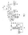
- Voltage VIN is coupled via a series-pass regulator transistor T1 to a load 111.
- a regulating base voltage VZ for transistor T1 is developed in a pair of zener diodes Z1 and Z2 that are coupled in series.
- a resistor R2 supplies a reverse current in zener diodes Z1 and Z2. Consequently, an output supply voltage VOUT1 at the emitter of transistor T1 is regulated.
- Voltage VOUT1 is developed at a supply node terminal 110 that is capable, for example, of supplying more than 15 watts.
- a level shifting and temperature compensating diode D2 couples a supply voltage VD1 developed at a terminal 113, between resistor R1 and diode D1, to a load 114 for producing an output supply voltage VOUT2.
- Voltage VOUT2 is coupled via a conductor 50 to load 114 for energizing the load.
- diode D1 In normal operation, diode D1 continuously conducts. The continuous conduction is assured by the selection of a sufficiently small value of resistor R1, such that a current IR1 in resistor R1 equals or exceeds a load current ID2 in diode D2. Therefore, voltage VOUT2 tracks and is clamped to voltage VOUT1. Diode D2 provides temperature compensation with respect to forward voltage variation of clamping diode D1. Voltage VOUT2 is approximately equal to voltage VOUT1.
- resistor R1 is chosen such that power consumption in the loads that are energized via diode D2, is less than, for example, 14 watts. Such value is selected to be smaller than 15 watts under any loading conditions via diode D2.
- a current iD1 in diode D1 cannot flow in a direction opposite to that shown by the arrow, from transistor T1 to load 114. Thus, power cannot be supplied via terminal 110 to load 114.
- the entire power supplied via diode D2, referred to as POUT2, is supplied via resistor R1. It follows that diode D1 isolates terminal 113 from terminal 110 with respect to power delivery. Because of the current or power limiting action of resistor R1, power POUT2 supplied via diode D2 is limited to less than 15 watts. Therefore, conductor 50 is not subject to the 15 watt node requirements. Consequently, advantageously, a spacing 150 between conductor 50 and any other conductor such as a conductor 51 need not meet the strict 15 watt node requirements.
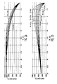
- FIGURES 2a and 2b illustrate a family of curves of voltage VOUT2 and power POUT2, respectively, as a function of resistor R1 and an equivalent load resistor RL of FIGURE 1. Similar symbols and numerals in FIGURES 1, 2a and 2b indicate similar numbers or functions.
- Resistor RL of FIGURE 1 represents the entire or equivalent load that is energized via diode D2.
- Power POUT2 is the entire power that is dissipated in the load represented by resistor RL as a result of the current in diode D2.
- voltage VOUT2 varies by less than 10% over a substantially large range of variation of load.
- power POUT2 cannot exceed 14 watts for an entire range of values of resistors RL and R1 of FIGURE 1.
- voltage VOUT2 decreases such that diode D1 becomes non-conductive.
- Diode D1 prevents power transfer from transistor T1 to, for example, load 114. In this way, diode D1 prevents transistor T1 from supplying any portion of power POUT2.
- terminal 113, diode D2 and conductor 50 are not subject to the 15 watt node requirements.
- terminal 110 may be subject to the 15 watt node requirements. This is so because diode D1 prevents power transfer from transistor T1 to, for example, load 114.
Landscapes
- Engineering & Computer Science (AREA)
- Power Engineering (AREA)
- Physics & Mathematics (AREA)
- Radar, Positioning & Navigation (AREA)
- Electromagnetism (AREA)
- General Physics & Mathematics (AREA)
- Nonlinear Science (AREA)
- Automation & Control Theory (AREA)
- Multimedia (AREA)
- Signal Processing (AREA)
- Direct Current Feeding And Distribution (AREA)
- Continuous-Control Power Sources That Use Transistors (AREA)
- Control Of Electrical Variables (AREA)
- Dc-Dc Converters (AREA)
- Television Receiver Circuits (AREA)
Claims (6)
- Une alimentation de puissance, comportant:caractérisée par :un régulateur de tension (T1, Z1, Z2) ayant une entrée couplée à une source (VIN) de tension d'alimentation d'entrée pour appliquer une première tension d'alimentation régulée (VOUT1) à une première charge (111);une impédance de limitation de puissance (R1) connectée à ladite source (VIN) pour appliquer une seconde tension d'alimentation (VD1) à une seconde charge (114);une première diode (D1) ayant une première borne (113) couplée à ladite impédance et une seconde borne (110) couplée à ladite première tension d'alimentation régulée pour réguler ladite seconde tension d'alimentation en limitant ladite seconde tension d'alimentation à ladite première tension d'alimentation et pour isoler ledit régulateur de tension de ladite seconde charge de manière à empêcher ledit régulateur de tension d'alimenter ladite seconde charge.
- Une alimentation selon la revendication 1 comprenant de plus une seconde diode qui est couplée entre ladite seconde charge et ladite première diode pour fournir une compensation de température par rapport aux variations dans ladite première diode.
- Une alimentation selon la revendication 1, caractérisée en ce que ladite impédance (R1) comporte une résistance.
- Une alimentation selon la revendication 1, caractérisée en ce que ladite première diode (D1) et ladite résistance (R1) sont couplées en séries.
- Une alimentation selon la revendication 2, caractérisée en ce que ladite seconde diode (D2) est couplée en séries avec ladite résistance (R1) et entre ladite résistance et ladite seconde charge (114).
- Une alimentation de puissance selon la revendication 1, caractérisée en ce que ledit régulateur (T1, Z1, Z2) comporte un régulateur de passage en séries.
Applications Claiming Priority (2)
| Application Number | Priority Date | Filing Date | Title |
|---|---|---|---|
| US08/287,591 US5604425A (en) | 1994-08-08 | 1994-08-08 | Power limiting regulator |
| US287591 | 1994-08-08 |
Publications (3)
| Publication Number | Publication Date |
|---|---|
| EP0696840A2 EP0696840A2 (fr) | 1996-02-14 |
| EP0696840A3 EP0696840A3 (fr) | 1996-05-29 |
| EP0696840B1 true EP0696840B1 (fr) | 1999-06-16 |
Family
ID=23103562
Family Applications (1)
| Application Number | Title | Priority Date | Filing Date |
|---|---|---|---|
| EP95111950A Expired - Lifetime EP0696840B1 (fr) | 1994-08-08 | 1995-07-29 | Régulateur à limitation de puissance |
Country Status (7)
| Country | Link |
|---|---|
| US (1) | US5604425A (fr) |
| EP (1) | EP0696840B1 (fr) |
| JP (1) | JPH0883130A (fr) |
| KR (1) | KR100341974B1 (fr) |
| CN (1) | CN1048121C (fr) |
| AU (1) | AU687216B2 (fr) |
| DE (1) | DE69510283T2 (fr) |
Families Citing this family (7)
| Publication number | Priority date | Publication date | Assignee | Title |
|---|---|---|---|---|
| TW349287B (en) * | 1996-09-12 | 1999-01-01 | Thomson Consumer Electronics | A forward converter with an inductor coupled to a transformer winding |
| FR2821306B1 (fr) * | 2001-02-26 | 2007-10-19 | Valeo Vision | Dispositif d'alimentation pour composants electriques installes dans un vehicule automobile |
| US6792338B2 (en) * | 2001-04-06 | 2004-09-14 | Honeywell International, Inc. | System and method for actively limiting the power drawn from a power distribution bus |
| US20070291126A1 (en) * | 2006-06-20 | 2007-12-20 | Matsushita Electric Industrial Co., Ltd. | Camera with interchangeable lenses having electrical circuitry |
| US9071073B2 (en) * | 2007-10-04 | 2015-06-30 | The Gillette Company | Household device continuous battery charger utilizing a constant voltage regulator |
| KR20100119043A (ko) * | 2009-04-30 | 2010-11-09 | 삼성전자주식회사 | 광원 구동 방법, 이를 수행하기 위한 광원 구동 장치 및 이를 포함하는 표시 장치 |
| CN103078605A (zh) * | 2012-11-04 | 2013-05-01 | 王少夫 | 一种高频超宽带功率限制器设计方法 |
Family Cites Families (25)
| Publication number | Priority date | Publication date | Assignee | Title |
|---|---|---|---|---|
| US2976475A (en) * | 1957-04-08 | 1961-03-21 | Gen Electric | Electrical signal regulator |
| US3182246A (en) * | 1960-09-30 | 1965-05-04 | Gen Mills Inc | Electrical power supply regulator system |
| US3174093A (en) * | 1961-01-11 | 1965-03-16 | Martin J Finkelstein | Regulated power supply systems |
| US3214668A (en) * | 1962-12-04 | 1965-10-26 | Gen Devices Inc | Transistorized voltage regulator |
| US3201606A (en) * | 1962-12-21 | 1965-08-17 | Itt | Overload protection in transistorized power regulating circuits |
| US3624490A (en) * | 1964-02-05 | 1971-11-30 | Rca Corp | Two terminal current regulator |
| US3461376A (en) * | 1966-02-14 | 1969-08-12 | Wanlass Electric Co | Ac solid state voltage regulator |
| US3431486A (en) * | 1966-10-28 | 1969-03-04 | Motorola Inc | Protection circuit including power dissipation limiting means |
| US3579039A (en) * | 1969-02-17 | 1971-05-18 | Scm Corp | Surge protection circuit |
| US3961208A (en) * | 1974-02-11 | 1976-06-01 | Litton Business Systems, Inc. | Temperature compensation for regulator circuit |
| JPS568007Y2 (fr) * | 1975-04-16 | 1981-02-21 | ||
| US4298892A (en) * | 1978-12-13 | 1981-11-03 | Rca Corporation | Switching regulator with independent feedback path filter |
| JPS5632214U (fr) * | 1979-08-11 | 1981-03-30 | ||
| US4290004A (en) * | 1980-02-04 | 1981-09-15 | Emhart Industries, Inc. | Voltage regulator circuit |
| US4488106A (en) * | 1982-07-01 | 1984-12-11 | Alan Chernotsky | Resettable power limiting apparatus |
| US4884161A (en) * | 1983-05-26 | 1989-11-28 | Honeywell, Inc. | Integrated circuit voltage regulator with transient protection |
| US4636709A (en) * | 1983-07-29 | 1987-01-13 | Sony Corporation | Regulated DC power supply |
| US4521725A (en) * | 1983-12-02 | 1985-06-04 | United Technologies Corporation | Series switching regulator |
| JPH0668706B2 (ja) * | 1984-08-10 | 1994-08-31 | 日本電気株式会社 | 基準電圧発生回路 |
| US4761723A (en) * | 1987-02-27 | 1988-08-02 | Rca Licensing Corporation | Power supply regulator for television |
| US4837653A (en) * | 1987-06-26 | 1989-06-06 | Data I/O Corporation | Quasi-power measurement circuit |
| US4945465A (en) * | 1988-09-15 | 1990-07-31 | U.S. Philips Corporation | Switched-mode power supply circuit |
| US5087870A (en) * | 1989-10-05 | 1992-02-11 | Hewlett-Packard Company | Constant power circuit |
| DE69314688T2 (de) * | 1992-04-23 | 1998-02-19 | Heidenhain Gmbh Dr Johannes | Numerische Steuerungseinrichtung und Verfahren zur Steuerung der Bewegung eines Werkzeuges |
| US5412308A (en) * | 1994-01-06 | 1995-05-02 | Hewlett-Packard Corporation | Dual voltage power supply |
-
1994
- 1994-08-08 US US08/287,591 patent/US5604425A/en not_active Expired - Fee Related
-
1995
- 1995-07-29 EP EP95111950A patent/EP0696840B1/fr not_active Expired - Lifetime
- 1995-07-29 DE DE69510283T patent/DE69510283T2/de not_active Expired - Fee Related
- 1995-08-03 KR KR1019950023932A patent/KR100341974B1/ko not_active Expired - Fee Related
- 1995-08-04 JP JP7219826A patent/JPH0883130A/ja active Pending
- 1995-08-07 CN CN95109847A patent/CN1048121C/zh not_active Expired - Fee Related
- 1995-08-07 AU AU28395/95A patent/AU687216B2/en not_active Ceased
Also Published As
| Publication number | Publication date |
|---|---|
| EP0696840A2 (fr) | 1996-02-14 |
| KR960009685A (ko) | 1996-03-22 |
| EP0696840A3 (fr) | 1996-05-29 |
| KR100341974B1 (ko) | 2002-11-02 |
| US5604425A (en) | 1997-02-18 |
| CN1048121C (zh) | 2000-01-05 |
| CN1122965A (zh) | 1996-05-22 |
| AU687216B2 (en) | 1998-02-19 |
| DE69510283D1 (de) | 1999-07-22 |
| DE69510283T2 (de) | 1999-10-14 |
| JPH0883130A (ja) | 1996-03-26 |
| AU2839595A (en) | 1996-02-22 |
Similar Documents
| Publication | Publication Date | Title |
|---|---|---|
| US6643148B1 (en) | Audio band conducted emissions suppression on power feeders | |
| US5459652A (en) | Boot strap circuit for power up control of power supplies | |
| EP1383033B1 (fr) | Circuit de limitation de puissance à retard | |
| US6992404B2 (en) | Line powering of auxiliary equipment | |
| US4937722A (en) | High efficiency direct coupled switched mode power supply | |
| US5005112A (en) | Regulated D.C.-D.C. power converter having multiple D.C. outputs | |
| US5604425A (en) | Power limiting regulator | |
| US4371919A (en) | Load distribution among parallel DC-DC converters | |
| US6005303A (en) | Linear voltage regulator compatible with bipolar and MOSFET pass devices and associated methods | |
| US5122945A (en) | Voltage controlled preload | |
| US6201374B1 (en) | Voltage regulation and power switching system | |
| US20050173988A1 (en) | Input power sharing | |
| US5377093A (en) | Current sensing circuit of a switching mode power supply | |
| US6611436B2 (en) | Switching power supply unit having a regulator circuit and electronic apparatus using the same | |
| US4476351A (en) | Subscriber loop current regulator | |
| US5502634A (en) | Regulated auxiliary power supply | |
| KR970006662B1 (ko) | 텔레비젼 장치 및 그 전원 | |
| GB2197095A (en) | Regulator for isolated chassis power supply | |
| KR100296577B1 (ko) | 전원공급장치의 출력전압 안정화회로 | |
| US5838557A (en) | Circuit for use in a DC-DC converter having a booster module | |
| EP0316147B1 (fr) | Circuit et procédé d'attaque à gain élevé | |
| CA2010004C (fr) | Circuit d'adaptation d'impedance | |
| KR0134331Y1 (ko) | 다출력 스위칭 모드 전원공급회로의 출력안정화회로 | |
| JPH05122934A (ja) | スイツチング式直流電源装置 | |
| GB2225911A (en) | Relay drive circuit regulates voltage across relay coil |
Legal Events
| Date | Code | Title | Description |
|---|---|---|---|
| PUAI | Public reference made under article 153(3) epc to a published international application that has entered the european phase |
Free format text: ORIGINAL CODE: 0009012 |
|
| AK | Designated contracting states |
Kind code of ref document: A2 Designated state(s): DE FR GB IT |
|
| PUAL | Search report despatched |
Free format text: ORIGINAL CODE: 0009013 |
|
| AK | Designated contracting states |
Kind code of ref document: A3 Designated state(s): DE FR GB IT |
|
| 17P | Request for examination filed |
Effective date: 19961102 |
|
| 17Q | First examination report despatched |
Effective date: 19970617 |
|
| GRAG | Despatch of communication of intention to grant |
Free format text: ORIGINAL CODE: EPIDOS AGRA |
|
| GRAG | Despatch of communication of intention to grant |
Free format text: ORIGINAL CODE: EPIDOS AGRA |
|
| GRAH | Despatch of communication of intention to grant a patent |
Free format text: ORIGINAL CODE: EPIDOS IGRA |
|
| GRAH | Despatch of communication of intention to grant a patent |
Free format text: ORIGINAL CODE: EPIDOS IGRA |
|
| GRAA | (expected) grant |
Free format text: ORIGINAL CODE: 0009210 |
|
| AK | Designated contracting states |
Kind code of ref document: B1 Designated state(s): DE FR GB IT |
|
| REF | Corresponds to: |
Ref document number: 69510283 Country of ref document: DE Date of ref document: 19990722 |
|
| ET | Fr: translation filed | ||
| PLBE | No opposition filed within time limit |
Free format text: ORIGINAL CODE: 0009261 |
|
| STAA | Information on the status of an ep patent application or granted ep patent |
Free format text: STATUS: NO OPPOSITION FILED WITHIN TIME LIMIT |
|
| 26N | No opposition filed | ||
| REG | Reference to a national code |
Ref country code: GB Ref legal event code: IF02 |
|
| REG | Reference to a national code |
Ref country code: FR Ref legal event code: D6 |
|
| REG | Reference to a national code |
Ref country code: GB Ref legal event code: 746 Effective date: 20030103 |
|
| PGFP | Annual fee paid to national office [announced via postgrant information from national office to epo] |
Ref country code: GB Payment date: 20050531 Year of fee payment: 11 |
|
| PGFP | Annual fee paid to national office [announced via postgrant information from national office to epo] |
Ref country code: FR Payment date: 20050705 Year of fee payment: 11 |
|
| PGFP | Annual fee paid to national office [announced via postgrant information from national office to epo] |
Ref country code: DE Payment date: 20050720 Year of fee payment: 11 |
|
| PG25 | Lapsed in a contracting state [announced via postgrant information from national office to epo] |
Ref country code: GB Free format text: LAPSE BECAUSE OF NON-PAYMENT OF DUE FEES Effective date: 20060729 |
|
| PGFP | Annual fee paid to national office [announced via postgrant information from national office to epo] |
Ref country code: IT Payment date: 20060731 Year of fee payment: 12 |
|
| PG25 | Lapsed in a contracting state [announced via postgrant information from national office to epo] |
Ref country code: DE Free format text: LAPSE BECAUSE OF NON-PAYMENT OF DUE FEES Effective date: 20070201 |
|
| GBPC | Gb: european patent ceased through non-payment of renewal fee |
Effective date: 20060729 |
|
| REG | Reference to a national code |
Ref country code: FR Ref legal event code: ST Effective date: 20070330 |
|
| PG25 | Lapsed in a contracting state [announced via postgrant information from national office to epo] |
Ref country code: FR Free format text: LAPSE BECAUSE OF NON-PAYMENT OF DUE FEES Effective date: 20060731 |
|
| PG25 | Lapsed in a contracting state [announced via postgrant information from national office to epo] |
Ref country code: IT Free format text: LAPSE BECAUSE OF NON-PAYMENT OF DUE FEES Effective date: 20070729 |