EP0696066A2 - Schaltungs-Halbleiterbauteil und Leistungswandler - Google Patents
Schaltungs-Halbleiterbauteil und Leistungswandler Download PDFInfo
- Publication number
- EP0696066A2 EP0696066A2 EP95304623A EP95304623A EP0696066A2 EP 0696066 A2 EP0696066 A2 EP 0696066A2 EP 95304623 A EP95304623 A EP 95304623A EP 95304623 A EP95304623 A EP 95304623A EP 0696066 A2 EP0696066 A2 EP 0696066A2
- Authority
- EP
- European Patent Office
- Prior art keywords
- semiconductor layer
- layer
- semiconductor
- gate
- voltage
- Prior art date
- Legal status (The legal status is an assumption and is not a legal conclusion. Google has not performed a legal analysis and makes no representation as to the accuracy of the status listed.)
- Withdrawn
Links
- 239000004065 semiconductor Substances 0.000 title claims abstract description 147
- 239000012535 impurity Substances 0.000 claims abstract description 112
- 239000000758 substrate Substances 0.000 claims abstract description 12
- 239000000969 carrier Substances 0.000 claims description 18
- 230000001419 dependent effect Effects 0.000 claims 1
- 230000000903 blocking effect Effects 0.000 description 88
- 230000005684 electric field Effects 0.000 description 24
- 238000009826 distribution Methods 0.000 description 21
- 230000000694 effects Effects 0.000 description 18
- 238000009792 diffusion process Methods 0.000 description 14
- 230000007423 decrease Effects 0.000 description 13
- 229910021332 silicide Inorganic materials 0.000 description 11
- FVBUAEGBCNSCDD-UHFFFAOYSA-N silicide(4-) Chemical compound [Si-4] FVBUAEGBCNSCDD-UHFFFAOYSA-N 0.000 description 11
- 230000015556 catabolic process Effects 0.000 description 10
- 238000002347 injection Methods 0.000 description 8
- 239000007924 injection Substances 0.000 description 8
- 230000007246 mechanism Effects 0.000 description 6
- 230000004048 modification Effects 0.000 description 6
- 238000012986 modification Methods 0.000 description 6
- 230000002093 peripheral effect Effects 0.000 description 6
- VYPSYNLAJGMNEJ-UHFFFAOYSA-N Silicium dioxide Chemical compound O=[Si]=O VYPSYNLAJGMNEJ-UHFFFAOYSA-N 0.000 description 5
- 230000009545 invasion Effects 0.000 description 5
- 239000011347 resin Substances 0.000 description 5
- 229920005989 resin Polymers 0.000 description 5
- 229910052814 silicon oxide Inorganic materials 0.000 description 5
- 239000004411 aluminium Substances 0.000 description 4
- 229910052782 aluminium Inorganic materials 0.000 description 4
- XAGFODPZIPBFFR-UHFFFAOYSA-N aluminium Chemical compound [Al] XAGFODPZIPBFFR-UHFFFAOYSA-N 0.000 description 4
- 230000008901 benefit Effects 0.000 description 4
- 230000003247 decreasing effect Effects 0.000 description 4
- 238000010586 diagram Methods 0.000 description 4
- 230000009931 harmful effect Effects 0.000 description 4
- 238000004519 manufacturing process Methods 0.000 description 4
- 238000005036 potential barrier Methods 0.000 description 4
- 230000002441 reversible effect Effects 0.000 description 4
- 229910052710 silicon Inorganic materials 0.000 description 4
- XUIMIQQOPSSXEZ-UHFFFAOYSA-N Silicon Chemical compound [Si] XUIMIQQOPSSXEZ-UHFFFAOYSA-N 0.000 description 3
- 239000000654 additive Substances 0.000 description 3
- 230000015572 biosynthetic process Effects 0.000 description 3
- 230000006866 deterioration Effects 0.000 description 3
- 238000001312 dry etching Methods 0.000 description 3
- 230000006872 improvement Effects 0.000 description 3
- 230000006698 induction Effects 0.000 description 3
- 238000000034 method Methods 0.000 description 3
- 239000010703 silicon Substances 0.000 description 3
- 239000006185 dispersion Substances 0.000 description 2
- 239000000463 material Substances 0.000 description 2
- 229910052751 metal Inorganic materials 0.000 description 2
- 239000002184 metal Substances 0.000 description 2
- 230000003071 parasitic effect Effects 0.000 description 2
- 238000002161 passivation Methods 0.000 description 2
- 230000000149 penetrating effect Effects 0.000 description 2
- GYHNNYVSQQEPJS-UHFFFAOYSA-N Gallium Chemical compound [Ga] GYHNNYVSQQEPJS-UHFFFAOYSA-N 0.000 description 1
- 239000004642 Polyimide Substances 0.000 description 1
- 229910008479 TiSi2 Inorganic materials 0.000 description 1
- 230000004888 barrier function Effects 0.000 description 1
- DFJQEGUNXWZVAH-UHFFFAOYSA-N bis($l^{2}-silanylidene)titanium Chemical compound [Si]=[Ti]=[Si] DFJQEGUNXWZVAH-UHFFFAOYSA-N 0.000 description 1
- 239000003990 capacitor Substances 0.000 description 1
- 238000007796 conventional method Methods 0.000 description 1
- 238000005520 cutting process Methods 0.000 description 1
- 230000008021 deposition Effects 0.000 description 1
- 230000003292 diminished effect Effects 0.000 description 1
- 230000008034 disappearance Effects 0.000 description 1
- 238000010894 electron beam technology Methods 0.000 description 1
- 238000005530 etching Methods 0.000 description 1
- 238000000605 extraction Methods 0.000 description 1
- 229910052733 gallium Inorganic materials 0.000 description 1
- 230000005251 gamma ray Effects 0.000 description 1
- 238000003754 machining Methods 0.000 description 1
- 230000007257 malfunction Effects 0.000 description 1
- 230000005012 migration Effects 0.000 description 1
- 238000013508 migration Methods 0.000 description 1
- 238000012858 packaging process Methods 0.000 description 1
- 229920001721 polyimide Polymers 0.000 description 1
- 230000008569 process Effects 0.000 description 1
- 238000012545 processing Methods 0.000 description 1
- 230000001681 protective effect Effects 0.000 description 1
- 230000005855 radiation Effects 0.000 description 1
- 230000006798 recombination Effects 0.000 description 1
- 238000005215 recombination Methods 0.000 description 1
- 230000002829 reductive effect Effects 0.000 description 1
- 230000000087 stabilizing effect Effects 0.000 description 1
- 230000003068 static effect Effects 0.000 description 1
- 229910021341 titanium silicide Inorganic materials 0.000 description 1
Images


Classifications
-
- H—ELECTRICITY
- H10—SEMICONDUCTOR DEVICES; ELECTRIC SOLID-STATE DEVICES NOT OTHERWISE PROVIDED FOR
- H10D—INORGANIC ELECTRIC SEMICONDUCTOR DEVICES
- H10D18/00—Thyristors
- H10D18/60—Gate-turn-off devices
Definitions
- the present invention relates to a semiconductor device particularly suitable to the use in high frequencies and in a large power equipment.
- GTO Gate Turn Off
- SI Static Induction
- the power loss generated in the device when switched that is, the switching loss increases in proportion to the frequency.
- a turn-off loss that is, the loss made when a current is turned off, which occupies a large part of the switching loss.
- it is effective to cut off the life time of carriers by emitting an electron beam or a ⁇ ray to the device so as to speed up the disappearance of the carriers.
- the life time is cut off, the amount of the carriers in a stationary on-state is decreased.
- the GTO has a p base layer with high impurity concentration. If the life time of carriers is cut off to a certain extent, that of the carriers in the p base layer also becomes short. Therefore, the number of electrons extremely decreases, which is injected from a cathode and can arrive at an n base layer through the p base layer. Accordingly, even if the turn-off loss can be decreased to a certain extent, an undesirable effect such as the sudden increasement of the on-voltage occurs strongly with it. While, because the SI thyristor has not the p base layer with the high impurity concentration, it is possible to decrease the turn-off loss by cutting off the life time, with suppressing the increasement of the on-voltage.
- the loss becomes lower.
- the blocking voltage of a thyristor with a high blocking voltage of which the rated voltage is more than 4.5 kV. Because the SI thyristor has not the layer corresponding to the p base layer of the GTO, an anode voltage is blocked by forming an negative potential barrier in a channel due to a gate potential. Therefore, if a high inverese bias voltage is not applied to the gate, the high anode voltage can be blocked. In addition, because the SI thyristor has not the layer corresponding to the p base layer of the GTO and it is impossible to accept the anode voltage by a horizontal pn junction, it is difficult to make a device with a high blocking voltage.
- the width of the channel may effect greatly on the blocking voltage.
- the dispersion of the work of the p-type gate layer may affect greatly on the blocking voltage. If there is such a portion in the device where the blocking voltage is low, the blocking voltage of the whole device may be limited within that of the portion. It is, therefore, difficult to obtain the desired blocking voltage with good yield.
- the present invention is made under the consideration of the above-mentioned problems.
- An object of the present invention is to provide a semiconductor device which has both the characteristics of a high blocking voltage and a lower loss.
- the concentration of impurities designates an absolute value of the difference between the concentration of acceptor impurities and that of donor impurities, the substantial concentration of impurities. Further, the total amount of impurities designates the amount corresponding to the substantial concentration of impurities.
- a semiconductor device of the present invention is provided with a semiconductor substrate which includes a pair of main surfaces, a first semiconductor layer of a first conductivity type adjacent to one of the main surface, a second semiconductor layer of a second conducting type of which impurity concentration is lower than that of the first semiconductor layer and which is adjacent to the first semiconductivity, a third semiconductor layer of the first conductivity type adjacent to the second semiconductor, and a fourth semiconductor of the second conductivity type of which impurity concentration is higher than that of the third semiconductor and which is adjacent to the other of the main surfaces and the third semiconductor.
- the semiconductor device further includes one main electrode in ohmic-contact with the first semiconductor layer on one of the main surfaces of said semiconductor substrate, the other main electrode in ohmic-contact with the first semiconductor layer on-the other of the main surfaces of said semiconductor substrate, and a control electrode connected electrically to the third semiconductor layer.
- the total amount of impurities of said third semiconductor layer between said second semiconductor layer and said fourth semiconductor layer is less than 1014cm ⁇ .
- the total amount of the impurities of the third semiconductor layer between the second semiconductor layer and the fourth semiconductor layer is in the range of 101cm ⁇ to 1014cm ⁇ .
- the present invention it is possible to improve the blocking voltage, because the applied voltage can be blocked by a junction of the second semiconductor layer of the first conductivity type and the third semiconductor layer of the second conductivity type in an off-state. It is further possible to increase the amount of carriers injected from the fourth semiconductor layer to the second semiconductor layer, because the transport factor of the carriers is improved in the third semiconductor layer by setting the total amount of the impurities of the third semiconductor so as to be less than 1014cm ⁇ 2, which is provided between the second semiconductor layer and the fourth semiconductor layer. As a result, it becomes possible to suppress the on-voltage so as to be low due to the cut-off of the lifetime of the carriers, even if the turn-off loss is decreased. Namely, the semiconductor device according to the present invention has both the characteristics of a low on-voltage and a low turn-off loss.
- the total amount of the impurities of the third semiconductor layer between the second semiconductor layer and the fourth semiconductor layer is in the range of 101cm ⁇ 2 to 1014cm ⁇ 2. It is possible to block a voltage regardless of the presence or absence of a signal or the polarity of a control electrode, by setting the total amount of the impurities of the third semiconductor layer so as to be equal to or more than 101cm ⁇ , and obtain a normally-off characteristic.
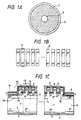
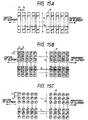
- Fig.1A is a plan view of the whole device of a recess gate type according to a first embodiment of the present invention.
- Fig.1B is a plan view of a segment of the recess gate type device.
- Fig.1C is a sectional view of a segment of the recess gate type device.
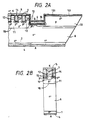
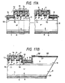
- Fig.2A is a sectional view of a peripheral region of the recess gate type device according to the first embodiment of the present invention.
- Fig.2B is a sectional view of a unit element.
- Figs.3A to 3F are sectional views of the neighborhood of a cathode of the unit element.
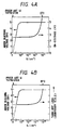
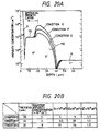
- Fig.4A is a graph representing the relationship between the total amount Q of the impurities and the anode blocking voltage and that between the total amount Q and the on-voltage.
- Fig.4B is a graph representing the relationship between the total amount Q of the impurities and the anode blocking voltage and that between the total amount Q and the turn-off loss.
- Fig.5 is a graph representing the relationship between the total amount Q of impurities and the anode blocking voltage.
- Figs.6A and 6B are schematic views illustrating an inner state of the device short-circuited between the gate and the cathode.
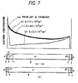
- Fig.7 is a graph representing the distribution of the impurity concentration in the vertical direction of the device or element and that of the electron concentration at the normally-on of the device.
- Fig.8 is a graph representing the relationship between an on-voltage and a turn-off loss.
- Figs.9A to 9J each is a schematic view of the step of a manufacturing process of the device.
- Figs.10A and 10B are a gragh and a table showing an example of the impurity distribution of a p- layer produced by using the manufacturing process shown in Figs.9A to 9J and conditions thereof, respectively.
- Figs.11A is a graph representing the relationship between the total amount Q' of impurities and the anode blocking voltage.
- Figs.11B is a graph representing the relationship between the total amount Q'' of impurities and the anode blocking voltage.
- Figs.11C is a graph representing the relationship between the anode blocking voltage and the dimension I2 of a p+ layer, and that between the on-voltage and the dimension I2.
- Figs.12A to 12C are illustrations of the mechanism of Fig.11A.
- Figs.13A to 13C are illustrations of the mechanism of Fig.11B.
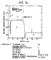
- Fig.14 is a graph representing the impurity distribution in a modification of the first embodiment.
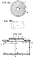
- Figs.15A to 15C are views each showing a plane pattern of a cathode n+ layer.
- Figs.16A and 16B are views showing a modification of the first embodiment.
- Figs.17A and 17B are views showing an example in which a silicide layer is inserted between an anode p layer and an aluminium layer of an anode electrode in Fig.16.
- Figs.18A to 18C are views showing an element of a buried gate type according to a second embodiment.
- Figs.19A to 19C are views showing an element of a buried gate type according to a second embodiment.
- Figs.20A and 20B are a gragh and a table showing an example of the impurity distribution of a p- layer and conditions thereof, respectively.
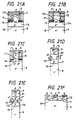
- Figs.21A to 21F are views showing other embodiments of the present invention.
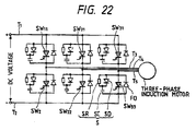
- Fig.22 is a circuit diagram showing an example of a power converter using the semiconductor device according to the present invention.
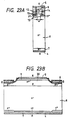
- Fig.23A is a schematic view showing a conventional recessed gate type SI thyristor.
- Fig.23B is a schematic view showing a conventional GTO.
- Figs.1 and 2 show the structure of a 4.5 kV device or element according to an embodiment of the present invention.
- Fig.1A shows a schematic plane pattern
- Fig.1B a sub-unit of a semiconductor device or the plane pattern of a segment
- Fig.1C a schematic sectional view of the structure of the segment.
- Fig.2A shows a schematic sectional view of the structure of the periphery portion of the device
- Fig.2B the minimum unit of the semiconductor device forming a segment or a schematic sectional view of the unit device.
- a hatched part 1 has a segment and a gate wiring region.
- a plurality of segments are arranged radially toward the center of a circle.
- Numeral 2 designates a gate electrode.
- the gate wiring in the hatch part 1 is connected to the gate electrode, and pass the gate current through the gate electrode.
- Numeral 3 is a peripheral region required to obtain the necessary blocking voltage.
- a gate is provided on the bottom of a groove 12 like this.
- the device of a recessed gate type will be referred to as a first embodiment.
- Numeral 4 designates an anode electrode (a first main electrode), and 5 a cathode electrode (a second main electrode).
- a gate wiring 6 connected to the gate electrode 2 is provided in the periphery of the segment.
- the gate wiring 6 functions as a gate electrode to the segment, and is therefore called also a gate electrode (a control electrode).
- Numeral 7 designates a p+ layer (a first semiconductor layer) for injecting holes, numeral 8 n- layer (a second semiconductor layer) with the impurity concentration lower than that of p+ layer 7, numeral 9 n+ layer (a fourth semiconductor layer) for injecting electrons, numeral 10 a p+ layer of the gate (a fifth semiconductor layer), and numeral 11 p- layer (a third semiconductor layer).
- the p- layer 11 isolates the n- layer 8 from the gate p+ layer 10 and the cathode n+ layer 9.
- the total amount of the impurities of the p- layer 11 between the n- layer 8 and the n+ layer 9 should be at least less than 1014cm ⁇ .
- the pn junction 18 of the p- layer 11 and n- layer 8 is in a plane form, and an anode short-circuit structure is adopted.
- a groove 12 is provided for forming a gate portion and is filled with a resin 13 such as polyimide.
- Numeral 14 designates a silicon oxide provided for stabilizing the characteristic of the surface of the side wall of the groove.
- Numeral 15 designates a silicide layer with a low resistance which functions as the gate wiring in the segment, and 16 a resin layer for passivation of the device.
- TiSi2 titanium silicide
- the segment has the structure in which a plurality of smaller unit devices 17 are arranged.
- Fig.2B shows a section of the unit device.
- Fig.23A is a sectional view showing the unit device of a conventional recessed gate type SI thyristor
- Fig.23B is a sectional view showing the unit device of a conventional GTO.
- the conventional SI thyristor has not the p- layer 11 and the p layer 30 of a conventional GTO has large total amount of the impurities and the impurity concentration higher than that of the p- layer 11 of the present embodiment.
- Fig.3 shows a section in the neighborhood of the cathode 5 of the unit device 17.
- the definition of the area of the gate p+ layer 10 of the present embodiment will be explained with reference to Fig.3.
- the gate p+ layer 10 is formed as a gate layer, has the same conductivity type as the p- layer 11, but has the impurity concentration higher than that of the p- layer 11. Namely, the magnitude of the impurity concentration in this region can not be disregarded compared with the p- layer 11.
- the following definition is made in consideration of the above matter.
- Fig.3A is an enlarged view showing the neighborhood of a gate wiring layer 15.
- the maximum impurity concentration of the gate p+ layer 10 of the gate adjacent to the gate wiring layer 15 is basically larger than 1 x 1018cm ⁇ 3.
- the impurity concentration in region 20 is 1/10 of the maximum impurity concentration.
- the distance is set to I1, which measured from the bottom of the groove 12 to the position nearest to the n- layer 8 of the region 20 (in this case, it is in plane).
- the gate p+ layer 10 is formed within the region where the distance I2 from the bottom of the groove 12 is smaller than 3 x I2.
- Fig.3B shows the definition of channel width W.
- the region between the gate p+ layers 10 is defined as a part of the channel.
- the shortest distance between the gate p+ layers 10 is defined as channel width W.
- the channel width is set to a value between several ⁇ m and several tens of ⁇ m in order to increase the turn-off capability.
- the grade of concentration of the gate p+ layer 10 is very large. Accordingly, the defined channel width W can be in fact the same as that defined as the shortest distance between the gate p+ layers 10 in the prior art SI thyristor in which the channel is the n- region 8.
- Numeral 21 of Fig.3C designates the region penetrating through a low concentration layer 11 in a vertical direction.
- the amount Q converted the total amount of the impurities in this region into the amount per unit area of cross section, is called as the total amount of the impurities in the p- layer 11.
- the value of Q is in the range of smaller than 1014cm ⁇ , or larger than 101cm ⁇ and smaller than 1014cm ⁇ , preferably larger than 101cm ⁇ and smaller than 1013cm ⁇ .
- This value of Q is constant with regard to the region with the arbitrary area and position penetrating the low concentration layer.
- this region can be selected as numeral 211 of Fig.3D.
- Figs.4A is a graph representing the relationship between the total amount Q of the impurities and the anode blocking voltage and that between the total amount Q and the on-voltage.
- the on-voltage is adjusted substantially to the same value as the turn-off loss.
- the device which the p- layer is provided and which satisfies 0 ⁇ Q ⁇ 1014cm ⁇ has the anode blocking voltage much higher than that of the conventional SI thyristor and has the on-voltage much lower than that of the conventional GTO. Further, the device which satisfies 101cm ⁇ ⁇ Q ⁇ 1014cm ⁇ has especially higher anode blocking voltage. Furthermore, the device which satisfies 101cm ⁇ ⁇ Q ⁇ 1013cm ⁇ has almost the same low on-voltage as the conventional SI thyristor and has almost the same high blocking voltage as the conventional GTO.
- Figs.4B is a graph representing the relationship between the total amount Q of the impurities and the anode blocking voltage and that between the total amount Q and the turn-off loss.
- the on-voltage is adjusted substantially to the same value as the turn-off loss.
- the device which the p- layer is provided and which satisfies 0 ⁇ Q ⁇ 1014cm ⁇ has the anode blocking voltage much higher than that of the conventional SI thyristor and has the turn-off loss much lower than that of the conventional GTO. Further, the device which satisfies 101cm ⁇ ⁇ Q ⁇ 1014cm ⁇ has especially higher anode blocking voltage. Furthermore, the device which satisfies 101cm ⁇ ⁇ Q ⁇ 1013cm ⁇ has almost the same low turn-off loss as the conventional SI thyristor and has almost the same high blocking voltage as the conventional GTO.
- Fig.5 is a graph representing the relationship between the total amount Q of the impurities in the p- layer 11 and the anode blocking voltage.
- the channel width is used as a parameter. It is assumed that the circuit between the gate and the cathode is opened. The conventional SI thyristor has not the p- layer 11. Therefore, if an inverse bias voltage is not applied to the gate, it is difficult to form the potential barrier in the channel. Therefor, if the circuit between the gate and the cathode is opened, it is possible to block the anode voltage if the channel width is very short, but the device goes in on-state, in other words, it has normally-on characteristics if the channel width is slightly long.
- the blocking voltage of the conventional SI thyristor is extremely affected by the channel width.
- the blocking voltage can be improved and the dependence of the blocking voltage to the channel width W is lessen.
- the total amount Q of the impurities satisfies Q ⁇ 101cm ⁇
- the depletion layer easily reach cathode n+ layer 9, that is, the device goes in a punch-through state. Accordingly, the blocking voltage is low. If the channel width is narrow, it is possible to prevent the punch-through. However, if the channel width is wide, it is impossible to prevent that.
- the blocking voltage will depend on the avalanche breakdown.
- the dependence of the blocking voltage to the channel width W is also lessen, because the pinching effect of the depletion layer between the neighboring gates is not required to prevent the punch-through.
- the anode blocking voltage is almost the same when the circuit is opened between the gate and the cathode, when short-circuited, or when an arbitrary and applicable inverse voltage is applied between the gate and the cathode.
- the blocking voltage characteristic of the device according to this embodiment is almost the same as that of the GTO.
- the turn-on by mistake made by dV/dt of the anode voltage or a leakage current is difficult to occur like the GTO.
- the blocking voltage depends upon the avalanche breakdown, there is an advantage in ease of use.
- the blocking voltage hardly depends upon the bias state of the gate. More strictly speaking, when the inverse bias is applied to the gate, the blocking voltage decreases by the corresponding voltage to the inverse bias of the gate.
- the blocking voltage difference due to the gate bias state is of the order, at most 5 % of the rated blocking voltage. Therefore, in case of the fault of the gate circuit or the disconnection, the turn-on by mistake does not occur. Further, the malfunction by the short-circuit between the gate and the cathode- does not occur.
- Figs.6A and 6B shows an inner state of the device short-circuited between the gate and the cathode.
- Fig.6A shows the inner state of the device in which the total amount Q is smaller than that of the device according to the present embodiment.
- the depletion layer expanded from a pn junction 18 easily reach the cathode n+ layer 9, in other words, it goes in the punch-through state. Therefore, the current as shown by the arrow of the solid line flows to the cathode electrode 5. Further, a current flows to the gate electrode 2 through the gate p+ layer.
- Fig.6B shows the internal state of the device according to the present embodiment. Because the depletion layer does not come to punch through the cathode n+ layer, it is possible to block adequately the anode voltage even when the circuit is opened between the gate and the cathode. When the anode voltage is heighten to the breakdown voltage, the avalanche breakdown occurs. As a result, most of the avalanche currents flow to the gate as shown by an arrow of the dotted line. Therefore, even when the gate circuit operates abnormally, the device according to the present invention can block confirmly the anode voltage. Accordingly, the high reliability of the gate circuit and the simplification of the protective circuit can be attained.
- Fig.7 is a graph showing the distribution of the impurity concentration in the vertical direction of the element and that of the electron concentration at the normally-on of the device.
- the figures below is a shematic diagram showing the state of the vertical direction of the device, and the above figure shows the electron concentration in each portion of the schematic diagram.
- the life time of the n- layer 8 of the device is less than 10 ⁇ s.
- (b) and (c) show the characteristics of the device according to the present invention which has the value of Q.
- the electron concentration of this device is almost the same as that of the conventional SI thyristor of which characteristic is shown at (a).
- (d) show the characteristic of the device in which the total amount Q of the impurities of the p- layer 11 is larger than that of the present embodiment, that is, Q > 1014cm ⁇ .
- the electron concentration of the p- layer 11 is very low, compared with other example. Because the life time of carriers of the p- layer 11 becomes short as the total amount Q of the impurities of the p- layer 11 becomes large like this, the efficiency is deteriorated, that the electrons injected from the n+ layer 9 is transported to the p- layer 11 and then reach the n- layer 8. Therefor, the electron concentration becomes low like this. In other words, the feature of the conventional SI thyristor, the large injection efficiency of electrons from the n+ layer 9 to the n- layer 8, is deteriorated.
- the on-voltage becomes high. If the on-voltage is reduced to the same level as other examples by adjusting the life time of the carriers in the n- layer 8 of the device with the characteristic (d), the turn-off loss becomes larger than that of other devices. Therefore, if the total amount Q of the impurities is larger than 1014cm ⁇ as shown in Fig.4B, the turn-off loss becomes larger.
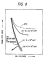
- Fig.8 is a graph showing the relationship between an on-voltage and a turn-off loss.
- the relationship is represented by using the life time of the carriers in the n- layer 8 as a parameter, with regard to each of the devices which have the total amount Q of the impurities in the p- layer 11.
- the improved trade-off relationship can be obtained, which is almost the same as the conventional SI thyristor.
- the device according to the present embodiment has a small on-voltage in the range of the wide turn-off loss. The reason why the trade-off is improved will be explained hereinafter.
- the device according to the present embodiment has the carrier distribution in which the carrier concentration in the neighborhood of the p- layer 11 in the n- layer 8 is larger than that in the neighborhood of of the p+ layer 7 in n- layer 8. It is, thereby, possible to reduce both the on-voltage and the turn-off loss.
- Such the distribution of carrier concentration can be obtained by suppressing the injection amount of holes from the p+ layer 7 in the side of the anode, using the characteristic in which the injection efficiency of electrons from the cathode is high and using an anode-emitter shorting structure.
- the life time of carrier is longer than that of Fig.7 or 10 ⁇ s, the carrier distribution becomes similar to that shown at (d) of Fig.7. Therefor, the trade-off relationship between the turn-off loss and the on-voltage is deteriorated more than the device with the characteristic (d). If the life time is shortened less than 10 ⁇ s in the GTO of a 4.5 kV class, the device can not be latched, thus can not operate normally. According to the present embodiment, it becomes possible to apply the shorter life time of carrier even in a high blocking voltage device as of 4.5 kV class.
- this film acts to suppress the surface recombination in the side wall of the groove 12 and prevent the deterioration of the injection efficiency of electrons due to the shorter life time of carrier.
- the injection of the electrons is also affected by thickness of the p- layer 11, it is desirable that the thickness of the p- layer 11 is less than 50 ⁇ m in case of Q ⁇ 1013cm ⁇ .
- the means for decresing the total amount Q is desirable.
- it may provide an area in which the life time of carriers is lessen by proton radiation or the formation of an n buffer layer. Further, it may set the concentration of the anode p+ layer 7 to less than 1018cm ⁇ . It may also use both of them.
- Figs.9A to 9J each is a schematic view of the step of a manufacturing process of the device or element.
- An n type Si substrate is prepared (Fig.9A)
- the p- layer 11 is formed by using thermal diffusion of p type impurities (Fig.9B)
- the p layer 19 in the periphery of the device is formed by thermal diffusion.
- the p+ layer 7 in the anode side and the n+ layer are formed (Fig.9D)
- the n+ layer in the cathode side is formed (Fig.9E).
- the groove 12 is formed by anisotrophic dry etching (Fig.9F).
- the anisotrophic dry etching is performed to the silicon oxide film, thus silicon oxide 14 is left in the side wall of the groove 12 (Fig.9G).
- the gate p+ layer 10 is formed on the bottom of the groove by using the diffusion of the p type impurities, and the silicide layer 15 is formed self-alignedly on the exposed part of the Si (Fig.9H).
- the resin layer 16 is formed for surface protection of the electrode and the device (Fig.9J).
- the device is completed after the life time control due to the irradiation of electron rays or ⁇ rays and a packaging process.
- a p layer 19 in the periphery of the device has the impurities higher than the p- layer 11. Therefore, if the layer is formed by the diffusion due to the same thermal processing, the p layer 19 is formed more deeply, the resultant pn junction has a convex portion. It is not desirable for the blocking voltage. It is possible to adjust the diffusion depth of both layers by diffusing in advance only the p- layer 11 and to make the pn junction 18 to be flat. Even if the impurities of which the diffusion is faster than that of the p layer 19 are used as the impurities of the p- layer 11, this purpose is attained.
- the p- layer 11 has been formed by ion-implanting borons (B) into the surface and diffusing thermally them.
- the desired p- layer 11 can be formed by adjusting the B dose amount. It may use Al (Alminium) or Ga (Gallium) as the impurities of the p- layer 11. Further, it may form a diffusion source by the deposition, etc. Because even if there is the dispersion in the condition of the diffusion layer, a high perfomance device can be made stably, it is possible to use a variety of methods for forming the p- layer.
- Figs.10A and 10B are a gragh and a table showing an example of the impurity distribution of a p- layer produced by using the manufacturing process shown in Figs.9A to 9J and conditions thereof, respectively.
- the p-layer 11 and the gate p+ layer 10 show the distribution of impurities along the Gauss distribution. Thereby, it is possible to heighten the gate blocking voltage.
- the gate blocking is 80 volts and in the remainder conditions, they are 100 volts to 180 volts.
- the impurity total amount Q' and Q'' and the dimension I2 shown at table 1 are also important quantity for the characteristics. The effect of the desirable numeral range of the total amount Q' and Q'' and the dimension I2 will be explained next.
- Numeral 22 of Fig.3E designates a horizontal surface of a part of the gate p+ layer 10 nearest to the n- layer 8, and 23 horizontal surface including the above horizontal surface.
- Numeral 24 designates an area p- layer 11 in a diretion of the n- layer 8 from the horizontal surface 23.
- the total amount of the impurities in this region converted into the amount per unit area of cross section, is called as the total amount Q' of the impurities in the n- layer side of the p- layer 11.
- Numeral 25 of Fig.3F designates a part of the gate p+ layer 10 nearest to the n- layer 8, and 26 a horizontal surface including the above horizontal surface.
- Numeral 27 designates an area of the p- layer 11 in a diretion of the n+ layer 9 from the horizontal surface 23. The total amount of the impurities in this region converted into the amount per unit area of cross section, is called as the total amount Q'' of the impurities in the n+ layer side of the p- layer 11.
- Figs.11A is a graph showing the relationship between the total amount Q' of impurities and the anode blocking voltage, in which the voltage between the gate and the cathode is 0 volt. if Q' ⁇ 1.2 x 10 11 cm ⁇ , the anode blocking voltage is heightened. In addition, the dependence of the blocking voltage on the width of a channel is lessened. Where, the deterioration of the blocking voltage which occurs in the Q' ⁇ 1.2 x 1011cm ⁇ is mild compared with that in the Q ⁇ 101cm ⁇ .
- Figs.11B is a graph showing the relationship between the total amount Q'' of impurities and the anode blocking voltage.
- the voltage between the gate and the cathode is - 100 V when an anode current is in a turn-off state.
- Figs.11C is a graph showing the relationship between the anode blocking voltage and the dimension I2 of a p+ layer, and that between the on-voltage and the dimension I2. If Q, Q' and Q'' are set to more than the predetermined value of the present invention and 1 ⁇ m ⁇ I2 ⁇ 3 ⁇ m, the anode blocking voltage is heightened and the on-voltage is suppressed to be low.
- Figs.12A to 12C are illustrations showing the mechanism of Fig.11A. They show the position where the distribution of the eqipotential line and the electric field is maximum when the anode voltage of the extent of 400 V is applied. Where, the circuit between the gate and the cathode is opened.
- Fig.12A shows the case in which the total amount Q' of impurities is smaller than the predetermined range of the present embodiment.
- the electric field is maximum at the curved portion of the bottom of the gate p+ layer 10. Therefore, the avalanche breakdown is liable to occur therein. When the anode voltage is heighten a little beyond this state, the electric field reach the limited value, the avalanche breakdown occurs, and it is difficult to prevent the higher anode voltage.
- the reason why the electric field is maximum is as follows.
- the total amount Q' is large compared with the case of Fig.12A, the invasion of the depletion from the pn junction 18 is lessened. Therefore, the imbalance of the distribution of the electric potential at the curved portion of the bottom of the gate p+ layer 10, that is, the curvature of the equipotential line is lessened. In addition, the amount of the space charges in the gate p+ layer is decreased. As compared with the case of Fig.12A, the maximum electric field is lessened and the avalanche breakdown voltage or the blocking voltage is heightened.
- Fig.12C shows the case that the total amount Q' of impurities is within the predetermined range, but it is relatively large.
- the maximum electric field at the curved portion of the bottom of the gate p+ layer 10 is further lessened.
- the maximum electric field is produced in the pn junction 18.
- the improvement of the blocking voltage is further confirmed.
- the width of the channel is enlarged, the invasion of the depletion layer into the p-layer 11 is increased. Therefore, the curvature of the equipotential line is emphasized, namely, the maximum electric field is heightened.
- the invasion of the depletion layer is lessened and the depencence of the maximum electric field on the width of the channel is extremely lessened.
- Figs.13A to 13C are illustrations showing the mechanism of Fig.11B. These figures show the distribution of the equipotential line and the position where the electric field is maximum when the anode voltage more than 3000 V is applied.
- the gate-cathode voltage is - 100 V.
- Fig.13A shows the case of the conventional SI thyristor which has not the p- layer 11. It becomes possible to produce the potential barrier in the channel and prevent the higher voltage by applying the inverse bias voltage between the gate and the cathode even in the conventional SI thyristor. Because there is not the p- layer 11, the anode voltage is prevented by the curved pn junction which comprises the gate p+ layer 10 and the n- layer 8.
- the equipotential line of the gate electric potential, -100 V and -80 V is curved along the gate p+ layer. Accordingly, the maximum strength of the electric field exists in the p+ layer 10.
- Fig.13B shows the case that the device has the p- layer 11, but the total amount Q'' is smaller than the predetermined value of the present embodiment.
- the equipotential line of the gate electric potential or -100 V are curved along the gate p+ layer 10 just like the case of Fig.13A.
- the depletion layer or the electric field which expands from the pn junction comprising the p- layer 11 and the n+ laye 9 by the gate inverse bias voltage invades largely into the p- layer 11 and reach the gate p+ layer 10.
- This depletion layer collides with another depletion layer from the pn junction 18.
- this phenominum is referred to as a reverse pinch effect. If the total amount Q'' Fig.13C is within the predetermined value of the present invention, all the equipotential lines cross the unit device.
- the curvature of the equipotential line is smaller, that is, the maximum electric field is lessened. Because the total amount Q'' of impurities is large in this case, the depletion layer due to the gate inverse bias does not reach the gate p+ layer 10, thus the reverse pinch effect is not occurred. Therefore, the electric field is moderated, thus the anode blocking voltage is heightened. If the channel width W is increased under the condition of Fig.13B, the invasion of the depletion layer into the p- layer 11 due to the gate inverse bias is increased. As a result, the curvature of the equipotential line becomes large, that is, the maximum electric field is strengthened. In the device according to the present embodiment shown in Fig.13C, the invasion of the depletion layer into the p- layer 11 due to the gate inverse bias is lessened, thus the dependence of the maximum electric field on the channel width is substantially diminished.
- the maximum concentration of impurities of the gate is set to higher than 1 x 1018cm ⁇ in order to decrease the gate resistance. It is not desirable to increase the maximum concentration of impurities of the gate p+ layer 10 from the point of view of the anode blocking voltage. Because the difference between the expansion of the gate p+ layer 10 and that of the p- layer 11 is large when the concentration of the gate p+ layer 10 is high, the electric potential line extremely curves and the amount of the space charge in the gate p+ layer 10 increases. By this effect, it is easy to generate a large electric field at the curved portion of the bottom of the gate p+ layer 10.
- the depth 12 In order to weaken the electric field, it is required to make the depth 12 from the bottom of the groove 12 of the gate p+ layer 10 deep. Thereby, because the expansion in the lateral direction of the impurity diffusion in the gate p+ layer 10, the curvature of radius of the edge portion of the gate p+ layer 10 can be made large. As a result, the electric field is moderated. However, if the depth I2 is too large, the on-voltage is unwillingly heightened. The reasons are as follows; (1) the distance in the vertical direction of the electric current passage is made longer, and (2) the area ratio of the current passage between the gate p+ layers 10 is lessened.
- the depth of the gate p+ layer 10, 1 ⁇ m ⁇ I2 ⁇ 3 ⁇ m, of the present embodiment is smaller than that of the conventional SI thyristor. Therefore, there is an advantage in a point of the low on-voltage of a device.
- the maximum concentration of impurities of the gate p+ layer 10 is increased to higher than 1 x 1018cm ⁇ 3 in the present embodiment. If the concentration of impurities of the gate p+ layer 10 is high, it is possible to decrease the contact resistance between the gate p+ layer 10 and the gate wiring layer 15 and decrease the parasitic resistance of the gate circuit. As a result, it becomes possible to allow confirmly and in a high speed a current to turn off. If the maximum concentration of impurities of the gate p+ layer 10 is heighten to more than 1019cm ⁇ 3, it is possible to form the ohmic-contact even by using an aluminium which a metal silicide or silicon is added, as the gate wiring layer 15.
- the gate wiring layer 15 can be fined in this case.
- the problem that occurs the fault of the blocking voltage also can be solved, in which the fault is made by a spike pulse when the ohmic-electrode is formed. If the alminium without additives is used as the gate wiring layer 15, there is an advantage that can lessen extremely the resistance of the gate wiring layer 15 itself. It is also effective to adopt the structure in which the alminium that the metal silicide layer or silicon is added between the gate p+ layer and the alminium layer without additives.
- the total amount Q of impurities is set to the smaller value compared with the p base layer 30 of a GTO in order to decrease the loss.
- the depletion layer is relatively easy to invade into the p- layer 11.
- the anode voltage is prevented by the plane pn junction 18, the equipotential line is curved and a large electric field is generated, which occurs an avalanche breakdown. Thereby, the blocking voltage is determined.
- Fig.2A the structure of a sectional surface of the peripheral region of the device will be explained.
- the side surface of the device is processed by a beveling machining.
- a p+ layer 101 and a silicide layer 151 are formed on the peripheral portion of the device in the forming process of the p+ layer 10 and the silicide layer 15. Because the concentration of the p- layer 11 is low, a channel is formed on the surface of the p- layer due to the MOS effect when only the p- layer 11 is formed on the peripheral portion.
- the p+ layer 101 has the function of preventing the formation of such the harmful channel.
- the formation of the channel is prevented confirmly by providing a p layer 19 which has the impurity concentration higher than the p- layer 11. Because the p layer 19 has the function of lessening the effect of charges outside of the device on the potential distribution inside of the device, it also can solve the problem that the anode blocking voltage deteriorates after a long time periods of use.
- the depth of the groove provided with the gate electrode 6 is different from that inside of the segment. This is because the etching rate is different according to the depth of the grooves when they are formed by using the anisotropic dry etching method.
- the difference of the depth of the grooves becomes large when the width of the grooves inside the segment is fined in order to increase the area ratio of the n+ layer 9 for the low on-voltage.
- the difference of the depth of the grooves brings that of the position in a vertical direction of the p+ layer 11. This means that the effective width of the channel becomes extremely long.
- the unit device in the outermost part of the segment limits an anode voltage to a low one.
- the effective Q' is important, the quantity converted the total amount of impurities of the region in the n- layer 8 side from the horizontal surface including the bottom of the gate p+ layer 10 of the groove with the gate electrode 6 in the low concentration layer, the p- layer 11, into the amount per unit area of cross section. It is advantageous for the blocking voltage to allow the effective Q' to be as large as possible, under the condition of Q ⁇ 1014cm ⁇ ; preferably Q' ⁇ 1.2 x 1011cm ⁇ .
- the total amount Q'' of impurities in the cathode 9 side of the low concentration layer, the p- layer 11, may be desirable to Q'' ⁇ 8 x 1011cm ⁇ . As decribed above, it is possible to fine the width of the groove inside the segment into 10 ⁇ m. This contributes to the low on-voltage.
- the anode blocking voltage is lessen by the effect of the convex shape of the bottom of the p layer 19. It is desirable to select the depth of the p- layer 11 and the p layer 19 so as that both depth is not diffent from each other, or to form the pn junction in a plane by making the p- layer 11 deeper than the p layer 19 as shown in Fig.2A.
- Fig.14 is a graph showing the impurity distribution in a modification of the first embodiment. While to form the groove and then to form the gate p+ layer on the bottom thereof is the same as the previous example, the p- layer 11 is formed by using the epitaxial growth in this example. The control of the total amount of impurities is easy, and the high gate bloking voltage is obtained easily by increasing the total amounts Q, Q' and suppressing the maximum impurity concentration.
- Figs.15A to 15C are views each showing a plane pattern of a cathode n+ layer.
- the portion marked by n+ designates the n+ layer, and other portions designate the groove 12.
- the segment is constructed by the combination of the n+ layer 9.
- a plurality of segments is arranged in a radial direction of a disk-like device or element in a way similar to the conventional GTO.
- I5 is in the range of several tens of ⁇ m to 300 ⁇ m
- I6 is in the range of 1 mm to 4 mm.
- one plane pattern is rectangular, in which it is possible to increase the area ratio of the n+ layer 9 and easily to obtain the high blocking voltage.
- Fig.15B one plane pattern is square.
- the p+ layer 10 is in a higher density state compared with the example of Fig.15A, it is easy to obtain the high blocking voltage and it is possible to realize a device with higher speed operation and a device with large turn-off capability.
- the making of a photo mask also is comparatively easy.
- Fig.15C one plane pattern is circular. Because the p+ layer 10 has the highest density compared with the examples of Figs.15A and 15B, it is easy to obtain the highest blocking voltage. Because in either cases, the n+ width 13 is set to the range of several ⁇ m to several tens of ⁇ m and the p+ layer 10 of the bottom of the groove 12 is in a high density state, the extraction efficiency of holes from the gate when the device is turned off is superior. Therefore, it is possible to obtain a device with high speed operation and a device with large turn-off capability. It is desirable to select the width I4 of the groove to the range of several ⁇ m to aeveral tens of ⁇ m.
- Figs.16A and 16B are views showing a modification of the first embodiment.
- the anode p+ layer 7 (hereinafter, referred to as an anode p layer) is used instead of the anode-emitter shorting structure.
- the injection of the holes from anode p layer 7 to n- layer 8 is performed by lessening the impurity concentration of the anode p layer to less than 1018cm ⁇ 3.
- the carrier concentration in the neighborhood of the p- layer 11 in the n- layer 8 becomes larger than that in the neiborhood of the anode p layer 7 in n- layer 8.
- the impurity concentration of the anode p layer 7 is preferably in the range of 1016cm ⁇ 3 to 1017cm ⁇ 3, The effect of the improvement of the trade-off between the on-voltage and the turn-off loss. Further, the turn-on is.fast compared with the device having the anode-emitter shorting structure. This is because the injection of holes is started from all of the regions of the anode p layer 7 when turned on.
- Figs.17A and 17B are views showing an example in which a silicide layer is inserted between an anode p layer and an aluminium layer of an anode electrode in Fig.16.
- the silicide layer 28 forms a barrier for stopping the diffusion of alminium from the alminium layer 4, and prevent the diffusion of alminium from the anode electrode aluminium layer 4 into the anode p layer 7. It is, therefore, easy to form the anode p layer with lower concentration.
- the alminium with silicon added may be used as a material of the anode electrode 4, instead of the silicide layer 28.
- Figs.18A to 18C and Figs.19A to 19C are views showing an device of a buried gate type.
- the device of this type will be called as a second embodiment hereinafter.
- the gate p layer is the p+ layer with high impurity concentration. Because it has the burried gate p+ layer 10, the definition of the region of the gate p+ layer 10 is different from that in the first embodiment.
- numeral 29 designates the position where the impurity concentration in the gate p+ layer 10 is maximum. In this case, it is extremely narrow, so that it may be regarded as a point in fact.
- Numeral 20 designates the region where the impurity concentration is more than 1/10 one of the maximum concentration.
- the total amount Q, Q', Q'' and the distance I2 is set to the same values as the first embodiment.
- the p- layer with low concentration is comprised of an epitaxial growth layer 111 and a diffusion layer 112 formed before the epitaxial growth, the total amounts Q, Q', Q'' can be adjusted easily.
- Figs.20A and 20B are a gragh and a table showing an example of the impurity distribution of a p- layer and conditions thereof, respectively.
- the total amount Q' and Q'' can be adjusted independly, namely, the Q' can be adjusted by the amount of the impurities of the diffusion layer 112, and the Q'' by the amount of the impurities of the epitaxial growth layer 111. Accordingly, compared with the case of Fig.10, it is easy to obtain the high gate blocking voltage and the high anode blocking voltage at the same time.
- the conventional SI thyristor of the burried gate type has large and harmful effects (the increasement of turn-on time and an on-voltage, etc.) of auto-doping in which the impurities of the p+ layer 10 is diffused outside Si and re-diffused into the channel region. Because it is possible to maintain the high anode blocking voltage and to make the width of a channel long by providing the p- layer, such the harmful effects of an out-diffusion is lessen, thus it becomes possible to produce a large device with high efficiency.
- Figs.21A to 21F shows other embodiments of the present invention, and is an enlarged view in the neighborhood of the cathode 5 of the unit device.
- the cathode n+ layer and the gate p+ layer 10 is isolated from the n- layer 8 by the p- layer 11 in these devices. Further, the total amount of impurities in each portion of the p- layer defined in a way similar to that of Fig.3 is set to the value defined in the above embodiment.
- Fig.21A shows the structure in which a slightly low concentration layer 113 is provided along the groove 12.
- the low concentration layer 113 moderates the electric field in the curved portion of the bottom of the gate p+ layer, and sometimes forms a current path. It is not required to make the gate p+ layer 10 thick, because of the moderating function of the electric field. It is provided just for the ohmic-contact with the gate wiring layer 15. As seen from the above, this device is effective in a view point of a lower on-voltage. Futhermore, the low concentration layer 113 acts to avoid the harmful effect due to the channel formed unwillingly on the surface of the side wall of the groove 12.
- Fig.21B shows the structure in which a slightly low concentration layer 115 is provided in the neighborhood of the bottom of the groove 12.
- the low concentration layer 115 acts in a way similar to that of Fig.21B. It is advantageous for making the on-voltage low, because of the narrow low concentration layer.
- Fig.21C shows the structure in which the p- layer 11 is diffused. It is possible to obtain a high blocking voltage, by making the thickness of the p- layer 11 thin and by making the concentration comparatively high. Because the p- layer 11 is thin, it is advantageous to make an on-voltage low.
- An n- layer 81 between the p- layer 11 and the n+ layer 9 is a portion of the n- substrate with low impurity concentration. Therefore, it is advantageous to make an on-voltage low as compared with the device as described later, in which the n- layer 81 is formed by the epitaxial growth. Because most of the depletion layer expand toward the n- layer 8, it is hard to arise the drop of the blocking voltage due to the reverse pinch effect.
- Fig.21D shows a burried gate structure, in which the n- layer is provided between the p- layer 11 and the n+ layer 9.
- This embodiment also can make effectively a blocking voltage high and make an on-voltage low.
- an pn junction can be formed in a plane, the high anode blocking voltage and the high gate blocking voltage can be obtained.
- Fig.21E shows a burried gate structure, in which a slightly low concentration layer 115 is provided along the burried gate layer 10. This structure is also effective to make an on-voltage low by the same reason as one of Fig.21B.
- Fig.21F shows a planar diffused gate type structure. According to this embodiment, it is easy to produce and it has a good yield. It is advantageous to make an on-voltage low in a device with a thin p- layer (11).
- Fig.22 is a circuit diagram showing an example of a power converter for motor driving circuit, using the semiconductor devices (SW11, SW12, SW21, SW22, SW31, SW33) of the present embodiment 1 as switching elements
- Fig.23A is a schematic view showing a conventional recessed gate type SI thyristor.
- Fig.23B is a schematic view showing a conventional GTO.
- the inverter unit for one phase is constructed by connecting two switching elements (ex. SW11 and SW12) in series.
- a free wheel diode FD is connected in inverse parallel to each of the switching elements.
- a so-called anubber circuit S is connected in parallel to each of the switching elements, for protecting the switching element from the rapid rise-up of the voltage.
- This snubber circuit is constructed by connecting in series a parallel circuit of a diode SD ans a resistor SR to a capacitor SC.
- the serial connection point of two switching elements in each phase is connected to each of an alternating current terminals (T3, T4, T5).
- a three-phase induction motor is connected to the AC terminals.
- the anodes of the switching elements of the upper arm side are connected in common and are connected to a high voltage side of a DC voltage source at a DC terminal T1.
- the cathodes of the switching elements of the lower arm side are connected in common and are connected to a low voltage side of a DC voltage source at a DC terminal T2.
- the three-phase induction motor is driven by converting a DC to an AC due to switching operation.
- a gate circuit for control the switching operation is connected between a gate and a cathode of each switching element of the upper and the lower arm sides.
- the switching elements has the characteristics of a high blocking vlotage and a low loss, it is possible to produce the inverter equipment with a high blocking voltage and a high efficiency. Further, because a high performance device can be produce effectively, it is possible to realize a high performance system at a low cost. It should be noted that any semiconductor devices according to the present invention can be used in a power converter of the present invention and similar effects are obtained in such a modification.
Landscapes
- Thyristors (AREA)
- Electrodes Of Semiconductors (AREA)
Applications Claiming Priority (2)
| Application Number | Priority Date | Filing Date | Title |
|---|---|---|---|
| JP148972/94 | 1994-06-30 | ||
| JP14897294A JP3214236B2 (ja) | 1993-06-30 | 1994-06-30 | 半導体装置及び電力変換装置 |
Publications (2)
| Publication Number | Publication Date |
|---|---|
| EP0696066A2 true EP0696066A2 (de) | 1996-02-07 |
| EP0696066A3 EP0696066A3 (de) | 1998-06-24 |
Family
ID=15464799
Family Applications (1)
| Application Number | Title | Priority Date | Filing Date |
|---|---|---|---|
| EP95304623A Withdrawn EP0696066A3 (de) | 1994-06-30 | 1995-06-30 | Schaltungs-Halbleiterbauteil und Leistungswandler |
Country Status (2)
| Country | Link |
|---|---|
| US (1) | US5831293A (de) |
| EP (1) | EP0696066A3 (de) |
Cited By (1)
| Publication number | Priority date | Publication date | Assignee | Title |
|---|---|---|---|---|
| EP1156532A3 (de) * | 2000-05-15 | 2003-11-26 | Kabushiki Kaisha Toshiba | Elektroden-Kontaktzone einer Halbleiteranordnung |
Families Citing this family (2)
| Publication number | Priority date | Publication date | Assignee | Title |
|---|---|---|---|---|
| WO2015154908A1 (en) * | 2014-04-10 | 2015-10-15 | Abb Technology Ag | Turn-off power semiconductor device with improved centering and fixing of a gate ring, and method for manufacturing the same |
| DE102018215827B3 (de) * | 2018-09-18 | 2019-09-19 | Siemens Aktiengesellschaft | Schaltvorrichtung zum Auftrennen eines Strompfads |
Family Cites Families (9)
| Publication number | Priority date | Publication date | Assignee | Title |
|---|---|---|---|---|
| US4198645A (en) * | 1976-01-27 | 1980-04-15 | Semiconductor Research Foundation | Semiconductor controlled rectifier having gate grid dividing surrounding zone into two different impurity concentration sections |
| JPS5432982A (en) * | 1977-08-18 | 1979-03-10 | Mitsubishi Electric Corp | Manufacture of gate turn off thyristor |
| JPS5959070A (ja) * | 1982-09-29 | 1984-04-04 | Hitachi Ltd | ゲ−ト・タ−ンオフ・サイリスタを用いた電力変換装置 |
| EP0121068B1 (de) * | 1983-03-31 | 1988-01-13 | BBC Brown Boveri AG | Leistungshalbleiterbauelement und Verfahren zu dessen Herstellung |
| EP0178387B1 (de) * | 1984-10-19 | 1992-10-07 | BBC Brown Boveri AG | Abschaltbares Leistungshalbleiterbauelement |
| US4752818A (en) * | 1985-09-28 | 1988-06-21 | Kabushiki Kaisha Toyota Chuo Kenkyusho | Semiconductor device with multiple recombination center layers |
| CH670528A5 (de) * | 1986-03-20 | 1989-06-15 | Bbc Brown Boveri & Cie | |
| JP2960506B2 (ja) * | 1990-09-19 | 1999-10-06 | 株式会社日立製作所 | ターンオフ形半導体素子 |
| DE69223738T2 (de) * | 1991-10-31 | 1998-05-14 | Toshiba Kawasaki Kk | MOS-Gate-kontrollierter Thyristor |
-
1995
- 1995-06-30 EP EP95304623A patent/EP0696066A3/de not_active Withdrawn
-
1996
- 1996-09-06 US US08/709,451 patent/US5831293A/en not_active Expired - Fee Related
Non-Patent Citations (1)
| Title |
|---|
| None |
Cited By (2)
| Publication number | Priority date | Publication date | Assignee | Title |
|---|---|---|---|---|
| EP1156532A3 (de) * | 2000-05-15 | 2003-11-26 | Kabushiki Kaisha Toshiba | Elektroden-Kontaktzone einer Halbleiteranordnung |
| US7271040B2 (en) | 2000-05-15 | 2007-09-18 | Kabushiki Kaisha Toshiba | Electrode contact section of semiconductor device |
Also Published As
| Publication number | Publication date |
|---|---|
| US5831293A (en) | 1998-11-03 |
| EP0696066A3 (de) | 1998-06-24 |
Similar Documents
| Publication | Publication Date | Title |
|---|---|---|
| US6696705B1 (en) | Power semiconductor component having a mesa edge termination | |
| JP7724284B2 (ja) | 信頼性及び導通が向上したトレンチ型パワー・デバイス | |
| US4972239A (en) | Conductivity modulated MOSFET | |
| EP0430237A1 (de) | Bipolar-Bauelement, in welchem die Ladungsträgerlebensdauer kontrolliert wird | |
| JPH05183114A (ja) | 半導体装置 | |
| JP2000323488A (ja) | ダイオードおよびその製造方法 | |
| EP3948956B1 (de) | Segmentierte leistungsdiodenstruktur mit verbesserter reverse recovery | |
| CA2013349C (en) | Fet, igbt and mct structures to enhance operating characteristics | |
| EP0024657B1 (de) | Thyristor mit ununterbrochenem Emitternebenschluss | |
| US6734520B2 (en) | Semiconductor component and method of producing it | |
| US5387805A (en) | Field controlled thyristor | |
| US4517582A (en) | Asymmetrical thyristor with highly doped anode base layer region for optimized blocking and forward voltages | |
| US5874751A (en) | Insulated gate thyristor | |
| US5072312A (en) | Thyristor with high positive and negative blocking capability | |
| GB2612636A (en) | Semiconductor device | |
| KR100476849B1 (ko) | 전계 형성 영역을 포함한 반도체 스위칭 소자 | |
| Kekura et al. | 8000 V 1000 A gate turn-off thyristor with low on-state voltage and low switching loss | |
| JP4001249B2 (ja) | 高ブロッキング電圧用ゲート・ターンオフ・サイリスタ | |
| US5831293A (en) | Semiconductor thyristor switching device and power converter using same | |
| EP1713128B1 (de) | IGBT und diesen verwendende elektrische Stromwandlungsvorrichtung | |
| US6252257B1 (en) | Isolating wall between power components | |
| EP0862220A1 (de) | Halbleiter-Schaltelement und Leistungsumwandler unter Benutzung desselben und diesbezügliches Verfahren zum Betreiben desselben | |
| US11069769B2 (en) | Semiconductor device | |
| JP3214236B2 (ja) | 半導体装置及び電力変換装置 | |
| US6559515B1 (en) | Insulating wall between power components |
Legal Events
| Date | Code | Title | Description |
|---|---|---|---|
| PUAI | Public reference made under article 153(3) epc to a published international application that has entered the european phase |
Free format text: ORIGINAL CODE: 0009012 |
|
| 17P | Request for examination filed |
Effective date: 19950719 |
|
| AK | Designated contracting states |
Kind code of ref document: A2 Designated state(s): DE GB |
|
| PUAL | Search report despatched |
Free format text: ORIGINAL CODE: 0009013 |
|
| AK | Designated contracting states |
Kind code of ref document: A3 Designated state(s): DE GB |
|
| 17Q | First examination report despatched |
Effective date: 20020327 |
|
| STAA | Information on the status of an ep patent application or granted ep patent |
Free format text: STATUS: THE APPLICATION IS DEEMED TO BE WITHDRAWN |
|
| 18D | Application deemed to be withdrawn |
Effective date: 20020409 |