EP0696064A2 - Monolithisch integrierte VLSI, optoelektronische Schaltkreise und Herstellungsverfahren für diese - Google Patents
Monolithisch integrierte VLSI, optoelektronische Schaltkreise und Herstellungsverfahren für diese Download PDFInfo
- Publication number
- EP0696064A2 EP0696064A2 EP95305041A EP95305041A EP0696064A2 EP 0696064 A2 EP0696064 A2 EP 0696064A2 EP 95305041 A EP95305041 A EP 95305041A EP 95305041 A EP95305041 A EP 95305041A EP 0696064 A2 EP0696064 A2 EP 0696064A2
- Authority
- EP
- European Patent Office
- Prior art keywords
- compound semiconductor
- semiconductor surface
- devices
- optical devices
- optical
- Prior art date
- Legal status (The legal status is an assumption and is not a legal conclusion. Google has not performed a legal analysis and makes no representation as to the accuracy of the status listed.)
- Withdrawn
Links
- 230000005693 optoelectronics Effects 0.000 title claims abstract description 11
- 238000004519 manufacturing process Methods 0.000 title description 2
- 230000003287 optical effect Effects 0.000 claims abstract description 50
- 239000004065 semiconductor Substances 0.000 claims abstract description 37
- 150000001875 compounds Chemical class 0.000 claims abstract description 35
- 239000012535 impurity Substances 0.000 claims abstract description 7
- 229910001218 Gallium arsenide Inorganic materials 0.000 claims description 22
- 238000000034 method Methods 0.000 claims description 22
- 230000005669 field effect Effects 0.000 claims description 6
- 238000005162 X-ray Laue diffraction Methods 0.000 claims description 5
- 239000000356 contaminant Substances 0.000 claims description 4
- 238000000171 gas-source molecular beam epitaxy Methods 0.000 claims description 4
- 230000003213 activating effect Effects 0.000 claims description 3
- 238000012545 processing Methods 0.000 claims description 3
- YZCKVEUIGOORGS-UHFFFAOYSA-N Hydrogen atom Chemical compound [H] YZCKVEUIGOORGS-UHFFFAOYSA-N 0.000 claims description 2
- 238000002003 electron diffraction Methods 0.000 claims description 2
- 239000007789 gas Substances 0.000 claims description 2
- 239000010410 layer Substances 0.000 description 16
- 238000003795 desorption Methods 0.000 description 14
- 238000001451 molecular beam epitaxy Methods 0.000 description 7
- 230000015572 biosynthetic process Effects 0.000 description 5
- 230000010354 integration Effects 0.000 description 5
- 230000001133 acceleration Effects 0.000 description 4
- 239000002344 surface layer Substances 0.000 description 4
- 229910000980 Aluminium gallium arsenide Inorganic materials 0.000 description 3
- 230000015556 catabolic process Effects 0.000 description 3
- 239000000463 material Substances 0.000 description 3
- 238000001228 spectrum Methods 0.000 description 3
- 230000007704 transition Effects 0.000 description 3
- UFHFLCQGNIYNRP-UHFFFAOYSA-N Hydrogen Chemical compound [H][H] UFHFLCQGNIYNRP-UHFFFAOYSA-N 0.000 description 2
- 239000004642 Polyimide Substances 0.000 description 2
- 238000000137 annealing Methods 0.000 description 2
- 238000010276 construction Methods 0.000 description 2
- 238000006731 degradation reaction Methods 0.000 description 2
- 230000005284 excitation Effects 0.000 description 2
- 239000001257 hydrogen Substances 0.000 description 2
- 229910052739 hydrogen Inorganic materials 0.000 description 2
- 238000011065 in-situ storage Methods 0.000 description 2
- 238000001465 metallisation Methods 0.000 description 2
- 229920001721 polyimide Polymers 0.000 description 2
- 238000002128 reflection high energy electron diffraction Methods 0.000 description 2
- 239000000758 substrate Substances 0.000 description 2
- 240000001492 Carallia brachiata Species 0.000 description 1
- OKTJSMMVPCPJKN-UHFFFAOYSA-N Carbon Chemical compound [C] OKTJSMMVPCPJKN-UHFFFAOYSA-N 0.000 description 1
- -1 GaAs Chemical class 0.000 description 1
- XUIMIQQOPSSXEZ-UHFFFAOYSA-N Silicon Chemical compound [Si] XUIMIQQOPSSXEZ-UHFFFAOYSA-N 0.000 description 1
- PNEYBMLMFCGWSK-UHFFFAOYSA-N aluminium oxide Inorganic materials [O-2].[O-2].[O-2].[Al+3].[Al+3] PNEYBMLMFCGWSK-UHFFFAOYSA-N 0.000 description 1
- 150000001450 anions Chemical class 0.000 description 1
- 238000003491 array Methods 0.000 description 1
- QVGXLLKOCUKJST-UHFFFAOYSA-N atomic oxygen Chemical compound [O] QVGXLLKOCUKJST-UHFFFAOYSA-N 0.000 description 1
- 229910052799 carbon Inorganic materials 0.000 description 1
- 239000000969 carrier Substances 0.000 description 1
- 150000001768 cations Chemical class 0.000 description 1
- 230000003749 cleanliness Effects 0.000 description 1
- 238000004891 communication Methods 0.000 description 1
- 238000007796 conventional method Methods 0.000 description 1
- 229910052593 corundum Inorganic materials 0.000 description 1
- 230000001419 dependent effect Effects 0.000 description 1
- 230000006866 deterioration Effects 0.000 description 1
- 239000003989 dielectric material Substances 0.000 description 1
- 239000002019 doping agent Substances 0.000 description 1
- 125000004435 hydrogen atom Chemical group [H]* 0.000 description 1
- 238000002513 implantation Methods 0.000 description 1
- 230000010365 information processing Effects 0.000 description 1
- 238000011835 investigation Methods 0.000 description 1
- 150000002500 ions Chemical class 0.000 description 1
- 239000002184 metal Substances 0.000 description 1
- 239000001301 oxygen Substances 0.000 description 1
- 229910052760 oxygen Inorganic materials 0.000 description 1
- 230000006798 recombination Effects 0.000 description 1
- 238000005215 recombination Methods 0.000 description 1
- 238000000682 scanning probe acoustic microscopy Methods 0.000 description 1
- 229910052710 silicon Inorganic materials 0.000 description 1
- 239000010703 silicon Substances 0.000 description 1
- 238000006467 substitution reaction Methods 0.000 description 1
- 230000003746 surface roughness Effects 0.000 description 1
- 238000003631 wet chemical etching Methods 0.000 description 1
- 229910001845 yogo sapphire Inorganic materials 0.000 description 1
Images

Classifications
-
- H—ELECTRICITY
- H10—SEMICONDUCTOR DEVICES; ELECTRIC SOLID-STATE DEVICES NOT OTHERWISE PROVIDED FOR
- H10H—INORGANIC LIGHT-EMITTING SEMICONDUCTOR DEVICES HAVING POTENTIAL BARRIERS
- H10H29/00—Integrated devices, or assemblies of multiple devices, comprising at least one light-emitting semiconductor element covered by group H10H20/00
- H10H29/10—Integrated devices comprising at least one light-emitting semiconductor component covered by group H10H20/00
-
- H—ELECTRICITY
- H10—SEMICONDUCTOR DEVICES; ELECTRIC SOLID-STATE DEVICES NOT OTHERWISE PROVIDED FOR
- H10F—INORGANIC SEMICONDUCTOR DEVICES SENSITIVE TO INFRARED RADIATION, LIGHT, ELECTROMAGNETIC RADIATION OF SHORTER WAVELENGTH OR CORPUSCULAR RADIATION
- H10F39/00—Integrated devices, or assemblies of multiple devices, comprising at least one element covered by group H10F30/00, e.g. radiation detectors comprising photodiode arrays
- H10F39/10—Integrated devices
- H10F39/103—Integrated devices the at least one element covered by H10F30/00 having potential barriers, e.g. integrated devices comprising photodiodes or phototransistors
-
- Y—GENERAL TAGGING OF NEW TECHNOLOGICAL DEVELOPMENTS; GENERAL TAGGING OF CROSS-SECTIONAL TECHNOLOGIES SPANNING OVER SEVERAL SECTIONS OF THE IPC; TECHNICAL SUBJECTS COVERED BY FORMER USPC CROSS-REFERENCE ART COLLECTIONS [XRACs] AND DIGESTS
- Y10—TECHNICAL SUBJECTS COVERED BY FORMER USPC
- Y10S—TECHNICAL SUBJECTS COVERED BY FORMER USPC CROSS-REFERENCE ART COLLECTIONS [XRACs] AND DIGESTS
- Y10S438/00—Semiconductor device manufacturing: process
- Y10S438/974—Substrate surface preparation
Definitions
- the present invention relates generally to monolithically integrated circuit devices and, more particularly, to metallized VLSI circuits having monolithically integrated optical interconnects formed thereon and to a process for fabricating the same.
- Surface normal modulating devices capable of high speed, optical information processing within massively parallel architectures are currently sought for use in a wide variety of communication systems. Such integration would be particularly advantageous in so-called smart pixels applications, where optical interconnects may be clocked at speeds beyond several Gbits/second.
- Surface normal modulating devices such as Multiple Quantum Well modulators (MQW's), for example, may be fabricated into large arrays capable of addressing electronic chips in systems handling 10,000 or more input/output optical beams. It is expected that the use of inter-chip optical interconnects within a high density digital processor operating above a few GHz will reduce skew in clock signal distribution as well as timing errors.
- MQW's Multiple Quantum Well modulators
- Shennoy et al. have reported the integration of Light Emitting Diodes (LEDs) on GaAs with completely metallized VLSI FETs. OSA Proceedings, p. 9433 (1993, San Diego).
- the fabrication technique disclosed by Shennoy et al employs an MBE (Molecular Beam Epitaxy) regrowth of the LEDs on a fully metallized GaAs IC, as supplied by Vitesse Semiconductor. Only a few of the FETs, however, are expected to survive the MBE regrowth, which requires an annealing temperature in excess of 530°C.
- modulator integration requires that a high density of VLSI FETs survive the MBE regrowth -- as many as 105/chip may be required -- the Shennoy et al. technique cannot be successfully employed.
- optical devices are grown on a compound semiconductor surface of a VLSI circuit having pre-existing electronic devices formed thereon to obtain monolithically integrated optoelectronic circuits.
- a wide variety of novel structures which could not be achieved with conventional thermal desorption and epitaxial growth techniques, may now be fabricated.
- the material comprising the compound semiconductor surface will, of course, depend upon the type and desired performance characteristics of the electrical and optical devices to be formed thereon and interconnected.
- the compound semiconductor surface may be selected from the group consisting of Group III-V compounds, such as GaAs, AlGaAs, and so on.
- the prefabricated electronic devices are field effect transistors and the optical devices are optical modulators.
- monolithically integrated VLSI circuits employing diverse combinations of electronic and optical devices may also be fabricated using the teachings of the present invention.
- other types of optical devices such as lasers and photodetectors, may also be grown on the compound semiconductor surface of a VLSI circuit.
- a process for fabricating VLSI optoelectronic circuits comprises the steps of removing surface contaminants from a compound semiconductor surface having a plurality of metallized electronic devices distributed over a portion thereof, and growing a plurality of optical devices on the compound semiconductor surface at a temperature below 500°C.
- the removing step comprises thermally activating the compound semiconductor surface while directing an atomic gas plasma at the surface.
- the plasma is hydrogen plasma, which may be directed at the compound semiconductor surface with an electron cyclotron resonance source.
- the compound semiconductor surface is preferably kept at or below 430°C during the removal step.
- the compound semiconductor surface is also preferably kept at or below 430°C while the optical devices are being grown thereon.
- optical devices as for example multiple quantum well optical modulators, may be formed by gas source molecular beam epitaxy even where the preferred 430°C temperature limit is observed.
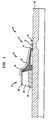
- each smart pixel 10 comprises a field effect transistor (FET) 12 having a source electrode 14, a gate electrode 16, and a drain electrode 18.
- FET field effect transistor
- the FETs are defined on a compound semiconductor surface layer 20 doped to a predetermined conductivity type.
- the conductivity type and the dopant concentration, as well as the specific material comprising the surface layer 20 will depend upon the desired electrical and optical properties of the devices to be fabricated thereon.
- surface layer 20 may be formed of any desired combination of Group III-V semiconductor materials which has the appropriate or desired electrical properties and upon which the desired optical and electronic devices may be grown or otherwise formed.
- layer 20 comprises an n-type implantation layer of GaAs on a (001) GaAs insulating substrate.
- metallized VLSI chips having a dense array of electronic devices such as FETs fabricated on such a compound semiconductor surface are commercially available.
- a suitable chip having an array of over 10,000 FETs provided thereon, for example, is available from Vitesse Semiconductor of Camarillo, California.
- Vitesse Semiconductor of Camarillo, California it has not been feasible to fabricate monolithically integrated smart pixel elements on such commercially available structures.
- each smart pixel 10 of optoelectronic circuit 11 is formed by growing an optical device 22 on surface layer 20 and providing an electrical connection to the drain electrode 18 of an associated FET 12.
- the optical device 22 is a multiple quantum well optical modulator having a Distributed Bragg Reflection (DBR) layer 24, a multiple quantum well layer 26, and a transparent cap layer 28.
- DBR Distributed Bragg Reflection
- the general construction and operating characteristics of such modulators are well known to those skilled in the art and for this reason, a detailed description of the same is deemed unnecessary and has been omitted from this description.
- a device chip, such as chip 11, having metallized devices already formed thereon is first placed within an ECR plasma chamber (not shown). It is believed that those skilled in the art are familiar with the construction of ECR processing systems which may be utilized for ECR-assisted desorption in accordance with the present invention. For examples of systems which may be so utilized, reference may for example be had to several papers published by the Journal of Applied Physics including one paper by C. Wood (No. 51,2074, 1980), and several by K.D. Choquette et al. (Nos. 73,2035 and 62,2658, 1993) .
- an Al2O3 cup is employed in the microwave cavity of the ECR source to avoid auto doping of the GaAs with Si (as would be the case if a SiO cup were used).
- the ECR source is also preferably equipped with an acceleration grid to enhance the kinetic energy of protons striking the compound semiconductor surface.
- the time required for ECR-assisted desorption depends upon the acceleration voltage and the temperature of the compound semiconductor surface. With GaAs, a voltage of 60V, a surface temperature of 350°C, and a desorption time of 10 minutes have been found to produce satisfactory results.
- optical devices such as an MQW optical modulator are grown thereon.
- a DBR layer 24 (FIG. 1) consisting of alternating layers (not shown) of low index AlAs and high index AlGaAs 50 is grown.
- MQW layer 26 consisting of superlattices of 50 periods of .095 micron GaAs CW and .035 micron Al 0.3 Ga 0.7 As, for a total thickness of approximately 2 microns, is grown on the surface of DBR layer 24 by gas source MBE at 430°C in a pin geometry. Finally, a transparent 0.5 micron cap layer 28 of p-type AlGaAs is grown on the surface of MQW 28.
- drain electrode 18 To facilitate subsequent electrical interconnection of drain electrode 18 with cap layer 28 by metallization, a layer 30 of polyimide or other dielectric material is deposited therebetween to provide an even, gradually tapered path.
- a metal overlay 32 for interconnecting drain electrode 18 and cap layer 28 is patterned and deposited over polyimide layer 30, thereby resulting in the structure depicted in FIG. 1.
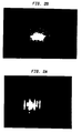
- FIGS. 2A and 2B illustrate the results obtained from two ECR desorbed GaAs surfaces obtained respectively with 2 and 10 minute exposure to hydrogen protons under the above-described conditions.
- the two surfaces corresponded to the C 4x2 and C 4x4, which are the anion and cation rich surfaces of GaAs.
- Both surfaces exhibited remarkable diffraction structure as evidenced by the appearance of spots intersecting the 0th order Laue zone. Smaller intensity was diffracted into elongated streaks, thus indicating low surface disorder.
- the surfaces differed from the spotty, uneven surface character which often accompanies thermal desorption.
- the Ga-rich surface showed the highest degree of surface ordering as indicated by the appearance of five distinct Laue zones. In situ auger spectroscopy carried out on these surfaces showed no evidence of impurities after the desorption process.
- superlattice emission consists of light and heavy hole exciton (lh and hh) with a splitting of 11 meV.
- the FWHM of the heavy transition was 4.3 meV.
- the spatially indirect transition (CW) corresponding to electron - hole overlap from adjacent wells, was detected at energies between lh, hh excitons.
- CW transition loss in carrier coherence
- a blue shift of hh exciton and increased FWHM of the hh exciton were also evident with reduced growth temperatures.
- a fourth GaAs sample was thermally desorbed under ECR protons at 350 C to obtain the As-stabilized reconstruction.
- the previously described superlattice was grown at 430°C in a pin geometry on an Al 0.3 Ga 0.7 As n-type stop etch layer. Diode breakdowns of greater than 30 volts were achieved, comparable to the results achieved with the optimally grown modulators.
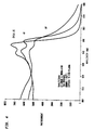
- FIG. 4 shows normalized photocurrent spectra obtained at different bias voltages. A voltage-dependent photocurrent response was detected below 5 volts, presumably because carrier sweep out from the wells was inhibited by non-radiative centers. The normalized spectra show that Quantum Confined Stark Shifts indeed occur at low voltages. Moreover, their quality was sufficiently high for the devices to support systems operating at ⁇ o (unbiased exciton).
Landscapes
- Physical Deposition Of Substances That Are Components Of Semiconductor Devices (AREA)
- Semiconductor Lasers (AREA)
- Logic Circuits (AREA)
Applications Claiming Priority (2)
| Application Number | Priority Date | Filing Date | Title |
|---|---|---|---|
| US284026 | 1994-08-01 | ||
| US08/284,026 US5589404A (en) | 1994-08-01 | 1994-08-01 | Monolithically integrated VLSI optoelectronic circuits and a method of fabricating the same |
Publications (2)
| Publication Number | Publication Date |
|---|---|
| EP0696064A2 true EP0696064A2 (de) | 1996-02-07 |
| EP0696064A3 EP0696064A3 (de) | 1997-09-03 |
Family
ID=23088578
Family Applications (1)
| Application Number | Title | Priority Date | Filing Date |
|---|---|---|---|
| EP95305041A Withdrawn EP0696064A3 (de) | 1994-08-01 | 1995-07-19 | Monolithisch integrierte VLSI, optoelektronische Schaltkreise und Herstellungsverfahren für diese |
Country Status (4)
| Country | Link |
|---|---|
| US (1) | US5589404A (de) |
| EP (1) | EP0696064A3 (de) |
| JP (1) | JPH0864798A (de) |
| CA (1) | CA2151658C (de) |
Families Citing this family (1)
| Publication number | Priority date | Publication date | Assignee | Title |
|---|---|---|---|---|
| US7206471B2 (en) * | 2004-12-23 | 2007-04-17 | Lucent Technologies Inc. | Integrated circuit having an optical core |
Family Cites Families (14)
| Publication number | Priority date | Publication date | Assignee | Title |
|---|---|---|---|---|
| US4862237A (en) * | 1983-01-10 | 1989-08-29 | Seiko Epson Corporation | Solid state image sensor |
| JPS6464044A (en) * | 1987-09-04 | 1989-03-09 | Fujitsu Ltd | Logical file processing system |
| CA1301897C (en) * | 1988-02-29 | 1992-05-26 | Goro Sasaki | Method for producing an opto-electronic integrated circuit |
| US5179029A (en) * | 1990-02-07 | 1993-01-12 | At&T Bell Laboratories | Hydrogen plasma passivation of GaAs |
| US5241198A (en) * | 1990-11-26 | 1993-08-31 | Matsushita Electronics Corporation | Charge-coupled device and solid-state imaging device |
| US5322811A (en) * | 1991-08-01 | 1994-06-21 | Canon Kabushiki Kaisha | Method for manufacturing a recording head with integrally housed semiconductor functional elements |
| JPH05110048A (ja) * | 1991-10-14 | 1993-04-30 | Mitsubishi Electric Corp | 光−電子集積回路 |
| KR950000522B1 (ko) * | 1991-11-25 | 1995-01-24 | 재단법인 한국전자통신연구소 | 수신용 광전집적 소자 및 그 제조방법 |
| US5273920A (en) * | 1992-09-02 | 1993-12-28 | General Electric Company | Method of fabricating a thin film transistor using hydrogen plasma treatment of the gate dielectric/semiconductor layer interface |
| US5314836A (en) * | 1992-09-15 | 1994-05-24 | Eastman Kodak Company | Method of making a single electrode level CCD |
| US5275687A (en) * | 1992-11-20 | 1994-01-04 | At&T Bell Laboratories | Process for removing surface contaminants from III-V semiconductors |
| US5379719A (en) * | 1993-07-26 | 1995-01-10 | Sandia National Laboratories | Method of deposition by molecular beam epitaxy |
| US5384267A (en) * | 1993-10-19 | 1995-01-24 | Texas Instruments Incorporated | Method of forming infrared detector by hydrogen plasma etching to form refractory metal interconnects |
| US5371038A (en) * | 1993-10-21 | 1994-12-06 | Motorola, Inc. | Method of forming a quantum multi-function semiconductor device |
-
1994
- 1994-08-01 US US08/284,026 patent/US5589404A/en not_active Expired - Lifetime
-
1995
- 1995-06-13 CA CA002151658A patent/CA2151658C/en not_active Expired - Fee Related
- 1995-07-19 EP EP95305041A patent/EP0696064A3/de not_active Withdrawn
- 1995-07-31 JP JP7212949A patent/JPH0864798A/ja active Pending
Non-Patent Citations (1)
| Title |
|---|
| "OSA Proceedings", 1993, SAN DIEGO, article K.V. SHENNOY ET AL., pages: 9433 |
Also Published As
| Publication number | Publication date |
|---|---|
| CA2151658C (en) | 2000-01-18 |
| JPH0864798A (ja) | 1996-03-08 |
| EP0696064A3 (de) | 1997-09-03 |
| US5589404A (en) | 1996-12-31 |
Similar Documents
| Publication | Publication Date | Title |
|---|---|---|
| USRE38072E1 (en) | Fabrication method for AlGaInNPAsSb based devices | |
| EP0544408B1 (de) | Lichtemittierende Halbleitervorrichtungen mit Quantenbegrenzung | |
| US4639275A (en) | Forming disordered layer by controlled diffusion in heterojunction III-V semiconductor | |
| US6566595B2 (en) | Solar cell and process of manufacturing the same | |
| US4594603A (en) | Semiconductor device with disordered active region | |
| US4511408A (en) | Semiconductor device fabrication with disordering elements introduced into active region | |
| US5837561A (en) | Fabrication of transparent substrate vertical cavity surface emitting lasers by semiconductor wafer bonding | |
| JP3425185B2 (ja) | 半導体素子 | |
| US5075743A (en) | Quantum well optical device on silicon | |
| JP3504742B2 (ja) | レーザダイオード | |
| US4843032A (en) | Process for producing a DFB laser with a diffraction grating superlattice | |
| JP3269558B2 (ja) | 青−緑レーザーダイオード | |
| US20030168653A1 (en) | Semiconductor light-emitting device, method for fabricating the same and optical disk apparatus | |
| US20060151794A1 (en) | Photonic crystal light emitting device | |
| US7501299B2 (en) | Method for controlling the structure and surface qualities of a thin film and product produced thereby | |
| KR20220140890A (ko) | 반도체 구조체 및 제작 방법 | |
| US10886429B2 (en) | Method of manufacturing an optoelectronic device by transferring a conversion structure onto an emission structure | |
| US20080014667A1 (en) | Modifying the optical properties of a nitride optoelectronic device | |
| EP0077825B1 (de) | Verfahren zur herstellung einer zone mit grossem bandabstand innerhalb mehrschichten halbleiter | |
| KR100601115B1 (ko) | 베릴륨-텔루륨 버퍼 층을 구비한 ⅱ-ⅵ족 반도체 장치 | |
| US6081001A (en) | Nitride semiconductor light emitting device | |
| JPH0766984B2 (ja) | ヘテロ超格子pn接合 | |
| US5589404A (en) | Monolithically integrated VLSI optoelectronic circuits and a method of fabricating the same | |
| JPH03236276A (ja) | 光機能素子 | |
| FR2547677A1 (fr) | Transistor bipolaire a double heterojonction compatible avec des composants optoelectroniques pour l'integration monolithique |
Legal Events
| Date | Code | Title | Description |
|---|---|---|---|
| PUAI | Public reference made under article 153(3) epc to a published international application that has entered the european phase |
Free format text: ORIGINAL CODE: 0009012 |
|
| AK | Designated contracting states |
Kind code of ref document: A2 Designated state(s): DE FR GB |
|
| PUAL | Search report despatched |
Free format text: ORIGINAL CODE: 0009013 |
|
| RHK1 | Main classification (correction) |
Ipc: H01L 27/15 |
|
| AK | Designated contracting states |
Kind code of ref document: A3 Designated state(s): DE FR GB |
|
| 17P | Request for examination filed |
Effective date: 19980211 |
|
| 17Q | First examination report despatched |
Effective date: 20010514 |
|
| STAA | Information on the status of an ep patent application or granted ep patent |
Free format text: STATUS: THE APPLICATION IS DEEMED TO BE WITHDRAWN |
|
| 18D | Application deemed to be withdrawn |
Effective date: 20020611 |