EP0690583A2 - Analog-Digitalwandler mit hoher Geschwindigkeit und anstiegsgeschwindigkeitskontrollierten Pulsdetektor - Google Patents
Analog-Digitalwandler mit hoher Geschwindigkeit und anstiegsgeschwindigkeitskontrollierten Pulsdetektor Download PDFInfo
- Publication number
- EP0690583A2 EP0690583A2 EP95109388A EP95109388A EP0690583A2 EP 0690583 A2 EP0690583 A2 EP 0690583A2 EP 95109388 A EP95109388 A EP 95109388A EP 95109388 A EP95109388 A EP 95109388A EP 0690583 A2 EP0690583 A2 EP 0690583A2
- Authority
- EP
- European Patent Office
- Prior art keywords
- input
- pulse
- signal
- amplifier
- output
- Prior art date
- Legal status (The legal status is an assumption and is not a legal conclusion. Google has not performed a legal analysis and makes no representation as to the accuracy of the status listed.)
- Ceased
Links
- 239000003990 capacitor Substances 0.000 claims description 9
- 238000000034 method Methods 0.000 claims description 8
- 238000001514 detection method Methods 0.000 claims description 4
- 238000005259 measurement Methods 0.000 claims 3
- 230000001934 delay Effects 0.000 claims 2
- 230000000694 effects Effects 0.000 description 5
- 239000006185 dispersion Substances 0.000 description 4
- 230000005540 biological transmission Effects 0.000 description 3
- 238000012937 correction Methods 0.000 description 3
- 230000003287 optical effect Effects 0.000 description 3
- 238000002310 reflectometry Methods 0.000 description 3
- 238000003491 array Methods 0.000 description 2
- 230000002238 attenuated effect Effects 0.000 description 2
- 230000001186 cumulative effect Effects 0.000 description 2
- 239000013307 optical fiber Substances 0.000 description 2
- 239000003570 air Substances 0.000 description 1
- 238000006243 chemical reaction Methods 0.000 description 1
- 238000004891 communication Methods 0.000 description 1
- 230000007547 defect Effects 0.000 description 1
- 238000000691 measurement method Methods 0.000 description 1
- 238000012545 processing Methods 0.000 description 1
- 230000000630 rising effect Effects 0.000 description 1
- 230000001360 synchronised effect Effects 0.000 description 1
- XLYOFNOQVPJJNP-UHFFFAOYSA-N water Substances O XLYOFNOQVPJJNP-UHFFFAOYSA-N 0.000 description 1
Images


Classifications
-
- G—PHYSICS
- G01—MEASURING; TESTING
- G01S—RADIO DIRECTION-FINDING; RADIO NAVIGATION; DETERMINING DISTANCE OR VELOCITY BY USE OF RADIO WAVES; LOCATING OR PRESENCE-DETECTING BY USE OF THE REFLECTION OR RERADIATION OF RADIO WAVES; ANALOGOUS ARRANGEMENTS USING OTHER WAVES
- G01S7/00—Details of systems according to groups G01S13/00, G01S15/00, G01S17/00
- G01S7/02—Details of systems according to groups G01S13/00, G01S15/00, G01S17/00 of systems according to group G01S13/00
- G01S7/28—Details of pulse systems
- G01S7/285—Receivers
-
- H—ELECTRICITY
- H03—ELECTRONIC CIRCUITRY
- H03K—PULSE TECHNIQUE
- H03K5/00—Manipulating of pulses not covered by one of the other main groups of this subclass
- H03K5/22—Circuits having more than one input and one output for comparing pulses or pulse trains with each other according to input signal characteristics, e.g. slope, integral
- H03K5/24—Circuits having more than one input and one output for comparing pulses or pulse trains with each other according to input signal characteristics, e.g. slope, integral the characteristic being amplitude
-
- H—ELECTRICITY
- H03—ELECTRONIC CIRCUITRY
- H03M—CODING; DECODING; CODE CONVERSION IN GENERAL
- H03M1/00—Analogue/digital conversion; Digital/analogue conversion
- H03M1/12—Analogue/digital converters
- H03M1/34—Analogue value compared with reference values
- H03M1/36—Analogue value compared with reference values simultaneously only, i.e. parallel type
- H03M1/361—Analogue value compared with reference values simultaneously only, i.e. parallel type having a separate comparator and reference value for each quantisation level, i.e. full flash converter type
- H03M1/362—Analogue value compared with reference values simultaneously only, i.e. parallel type having a separate comparator and reference value for each quantisation level, i.e. full flash converter type the reference values being generated by a resistive voltage divider
- H03M1/365—Analogue value compared with reference values simultaneously only, i.e. parallel type having a separate comparator and reference value for each quantisation level, i.e. full flash converter type the reference values being generated by a resistive voltage divider the voltage divider being a single resistor string
-
- G—PHYSICS
- G01—MEASURING; TESTING
- G01S—RADIO DIRECTION-FINDING; RADIO NAVIGATION; DETERMINING DISTANCE OR VELOCITY BY USE OF RADIO WAVES; LOCATING OR PRESENCE-DETECTING BY USE OF THE REFLECTION OR RERADIATION OF RADIO WAVES; ANALOGOUS ARRANGEMENTS USING OTHER WAVES
- G01S7/00—Details of systems according to groups G01S13/00, G01S15/00, G01S17/00
- G01S7/02—Details of systems according to groups G01S13/00, G01S15/00, G01S17/00 of systems according to group G01S13/00
- G01S7/40—Means for monitoring or calibrating
- G01S7/4004—Means for monitoring or calibrating of parts of a radar system
- G01S7/4021—Means for monitoring or calibrating of parts of a radar system of receivers
Definitions
- This invention relates to pulse detectors, in particular, pulse detectors with analog to digital (A/D) convertors and slew rate detection circuits.
- A/D analog to digital
- Optical and other electromagnetic pulses are used to transmit information and to detect objects at a distance from the transmitter.
- the detector receives pluses that have traveled through one or more mediums, e.g.., optical fibers, air, water, or space.
- the transmitted pulses are affected by the medium and the process of transmission. often the medium will result in a dispersion of the pulse, thereby attenuating its amplitude and spreading its energy over a wider pulse width than the original pulse width.
- Pulses are also affected by reflection from a target, as in the case of laser range finder pulses and radar. Some targets have low reflectivity and will attenuate and disperse a pulse.
- the pulse detector must detect pulses of various amplitudes and of various dispersions.
- Pulse detectors use an A/D converter to convert the amplitude of the detected pulse into a digital signal that can be processed by further digital circuitry to extract information from the detected pulse. It is also desireable to measure other characteristics of the pulse including arrival time and pulse width. Since many of the pulses are generated at high frequencies, the A/D converter must complete coversion of the pulse before the next pulse arrives. So, the A/D converter has to be faster in operation than the frequency of the pulse. Since pulses in optical system often exceed 100 megahertz, a high speed A/D converter is required.
- A/D converter operates on a continual basis. Such continual type converters generally are used for converting signals having a relatively slow frequency. It is possible to increase the speed of continual type converters, however an increase in speed necessarily requires a large increase in power, which is undesirable.
- A/D converter is a flash converter with a clocked architecture.
- the input signal is sampled and held until the data is converted.
- Flash converters require precise knowledge of when the data arrives. Flash converters are synchronized to the incoming data. Such clocked flash converters are not suitable for converting analog signals that arrive assynchronously or at a random time.
- Arrival time is measured by using a threshold value.
- the time of threshold crossing is taken as an indication that a pulse has arrive. So long as all pulses have the same dispersion, the threshold crossing technique will give an acceptable value of the arrival time.
- such measurement techniques present problems when pulses are not symmetrical or when the pulse is subject to transmission medium distortion. Another problem arises due to the amplitude of a pulse.
- Pulses generated by lasers or other optical communication systems normally are Gaussian pulses and have a center point that is well defined by their width. However, the amplitude of the pulse will vary depending upon the medium in which it is transmitted, including the dispursion within the medium and the distance of transmission. A typical Gaussian pulse generated optically will be attenuated by cloud cover or defects in the optical fiber which will tend to disperse the pulse as a function of distance.
- a detector will receive pulses of various widths and different heights. Since it is virtually impossible to detect the peak of a given pulse, then the presence of a pulse is normally detected by crossing of the threshold.
- a problem with detecting pulses using such a technique is illustrated with reference to prior art Fig. 4a. That figure shows two pulses A, B that arrive at the time but will appear to a threshold detector to arrive at different times.
- Pulse A is well defined, has a steep rise and has peak value of about 3.0 volts.
- Pulse B has a less steep rise and has a peak value of about 0.9 volts.
- the threshold voltage is 750 millivolts and the pulses will trigger the threshold at different times.
- Pulse A appears to arrive at a time T1 and Pulse B appears to arrive T2.
- the difference, T2-T1 is the amplitude induced error.
- the amplitudes of the respective pulses A, B induce error since the different amplitudes give an erroneous indication of the arrival time of the pulses.
- the larger pulse A appears to arrive substantially earlier than the smaller pulse B when, in fact, both pulses arrive at exactly the same time.
- the present invention includes an analog to digital converter comprising: a plurality of comparators, each having a reference input, an analog signal input for receiving a analog input signal, a reset input line and a bias input and an output for providing a digital output signal when the input analog signal equals the reference input and a hysteresis circuit for delaying the output of the comparator from falling when the input signal falls and responsive to a reset input signal for removing the analog signal from the signal input of the comparators.
- the present invention also includes a method for detecting the arrival time of each pulse signal in a sequence of pulse signals and limiting error induced by amplitude variations of the pulse signals as claimed in claim 4 comprising the steps of receiving an input signal of unknown amplitude, providing an amplifier with a controllable slew rate for comparing the amplitude of the input signal to a predetermined threshold, controlling slew rate of the amplifier so that the slew rate is less than the rate of change of signals of the largest amplitudes and sufficient to permit signals of a predetermined minimum amplitude to exceed the threshold, measuring the time when the input signal crosses said predetermined threshold to determine the arrival time of said signal.
- the invention provides a combined A/D converter and slew limiting pulse detector that converts high speed pulse signals into digital signals and gives an output signal representative of a more accurate arrival time of the converted, incoming pulses.
- the A/D converter has an architecture that includes a plurality of comparators with built-in hysteresis.
- the comparators have a bias circuit which sets all the comparators on the edge of their trigger voltage.
- Each comparator also has a reset input terminal. The smallest input above the trigger voltage of the comparator will cause the comparator to trigger as the voltage on the input cross the trigger voltage level.
- Each comparator is constructed with relatively large hysteresis so that when the pulse falls, the comparator holds its value.
- a pulse applied to the row of comparators is captured until the comparators are reset by applying a reset signal to their reset input. It is not necessary to synchronize the operation of-the A/D Converter with the incoming pulses. All that is required is knowledge of the range of frequencies of the input pulses. once that is known, the reset signal can be set to operate in a time longer than the expected pulse width but shorter than the pulse frequency. So, each input pulse is converted to a digital output and the comparator is reset before the next pulse arrives. As such, the reset timing can be based upon a standard cycle time. Another alternative is to reset the comparators after a predetermined amount of time that is greater than the width of the pulse. So, if a pulse was 5 nanoseconds wide than the comparator would be reset at a time greater than 5 nanoseconds, e.g. 10 nanoseconds.
- the slew rate limiting pulse detector of the invention limits the error induced by the amplitude of the incoming pulses.
- the slew rate limiting pulse detector includes a comparator amplifier with an input terminal for receiving input pulses of various heights. The comparator is set with a predetermined, programmable threshold for detecting pulses of a minimum amplitude.
- the amplifier has a controlled slew rate.
- the slew rate is also programmable but may be fixed.
- the slew rate of the amplifier is preferably set to have a rate fast enough to detect pulses of the smallest allowable magnitude. By controlling the slew rate to detecting pulses of the smallest allowable magnitude, errors introduced by sharper, higher amplitude pulses, will be limited.
- the slew rate control will, in effect, dampen the rise time of the pulses. So, large amplitude pulses will appear to arrive later in time, e.g. at a time closer to the arrival time indicated by a the lower amplitude pulses. Thus, the error introduced by the amplitude of incoming pulses will be substantially reduced.
- the slew rate is controlled by modulating the current through a capacitor which sets the slew rate of the comparator. As such, one may modulate the capacitor or the capacitor's value, or the current through the capacitor. In either case, it is the product of the current and the capacitance that sets the slew rate for the amplifier.
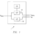
- Fig. 1 depicts a general description of the system and circuitry of the invention.
- a pulse in the form of a voltage pulse identified as V PULSE is input to the A/D arrival time pulse detector system 1.
- the input, V PULSE is simultaneously applied to an A/D converter 10 and to an arrival time detector 110.
- the A/D converter 10 has an output V DIGITAL that is a binary signal representative of the maximum value of the V PULSE
- the second output, V AT has also a binary signal representative of arrival time of the signal V PULSE at the system 1.
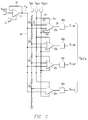
- Figure 2 shows the A/D convertor 10 with a buffer amplifier 14 and a plurality of comparators 30.
- the signal V PULSE is input to a buffer amplifier 14.
- the buffer amplifier 14 has a feedback connection 16 to another input and has a bias input 12.
- the output of buffer amplifier 14 is the signal V IN .
- the signal V IN is applied to line 18. Coupled to line 18 are n numbers of comparators 30a, 30b, 30c unlike 30n.
- a string of n resistors 20a, 20b, 20c across 20n each of selectable value are connected to the negative inputs of the comparators 30n.
- V REF Connected to one end of the string of resistors 20n is a voltage of a known value, V REF
- Thevalue of V REF is selected to be compatible with the expected value of the input signal V PULSE . As such, if the maximum expected amplitude of V PULSE is 3 volts, then the reference voltage V REF is greater than 3 volts e.g. 4 volts.
- the number of comparators 30n and selectableresistors 20n depends upon the degree of accuracy desired from the A/D converter 10. The preferred embodiment of the invention has 3+ bit accuracy and thus there are 14 comparator 30 resistors 20a. Each comparator 30 has a bias input 31.
- a bias voltage V BIAS is coupled via line 22 to each of the bias inputs 31n of the comparators 30n.
- Each comparator 30 has a further reset input 34.
- a reset signal V RESET is coupled via line 24 to each of the reset inputs 34n of the comparators 30n.
- Logic level shifters 40n provide output digital logic signals compatible withcircuit processing. Taken together, the respective outputs V1 OUT V2 OUT . . . V N OUT provide the digital output V DIGITAL of the A/D converter 10.
- an input signal V PULSE is applied via buffer 14 to input line 18.
- Each comparator 30 is set at its edge of triggering by its bias input 31. Normally the comparator outputs 34 would tend to follow the pulse and thus would fall after the pulse passes its peak. However, each comparator 30n includes a circuit which increases the hysteresis of the comparator to delay the comparator from following the pulse as the pulse falls in amplitude.
- a reset signal V RESET is applied to reset line 24 and the A/D converter is reset so that its output is set to zero.
- Fig. 3 shows a typical comparator 30.
- inputs 303 and 306 are the plus andminus inputs to the comparator 30.
- the plus input 303 is coupled to the comparator via a transistor 306.
- the minus input 306 is coupled via another transistor 303.
- the minus input 306 is coupled to a reference voltage applied to a resistor 20.
- the plus and minus inputs 303, 306 of the comparator 30 are coupled to a first differential pair of transistors of 304 and 305.
- the output of the differential pair of transistors 304 and 305 is coupled via a first FET transistor 308 to ground.
- FET transistor 308 along with other FET transistors 307, 309, 310, 311 and 336-339 each provide a bias current as will be explained herein after. By applying a VBIAS to the gates of transistors 307-311 and 336-339 those FET transistors are controlled to draw a certain predetermined amount of bias current.
- the first differential pair 304,.305 of npn transistors are level shifters. These transistors shift 35 the level of input voltage to a level of voltagecompatible to the rest of the circuitry.
- a second set of differential pairs 318, 319 are coupled, respectively, toresistors 314, 315. Resistors 314 and 315 are coupled via transistors 312, 313 to the collectors of the first differential pair 304, 305. As such, the inputs 303, 306 are coupled to the respective bases of the seconddifferential pair of npn transistors 318, 319.
- transistors 312, 313 are followers that couple the input differential pair 304, 305 to the operational differential pair 318, 319.
- the collectors of differential pair 318, 319 are connected to the bases, respectively, of npn transistors 330, 331.
- Transistors 330, 331 are connected as followers.
- the output of transistor 330 is connected to a first pair of diodes 332, 333.
- the output of transistor 331 is coupled to a second pair of diodes 334, 335.
- the outputs of the diode pairs 332-335 are themselves connected to a third differential pair of transistors 341, 342.
- Diode pair 332, 333 is coupled to the output and also to the base of npn transistor 342.
- Diode pair 334, 335 is coupled to the minus V OUTPUT and also to the base of npn transistor 341.
- Differential pair of transistors 341, 342 provide hysteresis for the comparator 30.
- the second differential pair of transistors 318, 319 triggers and the output go high, the minus output of the second differential pair is pulled down by the transistor 341. So, the outputs of the second differential pair 318, 319 will remain fixed until the comparator 30 is reset. Reset is accomplished by applying the signal V RESET to transistor 343.
- Transistor 343 turns on and this turns off the hysteresis differential pair 341, 342. That pair releases the minus output Vout and allows the comparator 30 to return to normal operation.
- Fig. 4 shows two pulses, A I and B'.
- the trigger level for the pulses is set at 750millivolts.
- the amplitude of pulse A' is about 2.8 volts and pulse B' is approximately 0.9 volts.
- the slew rate of the pulse detector 110 is set at approximately 150 volts per microsecond.
- the arrival of either pulse A' or pulse B' is determined at the time the pulse passes the 750mv threshold level.
- the slew rate limited pulse detector 110 has a slew rate of 150 volts per microsecond.
- the amplitude may be attenuated due to dispersion or may be greater than expected due to enhanced reflectivity from nearby objects.
- systems are designed to detect pulses of minimum and maximum heights.
- the threshold trigger level here 750mv
- the threshold level is set to detect thelowest level of pulse available.
- the maximum level of pulse may well exceed the minimum level and thereby induce arrival time error. So, pulse A' without slew correction would appear to arrive at time T1 and pulse B' would arrive at time T3.
- the rise time of pulse A' is limited to the slope defined by the slew limit.
- Pulse A' is forced to follow the slew limit of 150v/msec and will have an apparent arrival time of T2 and the error in arrival time between the two pulses is T3-T2.
- the slew limit of150v/msec can be set accurately. It has been determined that the slew limit rate of the preferred embodiment is the maximum rate of change of the smaller pulse. Thus, the slew limit shown in Fig. 4 appears to be parallel to a major portion of the rising slope of pulse B'.
- the slew limit pulse detector 110 With reference to Fig. 5, there is shown the slew limit pulse detector 110.
- the input V PULSE is provided to a slew controlled amplifier 120.
- the amplifier 120 is a differential amplifier having differential inputs 124, 125, a bias, input 123 and a slew limit control input 119.
- the slew limit control input 119 comes from a slew limit controller 121.
- Slew limit controller 121 comprises a network of programmable or otherwise configurablecircuits which set the slew rate for the amplifier 120. Those skilled in the art are familiar with controlling the slew limit of amplifiers and a further description is not necessary to enable one skilled in the art to makeclaimed invention.
- the slew rate can be limited from one to four times its normal rate.
- the slew limit controller 121 changes the current through a capacitor (not shown) which in turn controls the current into theslew limit input 119 of the slew limit amplifier 120.
- the output of the slew limit amplifier, V SOUT at mode 126 is input into a comparator 130.
- the comparator 130 had an amplifier 135 with an input from a programmable reference generator 131 and a reset controller 132. itshould be noted that the input V PULSE may bypass the amplifier 120 and be applied directly to the comparator 130. This is accomplished by operation of one or more of the switches 113, 114.
- the output of amplifier 135 is coupled into an output controller 134 which in turn has a feedback connection to amplifier 135.
- the output controller 134 is coupled to a timer 140.
- the output of timer 140 provides a signal V AT which is representative of the arrival time of the V PULSE signal.
- the timer 140 is a high speed counter. Its output V AT is a logical levelsignal that includes binary representation of the arrival time of the signal V PULSE .
- Comparator 130 has programmable bias input 131 for a setting of threshold level.
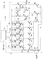
- the amplifier 120 is shown if further detail along with further details of theslew controller 121.
- slew controller 121 receives an input signal V SLEW SELECT .
- the signal V SLEW SELECT is input to a suitable multiplexer 127.
- Multiplexer 127 has a plurality of output lines 200-204. Each output line controls two of the switches in the switch arrays 210-214 and 230-234. As such, multiplex line output 200 controls switches 210 and 230; line 201 controls switches 211 and 231, etc.
- The.switches 210-214 and 230-234 control the amount of current passing through transistors 220-225.
- transistor 220 is coupled between its pair of control switches 210 and 230.
- Transistors 211-225 are likewise coupled between their respective pair of controls switches, from the remaining switches 211-215 and 231-235.
- the output currents of transistors 220-225 are summed by summing transistors 240-244.
- the summed currents are applied via transistors 294-295 as a control current signal 119 to the coupled emitters of a first differential pair of transistors 260, 261.
- a second differential pair of transistors 250, 251 has the gate of transistor 250 shorted to its drain and the drain of the other transistor 251 coupled to capacitor 271.
- the current in transistor 295 controls how much current is drawn by the differential pair 260, 261 which make up the plus and minus inputs 124, 125 of the amplifier 120. That current is suitably controlled when the V SLEW SELECT signal applied to the multiplexer 127 which operates the switch arrays 210-214, 230-234, and transistors 220-224, 240-244.
- the current on line 119 controls the slew rate of the amplifier and it set by the signal V SLEW SELECT .
- a pulse detecting system 1 has a high speed A/D converter 10 and a slew controlled pulse detector 110.
- the A/D converter 10 has large hysteresis for holding the converted digital value of an Input signal V PULSE until the A/D converter 10 is reset.
- the slew controlled pulse detector 110 limits the slew rate of large amplitude pulse to correct arrival errors and provide an output signa V AT that more accurately represents the arrival time of the input pulse signal, V PULSE .
Landscapes
- Engineering & Computer Science (AREA)
- Physics & Mathematics (AREA)
- Nonlinear Science (AREA)
- Theoretical Computer Science (AREA)
- Computer Networks & Wireless Communication (AREA)
- General Physics & Mathematics (AREA)
- Radar, Positioning & Navigation (AREA)
- Remote Sensing (AREA)
- Analogue/Digital Conversion (AREA)
- Measurement Of Unknown Time Intervals (AREA)
- Radar Systems Or Details Thereof (AREA)
- Manipulation Of Pulses (AREA)
Applications Claiming Priority (2)
| Application Number | Priority Date | Filing Date | Title |
|---|---|---|---|
| US08/269,470 US5808489A (en) | 1994-06-30 | 1994-06-30 | High speed A/D converter and slew controlled pulse detector |
| US269470 | 1994-06-30 |
Publications (2)
| Publication Number | Publication Date |
|---|---|
| EP0690583A2 true EP0690583A2 (de) | 1996-01-03 |
| EP0690583A3 EP0690583A3 (de) | 1996-08-07 |
Family
ID=23027393
Family Applications (1)
| Application Number | Title | Priority Date | Filing Date |
|---|---|---|---|
| EP95109388A Ceased EP0690583A3 (de) | 1994-06-30 | 1995-06-16 | Analog-Digitalwandler mit hoher Geschwindigkeit und anstiegsgeschwindigkeitskontrollierten Pulsdetektor |
Country Status (3)
| Country | Link |
|---|---|
| US (1) | US5808489A (de) |
| EP (1) | EP0690583A3 (de) |
| JP (1) | JPH0865162A (de) |
Families Citing this family (1)
| Publication number | Priority date | Publication date | Assignee | Title |
|---|---|---|---|---|
| US6816816B2 (en) * | 2003-02-12 | 2004-11-09 | Bently Nevada, Llc | Transducer fault detection system using slew rate measurements: apparatus and method |
Family Cites Families (9)
| Publication number | Priority date | Publication date | Assignee | Title |
|---|---|---|---|---|
| US3392386A (en) * | 1967-02-23 | 1968-07-09 | Hughes Aircraft Co | Multilevel digital skimmer |
| US3725673A (en) * | 1971-08-16 | 1973-04-03 | Motorola Inc | Switching circuit with hysteresis |
| DE2944657C2 (de) * | 1979-11-06 | 1985-02-14 | Robert Bosch Gmbh, 7000 Stuttgart | Komparatorschaltung |
| US4874969A (en) * | 1988-06-08 | 1989-10-17 | National Semiconductor Corporation | High speed CMOS comparator with hysteresis |
| EP0417334B1 (de) * | 1989-09-11 | 1993-12-29 | Siemens Aktiengesellschaft | Kippschaltung mit Schalthysterese |
| DE4005037A1 (de) * | 1990-02-16 | 1991-08-22 | Siemens Nixdorf Inf Syst | Verfahren zum umsetzen einer analogen spannung in einen digitalwert |
| US5083124A (en) * | 1990-04-17 | 1992-01-21 | Teleco Oilfield Services Inc. | Nuclear logging tool electronics including programmable gain amplifier and peak detection circuits |
| JP3159331B2 (ja) * | 1992-03-31 | 2001-04-23 | ソニー株式会社 | 信号入力判定装置及び比較回路 |
| US5367203A (en) * | 1993-01-21 | 1994-11-22 | Brooktree Corporation | System for determining the time at which an analog voltage crosses a voltage threshold |
-
1994
- 1994-06-30 US US08/269,470 patent/US5808489A/en not_active Expired - Lifetime
-
1995
- 1995-06-16 EP EP95109388A patent/EP0690583A3/de not_active Ceased
- 1995-06-29 JP JP7164099A patent/JPH0865162A/ja active Pending
Non-Patent Citations (1)
| Title |
|---|
| None |
Also Published As
| Publication number | Publication date |
|---|---|
| EP0690583A3 (de) | 1996-08-07 |
| JPH0865162A (ja) | 1996-03-08 |
| US5808489A (en) | 1998-09-15 |
Similar Documents
| Publication | Publication Date | Title |
|---|---|---|
| US5262837A (en) | Laser range finder | |
| US4017856A (en) | Self-calibrating microwave transponder | |
| US4695752A (en) | Narrow range gate baseband receiver | |
| US5563893A (en) | Integrated level detector | |
| JPH1123709A (ja) | 距離測定装置 | |
| US4694200A (en) | Device for detecting a pulse train in noise and application to a radionavigation aid system of DME type | |
| US5221928A (en) | Method and apparatus for accurate, high speed pulse-echo measurement calibration | |
| US5637994A (en) | Waveform measurement | |
| US6646479B1 (en) | Pulse discriminator | |
| US3509558A (en) | Wide range data compression system | |
| US5102219A (en) | Method and means in optical distance meters | |
| WO1982000931A1 (en) | A method and an arrangement for increasing the dynamic range at the input stage of a receiver in an optical fibre information transmission system | |
| KR100310791B1 (ko) | 레이저 거리 측정 장치 | |
| US5808489A (en) | High speed A/D converter and slew controlled pulse detector | |
| US4786168A (en) | Frequency domain laser velocimeter signal processor | |
| US4904947A (en) | Method and circuit for measuring pulse width | |
| JPH11160432A (ja) | 光パルスレーダ装置及び光パルス受光装置 | |
| RU2097922C1 (ru) | Приемник импульсных радиосигналов и измеритель уровня для него | |
| US4320289A (en) | Precision laser pulse radiometer | |
| SE440155B (sv) | Anleggning for angivande av avstand till mal | |
| US4571514A (en) | Amplitude adjusted pulse width discriminator and method therefor | |
| US4408895A (en) | Apparatus for accurately timing an event relative to clock signals | |
| US5382848A (en) | Digital integrated time of arrival detector | |
| US3392386A (en) | Multilevel digital skimmer | |
| US2977538A (en) | Phase measuring system |
Legal Events
| Date | Code | Title | Description |
|---|---|---|---|
| PUAI | Public reference made under article 153(3) epc to a published international application that has entered the european phase |
Free format text: ORIGINAL CODE: 0009012 |
|
| AK | Designated contracting states |
Kind code of ref document: A2 Designated state(s): DE FR GB IT SE |
|
| 17P | Request for examination filed |
Effective date: 19951208 |
|
| PUAL | Search report despatched |
Free format text: ORIGINAL CODE: 0009013 |
|
| AK | Designated contracting states |
Kind code of ref document: A3 Designated state(s): DE FR GB IT SE |
|
| 17Q | First examination report despatched |
Effective date: 20000208 |
|
| GRAG | Despatch of communication of intention to grant |
Free format text: ORIGINAL CODE: EPIDOS AGRA |
|
| STAA | Information on the status of an ep patent application or granted ep patent |
Free format text: STATUS: THE APPLICATION HAS BEEN REFUSED |
|
| 18R | Application refused |
Effective date: 20020211 |