EP0689366B1 - Telephonic tone detection circuit - Google Patents
Telephonic tone detection circuit Download PDFInfo
- Publication number
- EP0689366B1 EP0689366B1 EP95410049A EP95410049A EP0689366B1 EP 0689366 B1 EP0689366 B1 EP 0689366B1 EP 95410049 A EP95410049 A EP 95410049A EP 95410049 A EP95410049 A EP 95410049A EP 0689366 B1 EP0689366 B1 EP 0689366B1
- Authority
- EP
- European Patent Office
- Prior art keywords
- processing units
- memory
- signal
- values
- addresses
- Prior art date
- Legal status (The legal status is an assumption and is not a legal conclusion. Google has not performed a legal analysis and makes no representation as to the accuracy of the status listed.)
- Expired - Lifetime
Links
Images

Classifications
-
- H—ELECTRICITY
- H04—ELECTRIC COMMUNICATION TECHNIQUE
- H04Q—SELECTING
- H04Q1/00—Details of selecting apparatus or arrangements
- H04Q1/18—Electrical details
- H04Q1/30—Signalling arrangements; Manipulation of signalling currents
- H04Q1/44—Signalling arrangements; Manipulation of signalling currents using alternate current
- H04Q1/444—Signalling arrangements; Manipulation of signalling currents using alternate current with voice-band signalling frequencies
- H04Q1/45—Signalling arrangements; Manipulation of signalling currents using alternate current with voice-band signalling frequencies using multi-frequency signalling
- H04Q1/457—Signalling arrangements; Manipulation of signalling currents using alternate current with voice-band signalling frequencies using multi-frequency signalling with conversion of multifrequency signals into digital signals
-
- H—ELECTRICITY
- H04—ELECTRIC COMMUNICATION TECHNIQUE
- H04Q—SELECTING
- H04Q1/00—Details of selecting apparatus or arrangements
- H04Q1/18—Electrical details
- H04Q1/30—Signalling arrangements; Manipulation of signalling currents
- H04Q1/44—Signalling arrangements; Manipulation of signalling currents using alternate current
Definitions
- the present invention relates to a modular structure programmable to detect various telephone tones which vary from one standard of telephone transmission to another and from one country to another.
- the present invention more generally relates to the detection of identification signals in a digital signal to using a set of processing modules which can be programmatically interconnected by a user.
- a identification signal is generally characterized by a amplitude exceeding, at a predetermined frequency, a threshold or the amplitude of another identification signal.
- the processing modules include filters programmable, rectification and integration modules (power estimators), and comparators.
- Rockwell company markets detection circuit tone including three times serial association a programmable filter, a power estimator, and a comparator.
- This tone detector has only two configurations programmable. In a first configuration, each of the three filters receives the digital signal to be processed, which can detect three different tones. In the second configuration, the three filters are connected in series in order to ability to detect a tone in a narrow frequency band.
- This structure which is known from document GB-A-2 255 472, is far from being able to adapt to all possible tone detection situations.
- An object of the present invention is to provide a programmable signal processing structure that can adapt to virtually any situation in the field in which programmable structure is used.
- Another object of the present invention is to achieve a structure particularly simple and easy to program.
- the present invention provides a circuit for detecting identification signals in an input digital signal which has values arriving at a sampling frequency, comprising a set of modules freely programmable interconnected processing units by a user; an updated signal memory at the sampling frequency of the input signal, containing the values of the output signals from the processing modules and the input signal to associated addresses; a programming memory containing, in locations associated with entries processing modules, addresses of the signal memory associated with the signals that the user wishes to connect to said starters; and control means for reading the addresses stored in the programming memory, read the values finding at these addresses in the signal memory, and providing these values read at the inputs of the processing modules in a order corresponding to the locations of the programming memory.
- the circuit includes an input memory in which the values read are stored in associated locations respectively at the inputs of the processing modules.
- the processing modules include first modules of processing and second processing modules to which are associated respectively a first programming memory and a second programming memory, the control means being intended to read the addresses stored in the first and second programming memories at different frequencies, read the values found at these addresses in the signal memory, and supply these values read to the inputs of the first processing modules and second processing modules in respective orders corresponding to the locations first and second programming memories.
- the circuit includes first and second input memories associated respectively with the first processing modules and to the second processing modules, in which the values read are stored in associated locations respectively at the inputs of the first and second processing modules processing modules.
- the first processing modules include programmable filters and recovery and integration modules
- second processing modules include comparators
- the signal memory also stores threshold values that the user can choose to provide comparators.
- processing module operations are performed by a programmable set for performing operations sequentially.
- the present invention provides a set of modules sufficient treatment and sufficient diversity to be able to adapt, by simple programming, the structure to all use cases of a predetermined domain. For it, the user should be able to program virtually any what interconnection of modules.
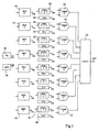
- FIG. 1 shows an overall example of processing modules of a programmable structure according to the invention adapted to the field of telephone transmissions.
- This set of modules includes a set of programmable filters (FILT) 10, a set of power estimation modules (PWR) 20, a set of modules 30 providing a value threshold VT, and a set of comparators (COMP) 32.
- An example programmable filter 10 and power estimation module 20 will be described later.
- FIG 1 there is shown eight modules, numbered 0 to 7, of each type.
- the exits comparators 32, providing detection signals of DET tone, are stored in a register (latch) 34.
- the digital signal to be processed Rx is available in a module 36, which is, for example, a register updated at the frequency sampling signal Rx.
- a value corresponding to GND ground potential is available in a module 38, which is, for example, made up of a set of bits forced into permanence to mass potential.
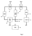
- FIG. 2 shows schematically a programmable structure according to the invention. Filters 10 and power estimators 20 are gathered in a block 50. The comparators 32 are gathered in a block 52.
- each signal is assigned, according to the invention, of a fixed address of a location of a signal memory 54.
- the address 00h (where the letter h means that the number is hexadecimal) at zero signal GND
- address 01h at signal input Rx addresses 10 a.m. to 5 p.m. at the outputs of filters 10, the addresses 8 p.m. to 7 p.m. at the outputs of the power estimators 20, and the addresses 30h to 37h at the threshold values VT.
- the locations of memory 54 are updated, to each sampling period, by the corresponding values of the outputs of the modules 50 and of the input signal Rx.
- the VT threshold values are written to their respective locations of memory 54, initially, for example at power up of the structure.
- the inputs of the modules 50 are associated respectively at fixed locations in a programming memory 56.
- a user writes (program) the address of the signal he wishes to apply to the module entry associated with the slot.
- each input of the comparators 52 is associated with a respective fixed location of a memory of programming 58 in which the user writes the addresses signals to provide to the comparators.
- Each input of the modules 50 is also associated with a respective fixed location of an input memory 60 in which we write the values to provide to modules 50.
- each input of the comparators 52 is associated with a location respective fixed of an input memory 62 in which one writes the values of the signals to be supplied to the comparators 52.
- a control circuit 64 manages the transfers between the different memories, as described below.
- the modules 50 perform their operations using values memory 60 and the results are transferred to the respective addresses in memory 54.
- the comparators 52 carry out the comparisons from the respective values stored in memory 62, and validate or not the respective bits of register 34 ( Figure 1).
- each address stored in memory 56 is examined and the value stored at this address in memory 54 is transferred to a corresponding location in memory 60. Readings in memory 56 are carried out in the same order that the entries in memory 60 so as to respect the correspondence between the locations of memories 56 and 60 and the inputs of the modules 50.
- each address stored in memory 58 is examined and the value stored at this address in memory 54 is transferred to a corresponding location in memory 62.
- the modules 50 and the comparators 52 carry out their operations with new values.
- Intermediate transfer of memory 54 to memories 60 and 62 realizes, according to one aspect of the invention, a delay in a sampling period which is used to avoid a drawback discussed below.
- the memories 60 and 62 are constituted by input registers modules 50 and 52.
- the signal memory 54 consists of output registers of modules 50, of registers containing the threshold values VT, and of the register containing the value to be processed of the Rx signal.
- the modules 50 are a set of modules operating in parallel or sequentially, or one or two elementary modules reprogrammed to perform sequentially the operations of all filtering and estimation modules power.
- the operations of modules 50 and 52 are performed in software and memories 54 to 62 form part of the same and single memory also storing programmable parameters filters and power estimators.
- FIGS. 3A and 3B show two examples of programming of interconnection between three modules MOD1 to MOD3.
- a signal S is, in the two cases of FIGS. 3A and 3B, processed successively by modules MOD1 to MOD3.
- MOD1 and MOD2 provide intermediate results R1 and R2, and the MOD3 module provides the final R3 result.
- module operations do not are not performed simultaneously. Especially if these operations are performed in software, they are performed sequentially.
- Figures 3A and 3B we have shown from top to bottom the modules in order of execution of their operations. In FIG. 3A, the operations are carried out in the order of modules MOD1 to MOD3, and in the figure 3B, they are carried out in the order of modules MOD3 to MOD1.
- FIGS. 4A and 4B illustrate, for the configurations of FIGS. 3A and 3B respectively, an example of evolution of the signals S and R1 to R3 in the order of execution of the operations of the modules MOD1 to MOD3.
- a sample of the signal S is provided at an instant t 0 . It is assumed, for simplicity, that each of the modules MOD1 to MOD3 is such that it transmits at its output the value present at its input when the operation of the module is carried out.
- each module performs its operation at a time when the previous module has supplied its result, that is to say that a module of FIG. 3A performs its operation when its entry is at value expected.
- the sample from input signal S is transmitted to output R3 without delay (except that of module operations, which is neglected).
- the operation of a module is performed while that of the previous module has not yet been.
- the input of the module considered is not at the expected value, except for the MOD1 module.
- the sample of the signal S is transmitted on the output R1.
- the operations of the MOD3 and MOD2 modules are carried out from time t 0 but before that of the MOD1 module; the outputs R3 and R2 are in any states,
- the operation of the module MOD2 is carried out while its input (R1) receives the sample of the signal S. This sample is transmitted on the output R2.
- the operation of the MOD3 module is carried out before that of the MOD2 module; the output R3 is in any state.
- the operation of the MOD3 module is carried out while the sample is present at the input (R2) of the MOD3 module; this sample is transmitted to output R3.
- one aspect of the invention is to introduce a delay of a sampling period in each module.
- FIGS. 5A and 5B respectively illustrate the behaviors thus obtained in the cases of FIGS. 3A and 3B.
- FIG. 5A illustrating the behavior of the configuration of FIG. 3A
- the sample of the signal S is successively transmitted to the outputs R1 to R3 with a delay of a sampling period at each transmission.
- the output R3 provides the sample at an instant t 3 following the instant t 0 of three sampling periods.
- FIG. 5B illustrating the behavior of the configuration of FIG. 3B, the same phenomenon as that described with the aid of FIG. 4B occurs, but with a delay sampling period. It follows that the transmitted sample is found on the output R3 at time t 3 , as in FIG. 5A. Thus, whatever the connection order of the modules, the signals are transmitted with the same delay.
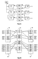
- FIGS 6A and 6B illustrate a programming example structure and corresponding contents of memories 54 to 62.
- the Rx signal, stored at address 01h in memory 54 is connected to filters 0 and 1 as well as to the power estimator 1.
- the locations of memory 56 associated with the filters 0 and 1 and to the power estimator 1 contain the address 01h.
- the output signal of filter 0, stored at address 10h in memory 54 is connected to the power estimator 0; the address 10h is stored in memory 56 at the location associated with the power estimator 0.
- the output signal from the filter 1, stored at address 11h in memory 54, is linked to filter 2; the address 11h is stored in memory 56 at the location associated with filter 2.
- the filter output signal 2, stored at the address 12h in memory 54, is connected to the power estimator 2; memory location 56 associated with the power estimator 2 contains the address 12h.
- the output signals of the power estimators 0 and 1, stored at addresses 8 p.m. and 9 p.m. in memory 54, are linked respectively to the first inputs (+) of the comparators 0 and 1, and the threshold values VT0 and VT1, stored at addresses 30h and 31h in memory 54, are provided respectively to the second inputs (-) of the comparators 0 and 1; the memory 58 stores the addresses 8 p.m. and 9 p.m. in locations associated with the first inputs of comparators 0 and 1, and stores the addresses 30h and 31h in locations associated with second inputs of comparators 0 and 1.
- the output signals power estimators 2 and 1 are provided respectively at the two comparator 2 inputs.
- the addresses 22h and 21h are stored in memory 58 at the locations associated with comparator inputs 2.
- the locations of the memories 60 and 62 are associated with the modules in the same order than the locations of programming memories 56 and 58.
- a each sample of the signal to be processed Rx, the addresses contained in programming memories 56 and 58 are read consecutively and the values contained at these addresses in the memory 54 are written in the same order in the memories input 60 and 62. So, for example, the Rx value contained in the address 01h from memory 54 is transferred to memory 60 the locations associated with filters 0 and 1 and the estimator of power 1.
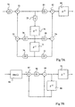
- Figures 7A and 7B show respective examples a filtering module and an estimation module of power.
- the filter module of FIG. 7A is a second order filter comprising two delay elements Z -1 70 and 71 arranged in series.
- the module 70 receives the output of an adder 72 via a multiplier by 2 73.
- a first input of the adder 72 receives the input signal from the filter via a multiplier 74 by a programmable coefficient C0.
- a second input of the adder 72 receives the output of an adder 75.
- the adder 75 receives on a first input the output of the delay element 71 via a multiplier 76 by a programmable coefficient C4 and on a second input the output of the delay element 70 via a multiplier 78 by a programmable coefficient C5.
- the outputs of the delay elements 70 and 71 are respectively supplied to the inputs of an adder 79 respectively via a multiplier 80 by a programmable coefficient C2 and a multiplier 81 by a programmable coefficient C1.
- the output of the adder 79 is supplied to a first input of an adder 82 which receives on a second input the output of the adder 72 via a multiplier 83 by a programmable coefficient C3.
- the output of the filter consists of the output of the adder 82.
- a delay element 84 connected to this output corresponds to the delay introduced according to the invention to avoid the drawback mentioned in connection with FIGS. 3A to 4B.
- the power estimator module shown in FIG. 7B comprises an element for calculating absolute value 86 which receives input from the module.
- Subtractor 87 provides the difference between the output of element 86 and an element of delay 88. This difference is supplied to an adder 89 by through a multiplier 90 by a programmable coefficient P1.
- the output of the adder 89, which constitutes the module output, is looped back to the second input of the adder 89 by the delay element 88.
- An element of delay 91 is arranged at the output of the module to obtain the delay avoiding the aforementioned drawback.
Description
La présente invention concerne une structure modulaire programmable pour détecter diverses tonalités téléphoniques qui varient d'une norme de transmission téléphonique à une autre et d'un pays à un autre.The present invention relates to a modular structure programmable to detect various telephone tones which vary from one standard of telephone transmission to another and from one country to another.
La présente invention vise plus généralement la détection de signaux d'identification dans un signal numérique à l'aide d'un ensemble de modules de traitement qui peuvent être interconnectés de manière programmable par un utilisateur. Un signal d'identification est généralement caractérisé par une amplitude excédant, à une fréquence prédéterminée, un seuil ou l'amplitude d'un autre signal d'identification. Pour détecter un tel signal, les modules de traitement comprennent des filtres programmables, des modules de redressement et d'intégration (estimateurs de puissance), et des comparateurs.The present invention more generally relates to the detection of identification signals in a digital signal to using a set of processing modules which can be programmatically interconnected by a user. A identification signal is generally characterized by a amplitude exceeding, at a predetermined frequency, a threshold or the amplitude of another identification signal. To detect a such signal, the processing modules include filters programmable, rectification and integration modules (power estimators), and comparators.
La société Rockwell commercialise un circuit de détection de tonalité comprenant trois fois l'association en série d'un filtre programmable, d'un estimateur de puissance, et d'un comparateur. Ce détecteur de tonalité a seulement deux configurations programmables. Dans une première configuration, chacun des trois filtres reçoit le signal numérique à traiter, ce qui permet de détecter trois tonalités différentes. Dans la deuxième configuration, les trois filtres sont reliés en série afin de pouvoir détecter une tonalité dans une bande de fréquence étroite. Cette structure qui est connue du document GB-A-2 255 472, est loin de pouvoir s'adapter à toutes les situations possibles de détection de tonalité.Rockwell company markets detection circuit tone including three times serial association a programmable filter, a power estimator, and a comparator. This tone detector has only two configurations programmable. In a first configuration, each of the three filters receives the digital signal to be processed, which can detect three different tones. In the second configuration, the three filters are connected in series in order to ability to detect a tone in a narrow frequency band. This structure which is known from document GB-A-2 255 472, is far from being able to adapt to all possible tone detection situations.
Un objet de la présente invention est de prévoir une structure programmable de traitement de signal qui puisse s'adapter à pratiquement toutes les situations du domaine dans lequel la structure programmable est utilisée.An object of the present invention is to provide a programmable signal processing structure that can adapt to virtually any situation in the field in which programmable structure is used.
Un autre objet de la présente invention est de réaliser une structure particulièrement simple et facile à programmer.Another object of the present invention is to achieve a structure particularly simple and easy to program.
Pour atteindre ces objets, la présente invention prévoit un circuit de détection de signaux d'identification dans un signal numérique d'entrée qui présente des valeurs arrivant à une fréquence d'échantillonnage, comprenant un ensemble de modules de traitement interconnectés de manière librement programmable par un utilisateur ; une mémoire de signal mise à jour à la fréquence d'échantillonnage du signal d'entrée, contenant les valeurs des signaux de sortie des modules de traitement et du signal d'entrée à des adresses associées ; une mémoire de programmation contenant, à des emplacements associés aux entrées des modules de traitement, les adresses de la mémoire de signal associées aux signaux que l'utilisateur désire connecter auxdites entrées ; et des moyens de commande pour lire les adresses stockées dans la mémoire de programmation, lire les valeurs se trouvant à ces adresses dans la mémoire de signal, et fournir ces valeurs lues aux entrées des modules de traitement dans un ordre correspondant aux emplacements de la mémoire de programmation.To achieve these objects, the present invention provides a circuit for detecting identification signals in an input digital signal which has values arriving at a sampling frequency, comprising a set of modules freely programmable interconnected processing units by a user; an updated signal memory at the sampling frequency of the input signal, containing the values of the output signals from the processing modules and the input signal to associated addresses; a programming memory containing, in locations associated with entries processing modules, addresses of the signal memory associated with the signals that the user wishes to connect to said starters; and control means for reading the addresses stored in the programming memory, read the values finding at these addresses in the signal memory, and providing these values read at the inputs of the processing modules in a order corresponding to the locations of the programming memory.
Selon un mode de réalisation de la présente invention, le circuit comprend une mémoire d'entrée dans laquelle les valeurs lues sont stockées à des emplacements associés respectivement aux entrées des modules de traitement.According to an embodiment of the present invention, the circuit includes an input memory in which the values read are stored in associated locations respectively at the inputs of the processing modules.
Selon un mode de réalisation de la présente invention, les modules de traitement comprennent des premiers modules de traitement et des deuxièmes modules de traitement auxquels sont associées respectivement une première mémoire de programmation et une deuxième mémoire de programmation, les moyens de commande étant prévus pour lire les adresses stockées dans les première et deuxième mémoires de programmation à des fréquences différentes, lire les valeurs se trouvant à ces adresses dans la mémoire de signal, et fournir ces valeurs lues aux entrées des premiers modules de traitement et des deuxièmes modules de traitement dans des ordres respectifs correspondant aux emplacements des première et deuxième mémoires de programmation.According to an embodiment of the present invention, the processing modules include first modules of processing and second processing modules to which are associated respectively a first programming memory and a second programming memory, the control means being intended to read the addresses stored in the first and second programming memories at different frequencies, read the values found at these addresses in the signal memory, and supply these values read to the inputs of the first processing modules and second processing modules in respective orders corresponding to the locations first and second programming memories.
Selon un mode de réalisation de la présente invention, le circuit comprend des première et deuxième mémoires d'entrée associées respectivement aux premiers modules de traitement et aux deuxièmes modules de traitement, dans lesquelles les valeurs lues sont stockées à des emplacements associés respectivement aux entrées des premiers modules de traitement et des deuxièmes modules de traitement.According to an embodiment of the present invention, the circuit includes first and second input memories associated respectively with the first processing modules and to the second processing modules, in which the values read are stored in associated locations respectively at the inputs of the first and second processing modules processing modules.
Selon un mode de réalisation de la présente invention, les premiers modules de traitement comprennent des filtres programmables et des modules de redressement et d'intégration, les deuxièmes modules de traitement comprennent des comparateurs, et la mémoire de signal stocke en outre des valeurs seuil que l'utilisateur peut choisir de fournir à des comparateurs.According to an embodiment of the present invention, the first processing modules include programmable filters and recovery and integration modules, second processing modules include comparators, and the signal memory also stores threshold values that the user can choose to provide comparators.
Selon un mode de réalisation de la présente invention, les opérations des modules de traitement sont effectuées par un ensemble programmable pour effectuer les opérations séquentiellement.According to an embodiment of the present invention, processing module operations are performed by a programmable set for performing operations sequentially.
Ces objets, caractéristiques et avantages ainsi que
d'autres de la présente invention seront exposés plus en détail
dans la description suivante de modes de réalisation particuliers
faite à titre non-limitatif à l'aide des figures jointes
parmi lesquelles :
La présente invention prévoit un ensemble de modules de traitement en nombre suffisant et de diversité suffisante pour pouvoir adapter, par simple programmation, la structure à tous les cas d'utilisation d'un domaine prédéterminé. Pour cela, l'utilisateur doit pouvoir programmer pratiquement n'importe quelle interconnexion des modules.The present invention provides a set of modules sufficient treatment and sufficient diversity to be able to adapt, by simple programming, the structure to all use cases of a predetermined domain. For it, the user should be able to program virtually any what interconnection of modules.
La figure 1 représente un exemple d'ensemble de
modules de traitement d'une structure programmable selon
l'invention adaptée au domaine des transmissions téléphoniques.
Cet ensemble de modules comprend un ensemble de filtres programmables
(FILT) 10, un ensemble de modules d'estimation de puissance
(PWR) 20, un ensemble de modules 30 fournissant une valeur
seuil VT, et un ensemble de comparateurs (COMP) 32. Un exemple
de filtre programmable 10 et de module d'estimation de puissance
20 sera décrit ultérieurement. Dans la figure 1, on a représenté
huit modules, numérotés de 0 à 7, de chaque type. Les sorties
des comparateurs 32, fournissant des signaux de détection de
tonalité DET, sont stockées dans un registre (latch) 34. Le
signal numérique à traiter Rx est disponible dans un module 36,
qui est, par exemple, un registre mis à jour à la fréquence
d'échantillonnage de ce signal Rx. Une valeur correspondant au
potentiel de masse GND est disponible dans un module 38, qui
est, par exemple, constitué d'un ensemble de bits forcés en
permanence au potentiel de masse.Figure 1 shows an overall example of
processing modules of a programmable structure according to
the invention adapted to the field of telephone transmissions.
This set of modules includes a set of programmable filters
(FILT) 10, a set of power estimation modules
(PWR) 20, a set of
La figure 2 représente de manière schématique une
structure programmable selon l'invention. Les filtres 10 et les
estimateurs de puissance 20 sont rassemblés dans un bloc 50. Les
comparateurs 32 sont rassemblés dans un bloc 52.Figure 2 shows schematically a
programmable structure according to the invention.
Afin de rendre la programmation de la structure particulièrement
aisée, chaque signal est affecté, selon l'invention,
d'une adresse fixe d'un emplacement d'une mémoire de signal 54.
Comme cela est représenté à la figure 1, on affecte, par
exemple, l'adresse 00h (où la lettre h signifie que le nombre
est hexadécimal) au signal nul GND, l'adresse 01h au signal
d'entrée Rx, les adresses 10h à 17h aux sorties des filtres 10,
les adresses 20h à 27h aux sorties des estimateurs de puissance
20, et les adresses 30h à 37h aux valeurs seuil VT. On n'affecte
pas d'adresses aux sorties des comparateurs 32 car ces sorties
ne sont pas connectées à des entrées de modules.In order to make the programming of the structure particularly
easy, each signal is assigned, according to the invention,
of a fixed address of a location of a
Les emplacements de la mémoire 54 sont mis à jour, à
chaque période d'échantillonnage, par les valeurs correspondantes
des sorties des modules 50 et du signal d'entrée Rx. Les
valeurs seuil VT sont écrites à leurs emplacements respectifs de
la mémoire 54, initialement, par exemple à la mise sous tension
de la structure.The locations of
Les entrées des modules 50 sont associées respectivement
à des emplacements fixes d'une mémoire de programmation
56. Dans chaque emplacement de la mémoire 56, un utilisateur
écrit (programme) l'adresse du signal qu'il souhaite appliquer à
l'entrée de module associée à l'emplacement.The inputs of the
De même, chaque entrée des comparateurs 52 est
associée à un emplacement respectif fixe d'une mémoire de
programmation 58 dans laquelle l'utilisateur écrit les adresses
des signaux à fournir aux comparateurs. Likewise, each input of the
Chaque entrée des modules 50 est également associée à
un emplacement respectif fixe d'une mémoire d'entrée 60 dans
laquelle on écrit les valeurs à fournir aux modules 50. De même,
chaque entrée des comparateurs 52 est associée à un emplacement
respectif fixe d'une mémoire d'entrée 62 dans laquelle on écrit
les valeurs des signaux à fournir aux comparateurs 52.Each input of the
Un circuit de commande 64 gère les transferts entre
les différentes mémoires, de la manière décrite ci-dessous.A
Au début de chaque période d'échantillonnage, les
modules 50 effectuent leurs opérations à l'aide des valeurs
respectives présentes dans la mémoire 60 et les résultats sont
transférés aux adresses respectives dans la mémoire 54. De même,
les comparateurs 52 effectuent les comparaisons à partir des
valeurs respectives stockées dans la mémoire 62, et valident ou
non les bits respectifs du registre 34 (figure 1).At the start of each sampling period, the
Ensuite, chaque adresse stockée dans la mémoire 56 est
examinée et la valeur stockée à cette adresse dans la mémoire 54
est transférée à un emplacement correspondant de la mémoire 60.
Les lectures dans la mémoire 56 s'effectuent dans le même ordre
que les écritures dans la mémoire 60 de manière à respecter la
correspondance entre les emplacements des mémoires 56 et 60 et
les entrées des modules 50.Then each address stored in
De même, chaque adresse stockée dans la mémoire 58 est
examinée et la valeur stockée à cette adresse dans la mémoire 54
est transférée à un emplacement correspondant de la mémoire 62.Likewise, each address stored in
Ainsi, à chaque instant d'échantillonnage, les modules
50 et les comparateurs 52 effectuent leurs opérations avec des
nouvelles valeurs. Le transfert intermédiaire de la mémoire 54
vers les mémoires 60 et 62 réalise, selon un aspect de l'invention,
un retard d'une période d'échantillonnage qui sert à
éviter un inconvénient évoqué ci-après.Thus, at each sampling instant, the
Les modules sont regroupés en deux blocs distincts 50
et 52 car, dans le présent exemple, les opérations de comparaison
(bloc 52) peuvent être effectuées à une cadence moins
élevée que celle des opérations de filtrage et d'estimation de
puissance (bloc 50). En effet, les résultats des estimateurs de
puissance varient peu d'une période d'échantillonnage à une
autre. Par exemple, le contenu de la mémoire de programmation 58
est partiellement examiné à chaque période d'échantillonnage, de
manière que ce contenu soit examiné en totalité une fois toutes
les n périodes d'échantillonnage (n=3, par exemple). Ainsi, la
puissance de calcul nécessaire est réduite.The modules are grouped into two
Selon un mode de réalisation de l'invention, les
mémoires 60 et 62 sont constituées par des registres d'entrée
des modules 50 et 52. La mémoire de signal 54 est constituée de
registres de sortie des modules 50, de registres contenant les
valeurs seuil VT, et du registre contenant la valeur à traiter
du signal Rx. Les modules 50 sont un ensemble de modules fonctionnant
en parallèle ou séquentiellement, ou bien un ou deux
modules élémentaires reprogrammés pour effectuer séquentiellement
les opérations de tous les modules de filtrage et d'estimation
de puissance. Selon un autre mode de réalisation, les
opérations des modules 50 et 52 sont effectuées de manière logicielle
et les mémoires 54 à 62 forment partie d'une même et
unique mémoire stockant également des paramètres programmables
des filtres et des estimateurs de puissance.According to one embodiment of the invention, the
Avec cette structure, l'utilisateur peut programmer de
manière aisée (dans les mémoires 56 et 58) toutes les interconnexions
possibles entre les modules. Cette liberté peut
néanmoins présenter un inconvénient, exposé en relation avec les
figures 3A à 5B, que l'invention évite grâce au retard d'une
période d'échantillonnage introduit par le transfert intermédiaire
dans les mémoires 60 et 62.With this structure, the user can program
easy way (in
Les figures 3A et 3B représentent deux exemples de programmation d'interconnexion entre trois modules MOD1 à MOD3. Un signal S est, dans les deux cas des figures 3A et 3B, traité successivement par les modules MOD1 à MOD3. Les modules MOD1 et MOD2 fournissent des résultats intermédiaires R1 et R2, et le module MOD3 fournit le résultat final R3. Figures 3A and 3B show two examples of programming of interconnection between three modules MOD1 to MOD3. A signal S is, in the two cases of FIGS. 3A and 3B, processed successively by modules MOD1 to MOD3. MOD1 and MOD2 provide intermediate results R1 and R2, and the MOD3 module provides the final R3 result.
Dans le cas général, les opérations des modules ne sont pas effectuées de manière simultanée. Notamment si ces opérations sont effectuées de manière logicielle, elles sont effectuées séquentiellement. Dans les figures 3A et 3B, on a représenté de haut en bas les modules dans l'ordre d'exécution de leurs opérations. A la figure 3A, les opérations sont effectuées dans l'ordre des modules MOD1 à MOD3, et dans la figure 3B, elles sont effectuées dans l'ordre des modules MOD3 à MOD1.In general, module operations do not are not performed simultaneously. Especially if these operations are performed in software, they are performed sequentially. In Figures 3A and 3B, we have shown from top to bottom the modules in order of execution of their operations. In FIG. 3A, the operations are carried out in the order of modules MOD1 to MOD3, and in the figure 3B, they are carried out in the order of modules MOD3 to MOD1.
Les figures 4A et 4B illustrent, pour les configurations des figures 3A et 3B respectivement, un exemple d'évolution des signaux S et R1 à R3 dans l'ordre d'exécution des opérations des modules MOD1 à MOD3. Un échantillon du signal S est fourni à un instant t0. On suppose, pour simplifier, que chacun des modules MOD1 à MOD3 est tel qu'il transmet à sa sortie la valeur présente à son entrée au moment où l'opération du module est effectuée.FIGS. 4A and 4B illustrate, for the configurations of FIGS. 3A and 3B respectively, an example of evolution of the signals S and R1 to R3 in the order of execution of the operations of the modules MOD1 to MOD3. A sample of the signal S is provided at an instant t 0 . It is assumed, for simplicity, that each of the modules MOD1 to MOD3 is such that it transmits at its output the value present at its input when the operation of the module is carried out.
Dans la configuration de la figure 3A, chaque module effectue son opération à un moment où le module précédent a fourni son résultat, c'est-à-dire qu'un module de la figure 3A effectue son opération au moment où son entrée est à la valeur attendue. Comme le représente la figure 4A, l'échantillon du signal d'entrée S est transmis vers la sortie R3 sans retard (sauf celui des opérations des modules, qui est négligé).In the configuration of FIG. 3A, each module performs its operation at a time when the previous module has supplied its result, that is to say that a module of FIG. 3A performs its operation when its entry is at value expected. As shown in Figure 4A, the sample from input signal S is transmitted to output R3 without delay (except that of module operations, which is neglected).
Dans la configuration de la figure 3B, l'opération d'un module est effectuée alors que celle du module précédent ne l'a pas encore été. L'entrée du module considéré n'est pas à la valeur attendue, sauf pour le module MOD1. Comme le représente la figure 4B, à l'instant t0, l'échantillon du signal S est transmis sur la sortie R1. Les opérations des modules MOD3 et MOD2 sont effectuées à partir de l'instant t0 mais avant celle du module MOD1 ; les sorties R3 et R2 sont à des états quelconques,In the configuration of Figure 3B, the operation of a module is performed while that of the previous module has not yet been. The input of the module considered is not at the expected value, except for the MOD1 module. As shown in FIG. 4B, at the instant t 0 , the sample of the signal S is transmitted on the output R1. The operations of the MOD3 and MOD2 modules are carried out from time t 0 but before that of the MOD1 module; the outputs R3 and R2 are in any states,
A l'instant d'échantillonnage suivant t1, l'opération du module MOD2 est effectuée alors que son entrée (R1) reçoit l'échantillon du signal S. Cet échantillon est transmis sur la sortie R2. Par contre, l'opération du module MOD3 est effectuée avant celle du module MOD2 ; la sortie R3 est à un état quelconque.At the next sampling instant t 1 , the operation of the module MOD2 is carried out while its input (R1) receives the sample of the signal S. This sample is transmitted on the output R2. On the other hand, the operation of the MOD3 module is carried out before that of the MOD2 module; the output R3 is in any state.
A un instant t2, l'opération du module MOD3 est effectuée alors que l'échantillon est présent à l'entrée (R2) du module MOD3 ; cet échantillon est transmis sur la sortie R3.At an instant t 2 , the operation of the MOD3 module is carried out while the sample is present at the input (R2) of the MOD3 module; this sample is transmitted to output R3.
Ces deux cas montrent qu'un signal peut être retardé ou non d'une ou plusieurs périodes d'échantillonnage, selon le sens qu'un utilisateur choisit pour connecter les modules. Ainsi, si le programmateur de la structure ne prend pas de précaution particulière, les divers signaux circulant dans cette structure risquent d'avoir des retards différents, ce qui n'est pas acceptable dans certains cas.These two cases show that a signal can be delayed or not of one or more sampling periods, depending on the sense that a user chooses to connect the modules. So, if the scheduler of the structure does not take particular precaution, the various signals circulating in this structure may have different delays, which is not not acceptable in some cases.
Pour éviter cet inconvénient, et donc pour permettre à l'utilisateur de ne pas devoir surveiller attentivement sa programmation, un aspect de l'invention est d'introduire un retard d'une période d'échantillonnage dans chaque module.To avoid this inconvenience, and therefore to allow the user not to have to carefully monitor his programming, one aspect of the invention is to introduce a delay of a sampling period in each module.
Les figures 5A et 5B illustrent respectivement les comportements obtenus ainsi dans les cas des figures 3A et 3B.FIGS. 5A and 5B respectively illustrate the behaviors thus obtained in the cases of FIGS. 3A and 3B.
Dans la figure 5A, illustrant le comportement de la configuration de la figure 3A, l'échantillon du signal S est successivement transmis vers les sorties R1 à R3 avec un retard d'une période d'échantillonnage à chaque transmission. Ainsi, la sortie R3 fournit l'échantillon à un instant t3 suivant l'instant t0 de trois périodes d'échantillonnage.In FIG. 5A, illustrating the behavior of the configuration of FIG. 3A, the sample of the signal S is successively transmitted to the outputs R1 to R3 with a delay of a sampling period at each transmission. Thus, the output R3 provides the sample at an instant t 3 following the instant t 0 of three sampling periods.
A la figure 5B, illustrant le comportement de la configuration de la figure 3B, le même phénomène que celui décrit à l'aide de la figure 4B se produit, mais avec une période d'échantillonnage de retard. Il en résulte que l'échantillon transmis se retrouve sur la sortie R3 à l'instant t3, comme dans la figure 5A. Ainsi, quel que soit l'ordre de connexion des modules, les signaux sont transmis avec un même retard. In FIG. 5B, illustrating the behavior of the configuration of FIG. 3B, the same phenomenon as that described with the aid of FIG. 4B occurs, but with a delay sampling period. It follows that the transmitted sample is found on the output R3 at time t 3 , as in FIG. 5A. Thus, whatever the connection order of the modules, the signals are transmitted with the same delay.
Les figures 6A et 6B illustrent un exemple de programmation
de structure et les contenus correspondants des mémoires
54 à 62. Le signal Rx, stocké à l'adresse 01h dans la mémoire 54
est relié aux filtres 0 et 1 ainsi qu'à l'estimateur de puissance
1. Les emplacements de la mémoire 56 associés aux filtres
0 et 1 et à l'estimateur de puissance 1 contiennent l'adresse
01h. Le signal de sortie du filtre 0, stocké à l'adresse 10h
dans la mémoire 54, est relié à l'estimateur de puissance 0 ;
l'adresse 10h est stockée dans la mémoire 56 à l'emplacement
associé à l'estimateur de puissance 0. Le signal de sortie du
filtre 1, stocké à l'adresse 11h dans la mémoire 54, est relié
au filtre 2 ; l'adresse 11h est stockée dans la mémoire 56 à
l'emplacement associé au filtre 2. Le signal de sortie du filtre
2, stocké à l'adresse 12h dans la mémoire 54, est relié à
l'estimateur de puissance 2 ; l'emplacement de la mémoire 56
associé à l'estimateur de puissance 2 contient l'adresse 12h.Figures 6A and 6B illustrate a programming example
structure and corresponding contents of
Les signaux de sortie des estimateurs de puissance 0
et 1, stockés aux adresses 20h et 21h dans la mémoire 54, sont
reliés respectivement à des premières entrées (+) des comparateurs
0 et 1, et les valeurs seuil VT0 et VT1, stockées aux
adresses 30h et 31h dans la mémoire 54, sont fournies respectivement
aux deuxièmes entrées (-) des comparateurs 0 et 1 ; la
mémoire 58 stocke les adresses 20h et 21h à des emplacements
associés aux premières entrées des comparateurs 0 et 1, et
stocke les adresses 30h et 31h à des emplacements associés aux
deuxièmes entrées des comparateurs 0 et 1. Les signaux de sortie
des estimateurs de puissance 2 et 1 sont fournis respectivement
aux deux entrées du comparateur 2. Les adresses 22h et 21h sont
stockées dans la mémoire 58 aux emplacements associés aux
entrées du comparateur 2.The output signals of the
Dans la figure 6B, les emplacements des mémoires
d'entrée 60 et 62 sont associés aux modules dans le même ordre
que les emplacements des mémoires de programmation 56 et 58. A
chaque échantillon du signal à traiter Rx, les adresses contenues
dans les mémoires de programmation 56 et 58 sont lues
consécutivement et les valeurs contenues à ces adresses dans la
mémoire 54 sont écrites dans le même ordre dans les mémoires
d'entrée 60 et 62. Ainsi, par exemple, la valeur Rx contenue à
l'adresse 01h de la mémoire 54 est transférée dans la mémoire 60
aux emplacements associés aux filtres 0 et 1 et à l'estimateur
de puissance 1.In FIG. 6B, the locations of the
Les figures 7A et 7B représentent des exemples respectifs d'un module de filtrage et d'un module d'estimation de puissance.Figures 7A and 7B show respective examples a filtering module and an estimation module of power.
Le module de filtrage de la figure 7A est un filtre du
deuxième ordre comprenant deux éléments de retard Z-1 70 et 71
disposés en série. Le module 70 reçoit la sortie d'un additionneur
72 par l'intermédiaire d'un multiplieur par 2 73. Une
première entrée de l'additionneur 72 reçoit le signal d'entrée
du filtre par l'intermédiaire d'un multiplieur 74 par un coefficient
programmable C0. Une deuxième entrée de l'additionneur
72 reçoit la sortie d'un additionneur 75. L'additionneur 75
reçoit sur une première entrée la sortie de l'élément de retard
71 par l'intermédiaire d'un multiplieur 76 par un coefficient
programmable C4 et sur une deuxième entrée la sortie de l'élément
de retard 70 par l'intermédiaire d'un multiplieur 78 par un
coefficient programmable C5. Les sorties des éléments de retard
70 et 71 sont fournies respectivement aux entrées d'un additionneur
79 par l'intermédiaire respectivement d'un multiplieur 80
par un coefficient programmable C2 et d'un multiplieur 81 par un
coefficient programmable C1. La sortie de l'additionneur 79 est
fournie à un première entrée d'un additionneur 82 qui reçoit sur
une deuxième entrée la sortie de l'additionneur 72 par l'intermédiaire
d'un multiplieur 83 par un coefficient programmable
C3. La sortie du filtre est constituée par la sortie de
l'additionneur 82. Un élément de retard 84 relié à oette sortie
correspond au retard introduit selon l'invention pour éviter
l'inconvénient évoqué en relation avec les figures 3A à 4B. The filter module of FIG. 7A is a second order filter comprising two
Le module estimateur de puissance représenté à la
figure 7B comprend un élément de calcul de valeur absolue 86 qui
reçoit l'entrée du module. Un soustracteur 87 fournit la différence
entre la sortie de l'élément 86 et d'un élément de
retard 88. Cette différence est fournie à un additionneur 89 par
l'intermédiaire d'un multiplieur 90 par un coefficient programmable
P1. La sortie de l'additionneur 89, qui constitue la
sortie du module, est rebouclée sur la deuxième entrée de
l'additionneur 89 par l'élément de retard 88. Un élément de
retard 91 est disposé à la sortie du module pour obtenir le
retard évitant l'inconvénient susmentionné.The power estimator module shown in
FIG. 7B comprises an element for calculating
Bien que l'invention a été décrite en relation avec des signaux téléphoniques, elle s'applique à la détection de caractéristiques particulières de tout type de signal.Although the invention has been described in connection with telephone signals, it applies to the detection of particular characteristics of any type of signal.
Claims (6)
- A circuit for detecting identification signals in a digital input signal (Rx) which has values provided at a sampling frequency, including a set of processing units (50); characterized in that it further comprises:a signal memory (54) coupled to the processing units (50), updated at the sampling frequency of the input signal,. storing the values of the output signals of the processing units and of the input signal at associated addresses;a programmation memory (56) coupled to the signal memory (54) and to the processing units (50), freely programmable by a user, storing, at locations associated with the inputs of the processing units, the signal memory addresses associated with the signals that the user desires to connect to said inputs; andcontrol means (64) for reading the addresses stored in the programmation memory (56), for reading the values at these addresses in the signal memory (54), and for providing the read values to the inputs of the processing units in an order corresponding to the locations in the programmation memory.
- The detection circuit of claim 1, characterized in that it includes an input memory (60, 62) in which the read values are stored at locations respectively associated with the inputs of the processing units.
- The detection circuit of claim 1, characterized in that the processing units include first processing units (50) and second processing units (52) with which a first programmation memory (56) and a second programmation memory (58) are associated, respectively, the control means (64) being provided for reading the addresses stored in the first and second programmation memories at different frequencies, for reading the values in said addresses in the signal memory (54), and for providing said read values to the inputs of the first processing units (50) and second processing units (52) in respective orders corresponding to the locations of the first and second programmation memories.
- The detection circuit of claim 3, characterized in that it includes first (60) and second (62) input memories associated with the first processing units (50) and second processing units (52), respectively, in which the read values are stored in said memories at locations associated with the inputs of the first processing units and second processing units, respectively.
- The detection circuit of claim 3, characterized in that the first processing units (50) include programmable filters (10) and rectifying and integration units (20), wherein the second processing units (52) include comparators (32), and wherein the signal memory stores in addition threshold values (VT) that can be selected by the user for the comparators.
- The detection circuit of claim 1, characterized in that the operations of the processing units are executed by a programmable unit to sequentially carry out the operations.
Applications Claiming Priority (2)
| Application Number | Priority Date | Filing Date | Title |
|---|---|---|---|
| FR9406724A FR2720577B1 (en) | 1994-05-27 | 1994-05-27 | Telephone tone detection circuit. |
| FR9406724 | 1994-05-27 |
Publications (2)
| Publication Number | Publication Date |
|---|---|
| EP0689366A1 EP0689366A1 (en) | 1995-12-27 |
| EP0689366B1 true EP0689366B1 (en) | 2002-09-25 |
Family
ID=9463781
Family Applications (1)
| Application Number | Title | Priority Date | Filing Date |
|---|---|---|---|
| EP95410049A Expired - Lifetime EP0689366B1 (en) | 1994-05-27 | 1995-05-23 | Telephonic tone detection circuit |
Country Status (5)
| Country | Link |
|---|---|
| US (1) | US5659606A (en) |
| EP (1) | EP0689366B1 (en) |
| JP (1) | JPH0851487A (en) |
| DE (1) | DE69528317D1 (en) |
| FR (1) | FR2720577B1 (en) |
Families Citing this family (5)
| Publication number | Priority date | Publication date | Assignee | Title |
|---|---|---|---|---|
| US5802112A (en) * | 1996-01-16 | 1998-09-01 | Transcendat Inc. | Multi-level, multi-frequency interference pattern analog waveform encoding of digital data for transmission |
| WO1997027709A1 (en) * | 1996-01-26 | 1997-07-31 | Philips Electronics N.V. | Transmission system with improved tone detection |
| US6038262A (en) * | 1998-06-09 | 2000-03-14 | Transcendata, Inc. | Method and apparatus for compensation of electro-magnetic distortion using weighted feedback delay for amplitude coded sinusoidal waveform generation and transmission |
| US6937717B2 (en) * | 2001-03-29 | 2005-08-30 | Agere Systems Inc. | Low power signal detection |
| US20030081756A1 (en) * | 2001-10-23 | 2003-05-01 | Chan Norman C. | Multi-detector call classifier |
Citations (1)
| Publication number | Priority date | Publication date | Assignee | Title |
|---|---|---|---|---|
| GB2255472A (en) * | 1991-04-30 | 1992-11-04 | Rockwell International Corp | Telecommunication data analysis and transmission |
Family Cites Families (23)
| Publication number | Priority date | Publication date | Assignee | Title |
|---|---|---|---|---|
| US4354248A (en) * | 1979-11-28 | 1982-10-12 | Motorola, Inc. | Programmable multifrequency tone receiver |
| US4635250A (en) * | 1984-04-13 | 1987-01-06 | International Business Machines Corporation | Full-duplex one-sided cross-point switch |
| US4626629A (en) * | 1984-12-14 | 1986-12-02 | Gte Communication Systems Corporation | Digital multifrequency signal receiver |
| US4718057A (en) * | 1985-08-30 | 1988-01-05 | Advanced Micro Devices, Inc. | Streamlined digital signal processor |
| US4709344A (en) * | 1985-10-02 | 1987-11-24 | Motorola, Inc. | Programmable multifrequency digital tone receiver |
| US4908825A (en) * | 1988-04-08 | 1990-03-13 | Northern Telecom Limited | Memory organization and output sequencer for a signal processor |
| US5072217A (en) * | 1989-10-31 | 1991-12-10 | International Business Machines Corporation | One-sided crosspoint switch with distributed control |
| US5113431A (en) * | 1989-10-31 | 1992-05-12 | At&T Bell Laboratories | Distributed control teleconferencing voice bridge |
| JP2701513B2 (en) * | 1990-03-29 | 1998-01-21 | 日本電気株式会社 | Line switching control method |
| US5325425A (en) * | 1990-04-24 | 1994-06-28 | The Telephone Connection | Method for monitoring telephone call progress |
| DE4017027A1 (en) * | 1990-05-26 | 1991-11-28 | Philips Patentverwaltung | MEDIATION SYSTEM WITH A CONFERENCE DEVICE |
| US5420860A (en) * | 1990-06-18 | 1995-05-30 | Intelect, Inc. | Volume control for digital communication system |
| JPH04123621A (en) * | 1990-09-14 | 1992-04-23 | Nippon Telegr & Teleph Corp <Ntt> | Echo eraser |
| US5255264A (en) * | 1991-09-26 | 1993-10-19 | Ipc Information Systems, Inc. | Distributed control switching network for multi-line telephone communications |
| FI89659C (en) * | 1991-11-04 | 1993-10-25 | Nokia Telecommunications Oy | IDENTIFICATION OF THE IDENTIFICATION OF THE ENVIRONMENTAL SIGNALS HOS EN EKOSLAECKARE |
| JP3069419B2 (en) * | 1991-11-27 | 2000-07-24 | ローム株式会社 | Cross point mixer and telephone equipped with the same |
| US5325427A (en) * | 1992-03-23 | 1994-06-28 | At&T Bell Laboratories | Apparatus and robust method for detecting tones |
| US5353342A (en) * | 1992-12-08 | 1994-10-04 | Bell Communications Research, Inc. | Adaptive multitone signaling method |
| JPH06318885A (en) * | 1993-03-11 | 1994-11-15 | Nec Corp | Unknown system identifying method/device using band division adaptive filter |
| US5353348A (en) * | 1993-05-14 | 1994-10-04 | Jrc International, Inc. | Double echo cancelling system |
| US5363443A (en) * | 1993-12-08 | 1994-11-08 | At&T Bell Laboratories | Differing frequency sine wave generation from a look-up table |
| US5416836A (en) * | 1993-12-17 | 1995-05-16 | At&T Corp. | Disconnect signalling detection arrangement |
| US5533112A (en) * | 1994-03-31 | 1996-07-02 | Intel Corporation | Volume control in digital teleconferencing |
-
1994
- 1994-05-27 FR FR9406724A patent/FR2720577B1/en not_active Expired - Fee Related
-
1995
- 1995-05-23 DE DE69528317T patent/DE69528317D1/en not_active Expired - Lifetime
- 1995-05-23 EP EP95410049A patent/EP0689366B1/en not_active Expired - Lifetime
- 1995-05-24 US US08/449,120 patent/US5659606A/en not_active Expired - Lifetime
- 1995-05-25 JP JP7149798A patent/JPH0851487A/en active Pending
Patent Citations (1)
| Publication number | Priority date | Publication date | Assignee | Title |
|---|---|---|---|---|
| GB2255472A (en) * | 1991-04-30 | 1992-11-04 | Rockwell International Corp | Telecommunication data analysis and transmission |
Also Published As
| Publication number | Publication date |
|---|---|
| EP0689366A1 (en) | 1995-12-27 |
| US5659606A (en) | 1997-08-19 |
| FR2720577A1 (en) | 1995-12-01 |
| DE69528317D1 (en) | 2002-10-31 |
| FR2720577B1 (en) | 1996-08-14 |
| JPH0851487A (en) | 1996-02-20 |
Similar Documents
| Publication | Publication Date | Title |
|---|---|---|
| EP0712072B1 (en) | Method for the implementation of Montgomery modular reduction | |
| EP0558125B1 (en) | Neural processor with distributed synaptic cells | |
| WO1984002416A1 (en) | Sound generating device | |
| FR2697663A1 (en) | Memory test circuit. | |
| EP2332067A1 (en) | Device for the parallel processing of a data stream | |
| EP0683454B1 (en) | Method for testing program flow | |
| EP0171856B1 (en) | Signal processor and hierarchical multiprocessing structure comprising at least one such processor | |
| EP0689366B1 (en) | Telephonic tone detection circuit | |
| FR3075444A1 (en) | SYSTEM COMPRISING A MEMORY ADAPTED TO IMPLEMENT CALCULATION OPERATIONS | |
| FR2561429A1 (en) | ADDRESSING DEVICE FOR PROVIDING MEMORY WITH ADDRESS CODES | |
| EP1803061B1 (en) | Reconfigurable, modular and hierarchical parallel processor system | |
| EP0022513A1 (en) | Device for calculating a bidimensional discrete Fourier transform | |
| EP0683455B1 (en) | Microcomputer with integrated breakpoint circuit triggered by combined events | |
| EP0732809B1 (en) | Digital filter device | |
| EP0585434B1 (en) | Filtering method and device for reducing digital audio signal pre-echoes | |
| EP0733975A1 (en) | Binary data output interface | |
| EP0112427B1 (en) | Programmable logic controller | |
| EP2215552B1 (en) | Circuit comprising a microprogrammed machine for processing the inputs or the outputs of a processor so as to enable them to enter or leave the circuit according to any communication protocol | |
| CH633922A5 (en) | Digital filter and use thereof in a voice-synthesis device | |
| FR2864320A1 (en) | NEW FIFO MEMORY ARCHITECTURE AND METHOD FOR MANAGING SUCH A MEMORY. | |
| EP0104290B1 (en) | Digital processor for real time signals | |
| FR2541795A1 (en) | Universal processor, particularly for signal processing | |
| EP0351900A2 (en) | Logic analyser with configurable multi-levels | |
| FR2477808A1 (en) | Counter circuit for automatic spectral analysis - has outputs coupled to processor via selectively controlled amplifier groups and common leads | |
| EP0046121A2 (en) | Digital filters and application thereof to demodulation |
Legal Events
| Date | Code | Title | Description |
|---|---|---|---|
| PUAI | Public reference made under article 153(3) epc to a published international application that has entered the european phase |
Free format text: ORIGINAL CODE: 0009012 |
|
| AK | Designated contracting states |
Kind code of ref document: A1 Designated state(s): DE FR GB IT |
|
| 17P | Request for examination filed |
Effective date: 19960607 |
|
| RAP3 | Party data changed (applicant data changed or rights of an application transferred) |
Owner name: STMICROELECTRONICS S.A. |
|
| 17Q | First examination report despatched |
Effective date: 20010115 |
|
| GRAG | Despatch of communication of intention to grant |
Free format text: ORIGINAL CODE: EPIDOS AGRA |
|
| RAP1 | Party data changed (applicant data changed or rights of an application transferred) |
Owner name: STMICROELECTRONICS S.A. |
|
| GRAG | Despatch of communication of intention to grant |
Free format text: ORIGINAL CODE: EPIDOS AGRA |
|
| GRAH | Despatch of communication of intention to grant a patent |
Free format text: ORIGINAL CODE: EPIDOS IGRA |
|
| GRAH | Despatch of communication of intention to grant a patent |
Free format text: ORIGINAL CODE: EPIDOS IGRA |
|
| GRAA | (expected) grant |
Free format text: ORIGINAL CODE: 0009210 |
|
| AK | Designated contracting states |
Kind code of ref document: B1 Designated state(s): DE FR GB IT |
|
| PG25 | Lapsed in a contracting state [announced via postgrant information from national office to epo] |
Ref country code: IT Free format text: LAPSE BECAUSE OF FAILURE TO SUBMIT A TRANSLATION OF THE DESCRIPTION OR TO PAY THE FEE WITHIN THE PRE;WARNING: LAPSES OF ITALIAN PATENTS WITH EFFECTIVE DATE BEFORE 2007 MAY HAVE OCCURRED AT ANY TIME BEFORE 2007. THE CORRECT EFFECTIVE DATE MAY BE DIFFERENT FROM THE ONE RECORDED.SCRIBED TIME-LIMIT Effective date: 20020925 |
|
| REG | Reference to a national code |
Ref country code: GB Ref legal event code: FG4D Free format text: NOT ENGLISH |
|
| REF | Corresponds to: |
Ref document number: 69528317 Country of ref document: DE Date of ref document: 20021031 |
|
| PG25 | Lapsed in a contracting state [announced via postgrant information from national office to epo] |
Ref country code: DE Free format text: LAPSE BECAUSE OF FAILURE TO SUBMIT A TRANSLATION OF THE DESCRIPTION OR TO PAY THE FEE WITHIN THE PRESCRIBED TIME-LIMIT Effective date: 20021228 |
|
| GBT | Gb: translation of ep patent filed (gb section 77(6)(a)/1977) |
Effective date: 20030128 |
|
| PLBE | No opposition filed within time limit |
Free format text: ORIGINAL CODE: 0009261 |
|
| STAA | Information on the status of an ep patent application or granted ep patent |
Free format text: STATUS: NO OPPOSITION FILED WITHIN TIME LIMIT |
|
| 26N | No opposition filed |
Effective date: 20030626 |
|
| PGFP | Annual fee paid to national office [announced via postgrant information from national office to epo] |
Ref country code: FR Payment date: 20050511 Year of fee payment: 11 |
|
| PGFP | Annual fee paid to national office [announced via postgrant information from national office to epo] |
Ref country code: GB Payment date: 20050518 Year of fee payment: 11 |
|
| PG25 | Lapsed in a contracting state [announced via postgrant information from national office to epo] |
Ref country code: GB Free format text: LAPSE BECAUSE OF NON-PAYMENT OF DUE FEES Effective date: 20060523 |
|
| GBPC | Gb: european patent ceased through non-payment of renewal fee |
Effective date: 20060523 |
|
| REG | Reference to a national code |
Ref country code: FR Ref legal event code: ST Effective date: 20070131 |
|
| PG25 | Lapsed in a contracting state [announced via postgrant information from national office to epo] |
Ref country code: FR Free format text: LAPSE BECAUSE OF NON-PAYMENT OF DUE FEES Effective date: 20060531 |