EP0678893B1 - Light emitting device - Google Patents
Light emitting device Download PDFInfo
- Publication number
- EP0678893B1 EP0678893B1 EP95111009A EP95111009A EP0678893B1 EP 0678893 B1 EP0678893 B1 EP 0678893B1 EP 95111009 A EP95111009 A EP 95111009A EP 95111009 A EP95111009 A EP 95111009A EP 0678893 B1 EP0678893 B1 EP 0678893B1
- Authority
- EP
- European Patent Office
- Prior art keywords
- spacer
- rear panel
- light emitting
- emitting device
- fluorescent elements
- Prior art date
- Legal status (The legal status is an assumption and is not a legal conclusion. Google has not performed a legal analysis and makes no representation as to the accuracy of the status listed.)
- Expired - Lifetime
Links
Images




Classifications
-
- H—ELECTRICITY
- H01—ELECTRIC ELEMENTS
- H01J—ELECTRIC DISCHARGE TUBES OR DISCHARGE LAMPS
- H01J31/00—Cathode ray tubes; Electron beam tubes
- H01J31/08—Cathode ray tubes; Electron beam tubes having a screen on or from which an image or pattern is formed, picked up, converted, or stored
- H01J31/10—Image or pattern display tubes, i.e. having electrical input and optical output; Flying-spot tubes for scanning purposes
- H01J31/12—Image or pattern display tubes, i.e. having electrical input and optical output; Flying-spot tubes for scanning purposes with luminescent screen
- H01J31/15—Image or pattern display tubes, i.e. having electrical input and optical output; Flying-spot tubes for scanning purposes with luminescent screen with ray or beam selectively directed to luminescent anode segments
-
- H—ELECTRICITY
- H01—ELECTRIC ELEMENTS
- H01J—ELECTRIC DISCHARGE TUBES OR DISCHARGE LAMPS
- H01J29/00—Details of cathode-ray tubes or of electron-beam tubes of the types covered by group H01J31/00
- H01J29/02—Electrodes; Screens; Mounting, supporting, spacing or insulating thereof
- H01J29/08—Electrodes intimately associated with a screen on or from which an image or pattern is formed, picked-up, converted or stored, e.g. backing-plates for storage tubes or collecting secondary electrons
- H01J29/085—Anode plates, e.g. for screens of flat panel displays
-
- H—ELECTRICITY
- H01—ELECTRIC ELEMENTS
- H01J—ELECTRIC DISCHARGE TUBES OR DISCHARGE LAMPS
- H01J29/00—Details of cathode-ray tubes or of electron-beam tubes of the types covered by group H01J31/00
- H01J29/86—Vessels; Containers; Vacuum locks
-
- H—ELECTRICITY
- H01—ELECTRIC ELEMENTS
- H01J—ELECTRIC DISCHARGE TUBES OR DISCHARGE LAMPS
- H01J29/00—Details of cathode-ray tubes or of electron-beam tubes of the types covered by group H01J31/00
- H01J29/92—Means forming part of the tube for the purpose of providing electrical connection to it
-
- H—ELECTRICITY
- H01—ELECTRIC ELEMENTS
- H01J—ELECTRIC DISCHARGE TUBES OR DISCHARGE LAMPS
- H01J31/00—Cathode ray tubes; Electron beam tubes
- H01J31/08—Cathode ray tubes; Electron beam tubes having a screen on or from which an image or pattern is formed, picked up, converted, or stored
- H01J31/10—Image or pattern display tubes, i.e. having electrical input and optical output; Flying-spot tubes for scanning purposes
- H01J31/12—Image or pattern display tubes, i.e. having electrical input and optical output; Flying-spot tubes for scanning purposes with luminescent screen
- H01J31/123—Flat display tubes
-
- H—ELECTRICITY
- H01—ELECTRIC ELEMENTS
- H01J—ELECTRIC DISCHARGE TUBES OR DISCHARGE LAMPS
- H01J9/00—Apparatus or processes specially adapted for the manufacture, installation, removal, maintenance of electric discharge tubes, discharge lamps, or parts thereof; Recovery of material from discharge tubes or lamps
- H01J9/24—Manufacture or joining of vessels, leading-in conductors or bases
- H01J9/26—Sealing together parts of vessels
- H01J9/261—Sealing together parts of vessels the vessel being for a flat panel display
Definitions
- the present invention relates to a light emitting device, e.g. as a constituent member of a large screen apparatus used in a stadium or the like.
- Fig. 1(a) is an exploded perspective view of a conventional light emitting device disclosed in EP-A-0 311 951 for example.
- the reference numeral 1 denotes a front panel on which are arranged fluorescent elements 2 in a matrix form and which covers one opening portion of a square frame-like spacer 3;
- the numeral 4 denotes a shielding electrode having openings 5 in corresponding relation to the fluorescent elements 2 arranged on the front panel 1;
- numeral 6 denotes a rear panel having cathodes 7 arranged thereon in corresponding relation to the fluorescent elements 2 to emit thermoelectrons for causing the fluorescent elements 2 arranged on the front panel 1 to emit light, the rear panel 6 covering the other opening portion of the spacer 3;
- numeral 8a denotes a first control eleetrode (scan electrode) for the cathodes 7;
- numeral 8b denotes a second control electrode (data electrode) for the cathode 7;
- numerals 9a and 9b denote wiring patterns
- a space 3a surrounded by the spacer 3 will be designated the interior of the spacer, and each inside wall surface 3b will be referred to as the inner side face.
- the front panel 1 also serves as an anode. In the case where the front panel 1 does not serve as an anode, an anode is disposed between the front panel and the shielding electrode 4.
- frit glass 12 is applied uniformly to each bonding surface of the spacer 3 by means of a dispenser 11, and bonding is effected through the frit glass (although the frit glass 12 itself is a powder, fluidity is imparted thereto by mixing it with a suitable solvent).
- the scan electrodes 8a and data electrodes 8b are drawn out from the spacer rear panel bonded portion to permit the transmission of signals between the light emitting device and an external device (not shown). In this way the sealing process is carried out.
- Fig. 2 shows an example of a display comprising a number of light emitting devices A1, A2. It is seen from this figure that in order to make the joint portion between adjacent light emitting devices A1 and A2 inconspicuous, it is necessary to provide between adjacent light emitting elements 2 in each light emitting device a space T2 which is twice or more as large as a dead space (width T1) provided around the light emitting device.
- Fig. 4 shows an example in which cathodes 7, etc. are provided on a ceramic substrate 13, not on the rear panel 6.
- scan electrodes 8a and data electrodes 8b are drawn out to the exterior through both the ceramic substrate 13 and the rear panel 6.
- the numeral 14 denotes a shielding electrode.
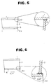
- the conventional light emitting device is constructed as above, when frit glass is applied uniformly onto each bonding surface of the spacer 3, it is necessary that the amount of frit glass discharged from the dispenser nozzle and the moving speed of the dispenser be always kept constant. However, this is difficult particularly at the corner portions, thus sometimes resulting in that the amount of frit glass applied is not uniform in some points. Consequently, as shown in Fig. 5, there may occur protrusion of frit glass, or as shown in Figs. 6 and 7, there may occur a positional deviation, or displacement, between the spacer 3 and the front panel 1 and also between the spacer and the rear panel 6 (imbalance in pressure against the panels may be another cause of such displacement).
- the openings of the shielding electrode 4 which emit electrons are influenced by static electricity of the inner side faces of the spacer 3. Since the inner side faces of the spacer 3 are positively charged, if the openings of the shielding electrode 4 approach the spacer 3 due to displacement of the rear panel 6, the openings are strongly influenced by the positive potential of the inner side faces of the spacer 3, whereby the emission of electrons is accelerated. As a result, the luminance of the corresponding fluorescent element increases. On the other hand, as the said openings go away from the spacer 3, the luminance decreases. Thus, in the interior of the light emitting device there occur variations in luminance.
- a flourescent indicator and a method of making same is known wherein a cover plate is sealed at its perimeter to a substrate or base plate.
- the cover plate is provided with an outward directed sealing flange for sealing against a sealing ledge on the substrate.
- EP-A-0 520 139 forming prior art in accordance with Article 54(3) EPC discloses that the front panel comprises a stepped portion. Furthermore the spacer comprises a stepped portion in mirror symmetry to the stepped portion when spacer and front panel a put together and sealed.
- the present invention has been accomplished for overcoming the above-mentioned problems and it is the object of the invention to prevent displacement of the bonding surfaces of the spacer with respect to the rear panel, or shielding electrode to thereby obtain a light emitting device of high accuracy free of variations, in luminance and reduce the dead space between light emitting devices A1 and A2, thereby affording a display of high resolution.
- the portion of the rear panel to be bonded to the spacer has a difference in height for fitting with the spacer to prevent displacement between the rear panel and the spacer.
- Fig. 8 is a sectional view of a light emitting device according to an embodiment of the present invention.
- the numeral 22 denotes a difference in height, or a stepped portion for fitting with the spacer 3, formed in the portion of the rear panel 6 to be bonded with the spacer 3, and the numeral 23 denotes a control electrode for a cathode extending to the exterior through the rear panel 6.
- first frit glass is applied to a bonding surface of the spacer 3 and thereafter the rear panel 6 and the spacer 3 are combined together, followed by heating. As the frit glass melts, the rear panel 6 and the spacer 3 are fitted together, whereby the displacement of the two is suppressed. As a result, there is obtained a light emitting device of high accuracy free of variations in luminance.
- the correlation between the cathodes 7 and the fluorescent elements 2 is 1 : 2, it may be 1 : 1 or 1 : n.
- the present invention is also applicable to light emitting devices based on the principle of a discharge tube or the like.
Landscapes
- Engineering & Computer Science (AREA)
- Manufacturing & Machinery (AREA)
- Cathode-Ray Tubes And Fluorescent Screens For Display (AREA)
- Vessels, Lead-In Wires, Accessory Apparatuses For Cathode-Ray Tubes (AREA)
Description
Claims (2)
- A light emitting device including:a front panel (1) on which fluorescent elements (2) are arranged in a matrix form;a rear panel (6) on which cathodes (7) are arranged in a corresponding relation to said fluorescent elements (2), said cathodes (7) emitting thermoelectrons for causing the fluorescent elements (2) to emit light; anda square frame-like spacer (3), one opening portion of said spacer being covered with said front panel (1) and the other opening portion thereof covered with said rear panel (6),wherein a stepped portion (22) for fitting with said spacer (3) is formed in a portion of said rear panel (6) to be bonded with the spacer (3).
- A method for fabricating a light emitting device including a front panel (1) on which fluorescent elements (2) are arranged in a matrix form, a rear panel (6) on which cathodes (7) are arranged in a corresponding relation to said fluorescent elements (2), said cathodes (7) emitting thermoelectrons for causing the fluorescent elements (2) to emit light, and a square frame-like spacer (3), one opening portion of said spacer (3) being covered with said front panel (1) and the other opening portion thereof covered with said rear panel (6), said method including the steps of:forming a stepped portion (22) for fitting with said spacer (3) in a surface of said rear panel (6) to be bonded with the spacer (3);applying frit glass to said spacer (3) bonding surface;combining said rear panel (6) and said spacer (3) with each other; andheating said frit glass to effect bonding between said rear panel (6) and said spacer (3).
Priority Applications (2)
| Application Number | Priority Date | Filing Date | Title |
|---|---|---|---|
| EP97122187A EP0834903A1 (en) | 1991-07-16 | 1992-03-16 | Light emitting device |
| EP97122188A EP0855732A1 (en) | 1991-07-16 | 1992-03-16 | Light emitting device |
Applications Claiming Priority (3)
| Application Number | Priority Date | Filing Date | Title |
|---|---|---|---|
| JP3174899A JP2804392B2 (en) | 1991-07-16 | 1991-07-16 | Light emitting device and manufacturing method thereof |
| JP174899/91 | 1991-07-16 | ||
| EP92104501A EP0523318B1 (en) | 1991-07-16 | 1992-03-16 | Light-emitting device |
Related Parent Applications (2)
| Application Number | Title | Priority Date | Filing Date |
|---|---|---|---|
| EP92104501.9 Division | 1992-03-16 | ||
| EP92104501A Division EP0523318B1 (en) | 1991-07-16 | 1992-03-16 | Light-emitting device |
Related Child Applications (2)
| Application Number | Title | Priority Date | Filing Date |
|---|---|---|---|
| EP97122187A Division EP0834903A1 (en) | 1991-07-16 | 1992-03-16 | Light emitting device |
| EP97122188A Division EP0855732A1 (en) | 1991-07-16 | 1992-03-16 | Light emitting device |
Publications (2)
| Publication Number | Publication Date |
|---|---|
| EP0678893A1 EP0678893A1 (en) | 1995-10-25 |
| EP0678893B1 true EP0678893B1 (en) | 1998-07-15 |
Family
ID=15986638
Family Applications (4)
| Application Number | Title | Priority Date | Filing Date |
|---|---|---|---|
| EP97122187A Withdrawn EP0834903A1 (en) | 1991-07-16 | 1992-03-16 | Light emitting device |
| EP95111009A Expired - Lifetime EP0678893B1 (en) | 1991-07-16 | 1992-03-16 | Light emitting device |
| EP92104501A Expired - Lifetime EP0523318B1 (en) | 1991-07-16 | 1992-03-16 | Light-emitting device |
| EP97122188A Withdrawn EP0855732A1 (en) | 1991-07-16 | 1992-03-16 | Light emitting device |
Family Applications Before (1)
| Application Number | Title | Priority Date | Filing Date |
|---|---|---|---|
| EP97122187A Withdrawn EP0834903A1 (en) | 1991-07-16 | 1992-03-16 | Light emitting device |
Family Applications After (2)
| Application Number | Title | Priority Date | Filing Date |
|---|---|---|---|
| EP92104501A Expired - Lifetime EP0523318B1 (en) | 1991-07-16 | 1992-03-16 | Light-emitting device |
| EP97122188A Withdrawn EP0855732A1 (en) | 1991-07-16 | 1992-03-16 | Light emitting device |
Country Status (4)
| Country | Link |
|---|---|
| US (3) | US5304083A (en) |
| EP (4) | EP0834903A1 (en) |
| JP (1) | JP2804392B2 (en) |
| DE (2) | DE69226290T2 (en) |
Families Citing this family (17)
| Publication number | Priority date | Publication date | Assignee | Title |
|---|---|---|---|---|
| JP2568633Y2 (en) * | 1993-05-27 | 1998-04-15 | 双葉電子工業株式会社 | Fluorescent tube |
| JP3426340B2 (en) * | 1994-05-30 | 2003-07-14 | ノリタケ伊勢電子株式会社 | Display tube for light source and method of manufacturing the same |
| US5629583A (en) * | 1994-07-25 | 1997-05-13 | Fed Corporation | Flat panel display assembly comprising photoformed spacer structure, and method of making the same |
| JP3624041B2 (en) * | 1995-01-06 | 2005-02-23 | キヤノン株式会社 | Image display device using conductive frit |
| US5688158A (en) * | 1995-08-24 | 1997-11-18 | Fed Corporation | Planarizing process for field emitter displays and other electron source applications |
| US5828288A (en) * | 1995-08-24 | 1998-10-27 | Fed Corporation | Pedestal edge emitter and non-linear current limiters for field emitter displays and other electron source applications |
| US5844351A (en) * | 1995-08-24 | 1998-12-01 | Fed Corporation | Field emitter device, and veil process for THR fabrication thereof |
| JP3658110B2 (en) * | 1995-11-27 | 2005-06-08 | キヤノン株式会社 | Manufacturing method and manufacturing apparatus for image display device |
| US5785569A (en) * | 1996-03-25 | 1998-07-28 | Micron Technology, Inc. | Method for manufacturing hollow spacers |
| JP3044609B2 (en) * | 1997-06-25 | 2000-05-22 | 双葉電子工業株式会社 | Display device |
| US6126505A (en) * | 1998-11-30 | 2000-10-03 | Candescent Technologies Corporation | Composite frit frame with backbone |
| AU2001234645A1 (en) * | 2000-01-21 | 2001-07-31 | Ceravision Technology Limited | Visual display |
| WO2002073579A2 (en) * | 2001-03-14 | 2002-09-19 | Telegen Corporation | Three plate structure vacuum flat panel display |
| FR2824026B1 (en) * | 2001-04-27 | 2003-07-04 | Sai Automotive Allibert Ind | STRUCTURING AERAULIC DUCT |
| JP5590935B2 (en) * | 2010-03-29 | 2014-09-17 | キヤノン株式会社 | Airtight container manufacturing method |
| CN106371254A (en) | 2016-10-28 | 2017-02-01 | 上海中航光电子有限公司 | Array substrate and display panel |
| CN114649313B (en) * | 2020-12-18 | 2025-09-09 | 富泰华工业(深圳)有限公司 | Method for manufacturing a display device |
Citations (1)
| Publication number | Priority date | Publication date | Assignee | Title |
|---|---|---|---|---|
| EP0520139A1 (en) * | 1991-06-25 | 1992-12-30 | Ise Electronics Corporation | Light-emitting device |
Family Cites Families (23)
| Publication number | Priority date | Publication date | Assignee | Title |
|---|---|---|---|---|
| US2731578A (en) * | 1951-04-30 | 1956-01-17 | Eitel Mccullough Inc | Electron tube |
| US3299305A (en) * | 1963-06-28 | 1967-01-17 | Burroughs Corp | Cathode ray circuit condition indicator tube |
| US3599027A (en) * | 1970-02-24 | 1971-08-10 | Japan Radio Co Ltd | Display discharge tube having improved display substrate and method of making same |
| US3919452A (en) * | 1973-10-23 | 1975-11-11 | Vitta Corp | Precision bonding system |
| JPS5315750A (en) * | 1976-07-28 | 1978-02-14 | Ise Electronics Corp | Vacuum display tube flit seal and method of fabricating same |
| US4259613A (en) | 1978-01-11 | 1981-03-31 | Wagner Electric Corporation | Fluorescent indicator and method of making same |
| US4302706A (en) * | 1978-06-22 | 1981-11-24 | Wagner Electric Corporation | Glass-to-glass sealing method with conductive layer |
| JPS5626337A (en) * | 1979-08-09 | 1981-03-13 | Nec Corp | Manufacture of planar display device |
| US4935583A (en) * | 1980-05-30 | 1990-06-19 | Kyle James C | Insulated conductor with ceramic-connected elements |
| US4407658A (en) * | 1981-03-02 | 1983-10-04 | Beckman Instruments, Inc. | Gas discharge display device sealing method for reducing gas contamination |
| JPS57189452A (en) * | 1981-05-19 | 1982-11-20 | Fujitsu Ltd | Color light-source tube |
| JPS57199159A (en) * | 1981-06-02 | 1982-12-07 | Toshiba Corp | Plate-like displayer |
| CA1266297A (en) * | 1983-07-30 | 1990-02-27 | Hideaki Nakagawa | Luminescent display cell |
| JPS6032240A (en) * | 1983-07-30 | 1985-02-19 | Sony Corp | Phosphor display device |
| JPH061674B2 (en) * | 1984-12-04 | 1994-01-05 | ソニー株式会社 | Fluorescent display tube |
| JPH0640474B2 (en) * | 1985-07-08 | 1994-05-25 | 伊勢電子工業株式会社 | Display tube for light source |
| JPS62147635A (en) * | 1985-12-20 | 1987-07-01 | Matsushita Electric Ind Co Ltd | display device |
| US4954885A (en) * | 1987-02-25 | 1990-09-04 | Mitsubishi Denki Kabushiki Kaisha | Filter for separating luminance and chrominance signals from composite color television signal |
| JPH01100854A (en) * | 1987-10-12 | 1989-04-19 | Mitsubishi Electric Corp | Fluorescent character display |
| US4972116A (en) * | 1988-03-15 | 1990-11-20 | Ise Electronics Corporation | Light source display tube |
| US4970430A (en) * | 1988-03-31 | 1990-11-13 | Ise Electronics Corporation | Fluorescent display apparatus |
| DE68921592T2 (en) * | 1988-12-29 | 1995-10-19 | Sony Corp | Playback device. |
| JPH04342940A (en) * | 1991-05-20 | 1992-11-30 | Futaba Corp | Vacuum envelope |
-
1991
- 1991-07-16 JP JP3174899A patent/JP2804392B2/en not_active Expired - Fee Related
-
1992
- 1992-03-12 US US07/851,462 patent/US5304083A/en not_active Expired - Fee Related
- 1992-03-16 DE DE69226290T patent/DE69226290T2/en not_active Expired - Fee Related
- 1992-03-16 DE DE69207974T patent/DE69207974T2/en not_active Expired - Fee Related
- 1992-03-16 EP EP97122187A patent/EP0834903A1/en not_active Withdrawn
- 1992-03-16 EP EP95111009A patent/EP0678893B1/en not_active Expired - Lifetime
- 1992-03-16 EP EP92104501A patent/EP0523318B1/en not_active Expired - Lifetime
- 1992-03-16 EP EP97122188A patent/EP0855732A1/en not_active Withdrawn
-
1993
- 1993-12-08 US US08/162,949 patent/US5406170A/en not_active Expired - Fee Related
-
1996
- 1996-01-11 US US08/584,098 patent/US5844358A/en not_active Expired - Fee Related
Patent Citations (1)
| Publication number | Priority date | Publication date | Assignee | Title |
|---|---|---|---|---|
| EP0520139A1 (en) * | 1991-06-25 | 1992-12-30 | Ise Electronics Corporation | Light-emitting device |
Also Published As
| Publication number | Publication date |
|---|---|
| US5304083A (en) | 1994-04-19 |
| EP0523318A2 (en) | 1993-01-20 |
| DE69226290T2 (en) | 1999-02-25 |
| EP0523318B1 (en) | 1996-01-31 |
| EP0834903A1 (en) | 1998-04-08 |
| US5406170A (en) | 1995-04-11 |
| EP0678893A1 (en) | 1995-10-25 |
| DE69226290D1 (en) | 1998-08-20 |
| EP0523318A3 (en) | 1993-03-17 |
| JPH0521025A (en) | 1993-01-29 |
| DE69207974T2 (en) | 1996-09-05 |
| DE69207974D1 (en) | 1996-03-14 |
| US5844358A (en) | 1998-12-01 |
| JP2804392B2 (en) | 1998-09-24 |
| EP0855732A1 (en) | 1998-07-29 |
Similar Documents
| Publication | Publication Date | Title |
|---|---|---|
| US5874802A (en) | Cathode body, electron gun, and cathode ray tube employing a ferroelectric emitter | |
| US5576596A (en) | Optical devices such as flat-panel cathode ray tube, having raised black matrix | |
| US5304083A (en) | Method of forming a light emitting device | |
| US6129603A (en) | Low temperature glass frit sealing for thin computer displays | |
| US5899350A (en) | Hermetic container and a supporting member for the same | |
| GB2306230A (en) | Plasma addressed liquid crystal display device | |
| US4994704A (en) | Cathode ray tube and an envelope therefor | |
| EP0520139B1 (en) | Light-emitting device | |
| US5940163A (en) | Photon coupled color flat panel display and method of manufacture | |
| US6366269B1 (en) | Method and apparatus for spacing apart panels in flat panel displays | |
| US20020167265A1 (en) | Display device | |
| KR20020087495A (en) | Display panel and production method therefor | |
| US5886463A (en) | Thin-type display device with one-piece rear wall | |
| JPH05266832A (en) | Display element | |
| US7233103B2 (en) | Image display device | |
| US5473217A (en) | Cathode-ray tube having multiple gun and deflection assemblies in an evacuated chamber | |
| KR0171993B1 (en) | Method for connecting glass tube to base in plate display | |
| JPH0745215A (en) | Cathode-ray tube | |
| EP1833074B1 (en) | Image display device | |
| KR100446226B1 (en) | Flat Panel Display | |
| KR19990012119A (en) | Field emission display device and assembly method thereof | |
| US5798607A (en) | Phosphor search including a non-pigmented phosphor and RGB phosphor elements for a CRT | |
| KR0172900B1 (en) | Shadow mask fixing device of flat CRT | |
| JPH04357653A (en) | Flat panel image display device and its manufacturing method | |
| EP1432003A1 (en) | Cathode ray tube (CRT) including a shadow mask with a partially etched mask border and skirt |
Legal Events
| Date | Code | Title | Description |
|---|---|---|---|
| PUAI | Public reference made under article 153(3) epc to a published international application that has entered the european phase |
Free format text: ORIGINAL CODE: 0009012 |
|
| 17P | Request for examination filed |
Effective date: 19950713 |
|
| AC | Divisional application: reference to earlier application |
Ref document number: 523318 Country of ref document: EP |
|
| AK | Designated contracting states |
Kind code of ref document: A1 Designated state(s): CH DE FR GB LI |
|
| 17Q | First examination report despatched |
Effective date: 19960708 |
|
| GRAG | Despatch of communication of intention to grant |
Free format text: ORIGINAL CODE: EPIDOS AGRA |
|
| GRAG | Despatch of communication of intention to grant |
Free format text: ORIGINAL CODE: EPIDOS AGRA |
|
| GRAH | Despatch of communication of intention to grant a patent |
Free format text: ORIGINAL CODE: EPIDOS IGRA |
|
| GRAH | Despatch of communication of intention to grant a patent |
Free format text: ORIGINAL CODE: EPIDOS IGRA |
|
| GRAA | (expected) grant |
Free format text: ORIGINAL CODE: 0009210 |
|
| AC | Divisional application: reference to earlier application |
Ref document number: 523318 Country of ref document: EP |
|
| AK | Designated contracting states |
Kind code of ref document: B1 Designated state(s): CH DE FR GB LI |
|
| REG | Reference to a national code |
Ref country code: CH Ref legal event code: EP |
|
| REF | Corresponds to: |
Ref document number: 69226290 Country of ref document: DE Date of ref document: 19980820 |
|
| REG | Reference to a national code |
Ref country code: CH Ref legal event code: NV Representative=s name: BOVARD AG PATENTANWAELTE |
|
| ET | Fr: translation filed | ||
| REG | Reference to a national code |
Ref country code: GB Ref legal event code: 727 |
|
| REG | Reference to a national code |
Ref country code: GB Ref legal event code: 727A |
|
| PLBE | No opposition filed within time limit |
Free format text: ORIGINAL CODE: 0009261 |
|
| STAA | Information on the status of an ep patent application or granted ep patent |
Free format text: STATUS: NO OPPOSITION FILED WITHIN TIME LIMIT |
|
| REG | Reference to a national code |
Ref country code: GB Ref legal event code: 727B |
|
| REG | Reference to a national code |
Ref country code: GB Ref legal event code: SP |
|
| 26N | No opposition filed | ||
| REG | Reference to a national code |
Ref country code: GB Ref legal event code: IF02 |
|
| PGFP | Annual fee paid to national office [announced via postgrant information from national office to epo] |
Ref country code: FR Payment date: 20020312 Year of fee payment: 11 |
|
| PGFP | Annual fee paid to national office [announced via postgrant information from national office to epo] |
Ref country code: DE Payment date: 20020327 Year of fee payment: 11 |
|
| PGFP | Annual fee paid to national office [announced via postgrant information from national office to epo] |
Ref country code: CH Payment date: 20020328 Year of fee payment: 11 |
|
| PG25 | Lapsed in a contracting state [announced via postgrant information from national office to epo] |
Ref country code: LI Free format text: LAPSE BECAUSE OF NON-PAYMENT OF DUE FEES Effective date: 20030331 Ref country code: CH Free format text: LAPSE BECAUSE OF NON-PAYMENT OF DUE FEES Effective date: 20030331 |
|
| PG25 | Lapsed in a contracting state [announced via postgrant information from national office to epo] |
Ref country code: DE Free format text: LAPSE BECAUSE OF NON-PAYMENT OF DUE FEES Effective date: 20031001 |
|
| REG | Reference to a national code |
Ref country code: CH Ref legal event code: PL |
|
| PG25 | Lapsed in a contracting state [announced via postgrant information from national office to epo] |
Ref country code: FR Free format text: LAPSE BECAUSE OF NON-PAYMENT OF DUE FEES Effective date: 20031127 |
|
| REG | Reference to a national code |
Ref country code: FR Ref legal event code: ST |
|
| PGFP | Annual fee paid to national office [announced via postgrant information from national office to epo] |
Ref country code: GB Payment date: 20050316 Year of fee payment: 14 |
|
| PG25 | Lapsed in a contracting state [announced via postgrant information from national office to epo] |
Ref country code: GB Free format text: LAPSE BECAUSE OF NON-PAYMENT OF DUE FEES Effective date: 20060316 |
|
| GBPC | Gb: european patent ceased through non-payment of renewal fee |
Effective date: 20060316 |