EP0678751A1 - Detektorvorrichtung für micht-flüchtige Änderungen einer Versorgungsspannung - Google Patents
Detektorvorrichtung für micht-flüchtige Änderungen einer Versorgungsspannung Download PDFInfo
- Publication number
- EP0678751A1 EP0678751A1 EP95400862A EP95400862A EP0678751A1 EP 0678751 A1 EP0678751 A1 EP 0678751A1 EP 95400862 A EP95400862 A EP 95400862A EP 95400862 A EP95400862 A EP 95400862A EP 0678751 A1 EP0678751 A1 EP 0678751A1
- Authority
- EP
- European Patent Office
- Prior art keywords
- voltage
- supply voltage
- value
- circuit
- conduction
- Prior art date
- Legal status (The legal status is an assumption and is not a legal conclusion. Google has not performed a legal analysis and makes no representation as to the accuracy of the status listed.)
- Granted
Links
Images

Classifications
-
- G—PHYSICS
- G01—MEASURING; TESTING
- G01R—MEASURING ELECTRIC VARIABLES; MEASURING MAGNETIC VARIABLES
- G01R19/00—Arrangements for measuring currents or voltages or for indicating presence or sign thereof
- G01R19/165—Indicating that current or voltage is either above or below a predetermined value or within or outside a predetermined range of values
- G01R19/16533—Indicating that current or voltage is either above or below a predetermined value or within or outside a predetermined range of values characterised by the application
- G01R19/16538—Indicating that current or voltage is either above or below a predetermined value or within or outside a predetermined range of values characterised by the application in AC or DC supplies
Definitions
- the present invention relates to a device for detecting the non-transient variation of an electrical supply voltage.
- a person skilled in the art knows how to compare the value of a voltage to be monitored, such as the value of the voltage of a storage battery, with a threshold value, so as to generate a signal during crossing of this threshold value by the voltage to be monitored.
- this operating mode from a comparator allows at most to detect only the crossing of the threshold value, without giving information relative to the transitory nature or not of this crossing, except for providing circuits for filtering transient disturbances. of this voltage to monitor.
- the triggering of these comparators involves triggering either by higher values or by lower values, the use of monitoring devices which can be used both at the initialization or start-up of these devices and at the end of their duration. life of their supply accumulator battery in fact involving the doubling of these devices by paralleling this type of comparators, one triggering on overshoot by higher values, the other by values lower.
- the object of the present invention is to remedy the aforementioned drawbacks of the devices of the prior art by the use of a device for detecting the non-transient variation of a supply voltage making it possible to deliver a detected signal of constant value. , as long as the supply voltage is greater than a determined threshold value, and a detected signal whose value is equal to that of the supply voltage, as long as the latter is less than said threshold value.
- Another object of the present invention is the implementation of a device for detecting the non-transient variation of an electrical supply voltage making it possible to control and monitor the level of the supply voltage of electronic, micro-electronic or computer devices, at the cost of very low consumption of electrical energy from this power source.
- the device for detecting the non-transient variation of a supply voltage relative to a reference voltage is remarkable in that it comprises a detector circuit with asymmetric threshold of a voltage variation comprising a reference input connected to the reference voltage, and a detection input supplied by the supply voltage via a first potentiometric divider.
- the threshold detector circuit makes it possible to deliver a variable voltage from the reference voltage copying variations, with the same slope, of the supply voltage.
- a level comparator circuit is provided, this circuit comprising a negative comparison input and a positive comparison input.
- the negative comparison input is connected to the threshold detector circuit and receives the variable voltage and the positive comparison input is connected to the supply voltage via a second potentiometric, adjustable divider, controlled by the output of the level comparator circuit.
- the level comparator circuit generates on its output a signal whose value is equal to either the value of the supply voltage, when the latter is less than or equal to a threshold value, or to the value of the reference voltage when the supply voltage is greater than this threshold value.
- the detection device object of the invention finds application in the electronic or micro-electronic industry for the implementation of circuits for controlling or monitoring the supply voltage of computer or micro-electronic, portable, implanted or automotive electronics.
- the device for detecting the non-transient variation of an electrical supply voltage, object of the present invention will now be described in connection with FIGS. 1 and following.
- the device object of the present invention comprises a circuit 1 detector with asymmetric threshold of a voltage variation, this circuit allowing, from the reference voltage, denoted V REF , to deliver a variable voltage, which is a copy of the variations, with the same slope, of the voltage power supply marked V CC .
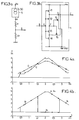
- the transfer function of the detector circuit 1 is shown in Figures 2a and 2b, which will be explained later in the description.
- the threshold detector circuit 1 comprises a reference input connected to the reference voltage V REF , and a detection input.
- the detection input is supplied by the supply voltage V DC via a first potentiometric divider.
- the first potentiometric divider as shown in FIG. 2a, delivers from the supply voltage V CC when this is subjected to variations, a signal represented, corresponding to the test point.
- a of FIG. 1 this variation being represented between the reference voltage V REF and the supply voltage V CC with a slope k1 during, for example, the powering up of the assembly of the detection device represented in FIG. 1, the first potentiometric divider device delivering to the input of the detector circuit 1 a corresponding voltage with a slope of value k'1, as shown for the test point B in FIG. 1 in dashed lines in FIG. 2a.
- the threshold detector circuit 1 makes it possible to deliver, as represented in FIG. 2a, the signal as represented at the test point C of FIG. 1, this signal corresponding to the variable voltage, with the same slope k1 as that of the variation of the supply voltage with a delay due to the asymmetry of the threshold of the detector, this delay being noted ⁇ t in FIG. 2a.
- the operation of the detection device shown in FIG. 1 is as follows: for a variation of the supply voltage V CC from a substantially stable starting voltage value, when the power is turned on at an instant t0 of l for example, starting from a zero value corresponding to the reference voltage V REF , the voltage delivered to the test point D in FIG. 1 corresponding to the positive input of the level 2 comparator circuit, changes with a slope k2 , as shown in FIG. 2a, less than the slope k1 of the variable voltage delivered by the threshold detector circuit 1.
- the output signal Vs delivered by the level 2 comparator circuit is none other than the supply voltage ion V CC , as long as the variable voltage delivered by the threshold detector circuit 1 is less than the signal delivered by the second potentiometric divider at the positive comparison input of the level comparator circuit 2.
- the level 2 comparator circuit causes switching and the output voltage Vs previously equal to the aforementioned variable voltage and delivers, on switching, a constant voltage equal to the reference voltage V REF .
- FIG. 2a a variation of the supply voltage is also shown from the maximum value V CCmax with an opposite slope -k1.
- the value of the voltage at the test point D is for example equal to V DC , fixed by the switched value of the second potentiometer.
- the value of the voltage at the test point D is for example equal to V D , fixed by the unswitched value of the second potentiometer.
- variable voltage at point C evolves with the same slope -k1 from the initial value V C.
- the voltage at point D furthermore changes from the initial value V D or V DC whether or not there is a return to the initial value, with a slope -k2 respectively -k3 as a function of the non-switched or switched value of the second potentiometric divider.
- V threshold1 and V threshold2 are different, since they depend on the initial values V D , V DC .
- the first potentiometric divider can comprise, connected in cascade between the supply voltage V CC and the reference voltage V REF , a circuit 3 of current type constant making it possible to attenuate the transient variations of the supply voltage V CC at the input of the level comparator circuit 1.
- this circuit 3 can be constituted by a current generator, which, due to the current imposed by the latter, substantially imposes on the test point A of FIG. 1 a DC voltage substantially equal to the supply voltage V CC at this point.
- the second potentiometric divider it is indicated that it can be formed by, successively connected between the supply voltage V CC and the reference voltage V REF , a programmable adjustable impedance Z3, a resistor Z4 and a resistor Z5, the impedances or resistors Z3 to Z5 being connected between the supply voltage and the reference voltage V REF , the common point between the resistance Z4 and the resistance Z5 being connected to the positive comparison input of the level comparator circuit 2.
- the impedance Z3 When switching via the output voltage Vs, it is indicated that the impedance Z3 is brought to a value greater than the abovementioned initial value, this value of Z3 being chosen so that, after switching by the intermediate of the output voltage Vs, the voltage at the test point D delivered by the second potentiometric divider is either lower than the voltage delivered on the negative comparison input of the level 2 comparator circuit, or at the intersection value of the curves of slope k1 and k2 in Figure 2.
- FIG. 2b shows the corresponding timing diagram of the output voltage Vs delivered by the output of the level 2 comparator.
- threshold detector circuit 1 A more detailed description of the threshold detector circuit 1 will now be given in conjunction with FIG. 3b.
- the threshold detector circuit 1 can advantageously comprise a first, a second, a third and a fourth MOS transistor, referenced 11, 12, 13, 14 respectively, connected in series between the voltage d V DC supply and the reference voltage V REF .
- the first and second MOS transistors 11 and 12 are of the same first type of conduction, type P in the case of the representation of FIG. 3b, and the third and fourth MOS transistors 13 and 14 are of a second type of conduction , opposite to the first type, and therefore of type N in the case of the representation of FIG. 3b.
- the first divider bridge as shown for example in FIG. 3a, is then connected in parallel from the common point between the impedances Z1 and Z2 to the gate of the first, second, third and fourth transistors MOS 11, 12, 13 and 14.
- a fifth MOS transistor, denoted 15, of the same type of conduction as the first type of conduction, of type P, is provided, the gate electrode of the fifth MOS transistor 15 being connected to the common point between the second and the third MOS transistor 12, 13 previously mentioned.
- the source and drain electrodes of the fifth MOS transistor 15 are connected between the common point of the first and of the second MOS transistor 11, 12 and the reference voltage V REF .
- the fifth MOS transistor 15 has a resistance much greater than that of the first MOS transistor 11 in a ratio of approximately 1000.
- the drain and source electrodes of the sixth MOS transistor 16 are connected between the supply voltage V CC and the common point between the third and the fourth MOS transistor 13, 14 previously mentioned.
- test points E correspond respectively to the test points B in FIG. 1, at the point in common between the second and the third MOS transistor 12, 13, that is to say say to the gate of the fifth MOS transistor 15, and to the common point between the first and the second MOS transistor 11, 12 as well as at the test points C of FIG. 1, that is to say at the output of the detector circuit at threshold 1 in Figure 1.
- test points E and F are first of all at zero. During the rise of the supply voltage to the value V CCmax with the slope k1, the voltage at the test point G, that is to say at the output of the threshold detector circuit, remains at the value of the voltage V REF . It is the same for the test point F due to the absence of conduction of the first, second, third and fourth MOS transistors 11 to 14.
- variable voltage delivered by the threshold detector circuit 1 also follows the slope of this variable supply voltage due to the value of the above impedances.
- the circuit for attenuation of the transient variations of the supply voltage V CC , the circuit 3, and more specifically the current generator 30, can be produced by CMOS technology, which of course allows, from an embodiment as shown in FIG. 3b for the threshold detector circuit 1 and for the level 2 comparator circuit, to envisage the realization of the detection device object of the present invention in the form of an integrated circuit.
- the impedances Z1 to Z5 can also be produced by means of MOS type transistors, which can allow the production of resistances of good precision.
- adjustable impedance Z3 With regard more particularly to the adjustable impedance Z3, it is indicated that this can be achieved in the form of programmable impedances by means of MOS circuits so as to also allow the integration of the assembly.
- the final values V D, V DC and V threshold 1 threshold, V threshold2, V seuil2c can thus be adjusted.
- the detection device which is the subject of the present invention, can advantageously include a control circuit 4 making it possible to deliver a commissioning or blocking signal, this signal being denoted SCFB on Figure 1 above.
- This start-up or blocking signal makes it possible, for example, to ensure the commissioning or blocking of the current generator 3 and of the level comparator 2, which makes it possible to control the operation or the stopping of the whole of the detection device by blocking or operating the threshold detector 1, level 2 comparator and current generator 3 circuits.
- control circuit 4 can simply deliver a signal blocking or authorizing the supply of the filtering circuit 3 and the level comparator circuit 2, for example.
- control circuit 4 can deliver a periodic signal, which makes it possible to carry out a sampled command of the operation of the device, in order to obtain a reduction in the overall energy consumption of the device shown in FIG. 1.
- sampling period and duration are programmable and modular according to the application considered.
- the sampling period can be fixed for example at a value of ten minutes , the sampling time itself being for example a few hundred ms.
- the detection device object of the present invention is applied to the control and monitoring of the supply voltage of a motor vehicle for example, the sampling period can be extended to a much greater duration , one to several hours for example.
- the sampling period can be reduced if necessary to a few minutes in order to ensure constant monitoring of the supply voltage of these simulators.
- Figures 4a and 4b show the shape of the voltage variations at the test point C and D of Figure 1 respectively of a variable supply voltage and the corresponding output voltage Vs.
Landscapes
- Engineering & Computer Science (AREA)
- Power Engineering (AREA)
- Physics & Mathematics (AREA)
- General Physics & Mathematics (AREA)
- Measurement Of Current Or Voltage (AREA)
Applications Claiming Priority (2)
| Application Number | Priority Date | Filing Date | Title |
|---|---|---|---|
| FR9404875A FR2719123B1 (fr) | 1994-04-22 | 1994-04-22 | Dispositif de détection de la variation non transitoire d'une tension d'alimentation. |
| FR9404875 | 1994-04-22 |
Publications (2)
| Publication Number | Publication Date |
|---|---|
| EP0678751A1 true EP0678751A1 (de) | 1995-10-25 |
| EP0678751B1 EP0678751B1 (de) | 2002-09-18 |
Family
ID=9462426
Family Applications (1)
| Application Number | Title | Priority Date | Filing Date |
|---|---|---|---|
| EP19950400862 Expired - Lifetime EP0678751B1 (de) | 1994-04-22 | 1995-04-18 | Detektorvorrichtung für Änderungen einer Versorgungsspannung |
Country Status (3)
| Country | Link |
|---|---|
| EP (1) | EP0678751B1 (de) |
| DE (1) | DE69528209T2 (de) |
| FR (1) | FR2719123B1 (de) |
Cited By (3)
| Publication number | Priority date | Publication date | Assignee | Title |
|---|---|---|---|---|
| EP0902294A1 (de) * | 1997-09-09 | 1999-03-17 | Texas Instruments Deutschland Gmbh | Schaltungsanordnung zur Spannungsüberwachung |
| EP3425757A1 (de) * | 2017-07-07 | 2019-01-09 | Stmicroelectronics (Rousset) Sas | Schutzschaltkreis eines leistungsschalters |
| CN113419102A (zh) * | 2021-06-26 | 2021-09-21 | 广州金升阳科技有限公司 | 一种波峰检测电路及其应用 |
Families Citing this family (2)
| Publication number | Priority date | Publication date | Assignee | Title |
|---|---|---|---|---|
| US7496460B2 (en) | 2006-09-06 | 2009-02-24 | Eastway Fair Company Limited | Energy source monitoring and control system for power tools |
| FR3037148B1 (fr) | 2015-06-08 | 2018-08-17 | Stmicroelectronics (Rousset) Sas | Mesure de variations d'une tension d'alimentation |
Citations (2)
| Publication number | Priority date | Publication date | Assignee | Title |
|---|---|---|---|---|
| DE3935577A1 (de) * | 1989-10-25 | 1991-05-02 | Siemens Ag | Betriebsspannungs-ueberwachungsschaltung |
| WO1993006492A1 (de) * | 1991-09-20 | 1993-04-01 | Braun Aktiengesellschaft | Schaltungsanordnung zur erfassung einer spannung |
-
1994
- 1994-04-22 FR FR9404875A patent/FR2719123B1/fr not_active Expired - Fee Related
-
1995
- 1995-04-18 DE DE1995628209 patent/DE69528209T2/de not_active Expired - Lifetime
- 1995-04-18 EP EP19950400862 patent/EP0678751B1/de not_active Expired - Lifetime
Patent Citations (2)
| Publication number | Priority date | Publication date | Assignee | Title |
|---|---|---|---|---|
| DE3935577A1 (de) * | 1989-10-25 | 1991-05-02 | Siemens Ag | Betriebsspannungs-ueberwachungsschaltung |
| WO1993006492A1 (de) * | 1991-09-20 | 1993-04-01 | Braun Aktiengesellschaft | Schaltungsanordnung zur erfassung einer spannung |
Non-Patent Citations (3)
| Title |
|---|
| ANONYMUS: "BULK SUPPLY SUPERVISORY CIRCUIT", RESEARCH DISCLOSURE, no. 325, EMSWORTH GB, pages 356 * |
| ANONYMUS: "CMOS POWER ON DETECTION CIRCUIT", RESEARCH DISCLOSURE, no. 335, EMSWORTH GB, pages 224 - 225 * |
| SCHALDACH: "DESIGN AND RELIABILITY CONSIDERATIONS IN IMPLANTS", PROC. ANNUAL INTERNAT. CONF. IEEE ENGINEERING IN MEDICINE AND BIOLOGY SOCIETY. PART 3/3 COMPUTERS AND SIGNAL PROCESSING IN MEDICINE, 7 November 1988 (1988-11-07), NEW ORLEANS, LOUISIANA, USA, pages 1235 - 1238 * |
Cited By (6)
| Publication number | Priority date | Publication date | Assignee | Title |
|---|---|---|---|---|
| EP0902294A1 (de) * | 1997-09-09 | 1999-03-17 | Texas Instruments Deutschland Gmbh | Schaltungsanordnung zur Spannungsüberwachung |
| EP3425757A1 (de) * | 2017-07-07 | 2019-01-09 | Stmicroelectronics (Rousset) Sas | Schutzschaltkreis eines leistungsschalters |
| FR3068836A1 (fr) * | 2017-07-07 | 2019-01-11 | Stmicroelectronics (Rousset) Sas | Circuit de protection d'un commutateur de puissance |
| US11381233B2 (en) | 2017-07-07 | 2022-07-05 | Stmicroelectronics (Rousset) Sas | Circuit for protecting a power switch |
| CN113419102A (zh) * | 2021-06-26 | 2021-09-21 | 广州金升阳科技有限公司 | 一种波峰检测电路及其应用 |
| CN113419102B (zh) * | 2021-06-26 | 2022-09-13 | 广州金升阳科技有限公司 | 一种波峰检测电路及其应用 |
Also Published As
| Publication number | Publication date |
|---|---|
| DE69528209T2 (de) | 2003-08-07 |
| DE69528209D1 (de) | 2002-10-24 |
| EP0678751B1 (de) | 2002-09-18 |
| FR2719123A1 (fr) | 1995-10-27 |
| FR2719123B1 (fr) | 1996-06-28 |
Similar Documents
| Publication | Publication Date | Title |
|---|---|---|
| EP0261118B1 (de) | Energieversorgung für reifenüberwachungsanlage | |
| EP0285478B1 (de) | Konvertierschaltung von analogen auf digitale Signale | |
| EP0110775B1 (de) | Regulierungseinrichtung mit kleiner Verlustspannung | |
| EP0190961B1 (de) | Gleichstromversorgung mit verstellbarem Arbeitspunkt | |
| EP1685622B1 (de) | Gleichgewichts-ladeverfahren für eine lithiumionen- oder lithiumpolymerbatterie | |
| FR2760163A1 (fr) | Appareil de telecommunication muni d'un dispositif de reconnaissance de peripheriques | |
| FR2634293A2 (fr) | Systeme de regulation du point de fonctionnement d'une alimentation a courant continu en zone de caracteristique generateur de tension ou de courant imposee | |
| FR2756984A1 (fr) | Alimentation de secours destinee a suppleer provisoirement a une carence d'une source d'alimentation principale | |
| CA2315896C (fr) | Circuit electronique de surveillance de tension electrique | |
| WO2021063725A1 (fr) | Procédé d'estimation de la résistance d'isolement d'un circuit haute tension d'un véhicule automobile électrique ou hybride | |
| EP0678751B1 (de) | Detektorvorrichtung für Änderungen einer Versorgungsspannung | |
| EP0809342B1 (de) | Anordnung zur Regelung der Ladung einer modularen Einheit von elektrochemischen Zellen, die in Reihe geschaltet sind und entsprechendes Modul zur Messung der Zellen | |
| EP0014149B1 (de) | Referenzspannungsgenerator und dabei angewendete Schaltung zur Messung der Schwellspannung eines MOS-Transistors | |
| EP0544589A1 (de) | Gerät zur Messung des realen Lastfaktors eines elektrischen Generators | |
| FR2467407A1 (fr) | Dispositif de mesure des valeurs cretes d'un phenomene non periodique a recurrence faible | |
| EP0305301B1 (de) | Signalkompressorschaltung, insbesondere für Fernsprechapparate | |
| FR2820923A1 (fr) | Alimentation asservie pour liaison serie, de type maitre esclave | |
| EP0549464A1 (de) | Gerät und Verfahren zur Messung des Ladezustandes eines elektrochemischen Generators | |
| EP0926810B1 (de) | Verbesserung für mehrphasige Fahrzeuggeneratorregler | |
| EP0617292B1 (de) | System zur ständigen Überwachung der elektrischen Leitfähigkeit eines Wechselstromnetzes | |
| EP3185389B1 (de) | Vorrichtung und elektrisches gerät zur erzeugung einer elektrischen spannung für eine informationsbearbeitungseinheit, und entsprechendes elektronisches system zur informationsbearbeitung | |
| CA1147027A (fr) | Circuit filtre passe-bas a tres basse frequence | |
| FR2611314A3 (fr) | Procede et dispositif de controle de la disponibilite d'une batterie d'accumulateurs | |
| FR2596596A1 (fr) | Procede et dispositif de transmission d'informations entre deux circuits electroniques | |
| EP0643310B1 (de) | Einrichtung zur Überwachung der Entladung einer Vielzahl in Reihe geschalteter Batterien |
Legal Events
| Date | Code | Title | Description |
|---|---|---|---|
| PUAI | Public reference made under article 153(3) epc to a published international application that has entered the european phase |
Free format text: ORIGINAL CODE: 0009012 |
|
| AK | Designated contracting states |
Kind code of ref document: A1 Designated state(s): DE GB IT NL |
|
| 17P | Request for examination filed |
Effective date: 19950927 |
|
| RAP1 | Party data changed (applicant data changed or rights of an application transferred) |
Owner name: MHS |
|
| 17Q | First examination report despatched |
Effective date: 19990712 |
|
| RAP1 | Party data changed (applicant data changed or rights of an application transferred) |
Owner name: ATMEL NANTES SA |
|
| RTI1 | Title (correction) |
Free format text: DETECTOR FOR VARIATIONS OF A SUPPLY VOLTAGE |
|
| RTI1 | Title (correction) |
Free format text: DETECTOR FOR VARIATIONS OF A SUPPLY VOLTAGE |
|
| GRAG | Despatch of communication of intention to grant |
Free format text: ORIGINAL CODE: EPIDOS AGRA |
|
| GRAG | Despatch of communication of intention to grant |
Free format text: ORIGINAL CODE: EPIDOS AGRA |
|
| GRAH | Despatch of communication of intention to grant a patent |
Free format text: ORIGINAL CODE: EPIDOS IGRA |
|
| GRAH | Despatch of communication of intention to grant a patent |
Free format text: ORIGINAL CODE: EPIDOS IGRA |
|
| GRAA | (expected) grant |
Free format text: ORIGINAL CODE: 0009210 |
|
| AK | Designated contracting states |
Kind code of ref document: B1 Designated state(s): DE GB IT NL |
|
| REG | Reference to a national code |
Ref country code: GB Ref legal event code: FG4D Free format text: NOT ENGLISH |
|
| REF | Corresponds to: |
Ref document number: 69528209 Country of ref document: DE Date of ref document: 20021024 |
|
| GBT | Gb: translation of ep patent filed (gb section 77(6)(a)/1977) |
Effective date: 20030113 |
|
| PLBE | No opposition filed within time limit |
Free format text: ORIGINAL CODE: 0009261 |
|
| STAA | Information on the status of an ep patent application or granted ep patent |
Free format text: STATUS: NO OPPOSITION FILED WITHIN TIME LIMIT |
|
| 26N | No opposition filed |
Effective date: 20030619 |
|
| PGFP | Annual fee paid to national office [announced via postgrant information from national office to epo] |
Ref country code: NL Payment date: 20090318 Year of fee payment: 15 Ref country code: IT Payment date: 20090420 Year of fee payment: 15 |
|
| PGFP | Annual fee paid to national office [announced via postgrant information from national office to epo] |
Ref country code: GB Payment date: 20090407 Year of fee payment: 15 |
|
| REG | Reference to a national code |
Ref country code: NL Ref legal event code: V1 Effective date: 20101101 |
|
| GBPC | Gb: european patent ceased through non-payment of renewal fee |
Effective date: 20100418 |
|
| PG25 | Lapsed in a contracting state [announced via postgrant information from national office to epo] |
Ref country code: NL Free format text: LAPSE BECAUSE OF NON-PAYMENT OF DUE FEES Effective date: 20101101 |
|
| PG25 | Lapsed in a contracting state [announced via postgrant information from national office to epo] |
Ref country code: GB Free format text: LAPSE BECAUSE OF NON-PAYMENT OF DUE FEES Effective date: 20100418 Ref country code: IT Free format text: LAPSE BECAUSE OF NON-PAYMENT OF DUE FEES Effective date: 20100418 |
|
| PGFP | Annual fee paid to national office [announced via postgrant information from national office to epo] |
Ref country code: DE Payment date: 20120427 Year of fee payment: 18 |
|
| REG | Reference to a national code |
Ref country code: DE Ref legal event code: R082 Ref document number: 69528209 Country of ref document: DE Representative=s name: GRUENECKER, KINKELDEY, STOCKMAIR & SCHWANHAEUS, DE |
|
| REG | Reference to a national code |
Ref country code: DE Ref legal event code: R082 Ref document number: 69528209 Country of ref document: DE Representative=s name: GRUENECKER, KINKELDEY, STOCKMAIR & SCHWANHAEUS, DE Effective date: 20131023 Ref country code: DE Ref legal event code: R081 Ref document number: 69528209 Country of ref document: DE Owner name: ATMEL CORPORATION, US Free format text: FORMER OWNER: ATMEL NANTES S.A., NANTES, FR Effective date: 20131023 |
|
| PG25 | Lapsed in a contracting state [announced via postgrant information from national office to epo] |
Ref country code: DE Free format text: LAPSE BECAUSE OF NON-PAYMENT OF DUE FEES Effective date: 20131101 |
|
| REG | Reference to a national code |
Ref country code: DE Ref legal event code: R119 Ref document number: 69528209 Country of ref document: DE Effective date: 20131101 |