EP0676799B1 - Extended drain resurf lateral DMOS devices - Google Patents
Extended drain resurf lateral DMOS devices Download PDFInfo
- Publication number
- EP0676799B1 EP0676799B1 EP95105403A EP95105403A EP0676799B1 EP 0676799 B1 EP0676799 B1 EP 0676799B1 EP 95105403 A EP95105403 A EP 95105403A EP 95105403 A EP95105403 A EP 95105403A EP 0676799 B1 EP0676799 B1 EP 0676799B1
- Authority
- EP
- European Patent Office
- Prior art keywords
- drift region
- region
- type
- oxide
- type drift
- Prior art date
- Legal status (The legal status is an assumption and is not a legal conclusion. Google has not performed a legal analysis and makes no representation as to the accuracy of the status listed.)
- Expired - Lifetime
Links
Images



Classifications
-
- H—ELECTRICITY
- H10—SEMICONDUCTOR DEVICES; ELECTRIC SOLID-STATE DEVICES NOT OTHERWISE PROVIDED FOR
- H10D—INORGANIC ELECTRIC SEMICONDUCTOR DEVICES
- H10D84/00—Integrated devices formed in or on semiconductor substrates that comprise only semiconducting layers, e.g. on Si wafers or on GaAs-on-Si wafers
-
- H—ELECTRICITY
- H10—SEMICONDUCTOR DEVICES; ELECTRIC SOLID-STATE DEVICES NOT OTHERWISE PROVIDED FOR
- H10D—INORGANIC ELECTRIC SEMICONDUCTOR DEVICES
- H10D62/00—Semiconductor bodies, or regions thereof, of devices having potential barriers
- H10D62/10—Shapes, relative sizes or dispositions of the regions of the semiconductor bodies; Shapes of the semiconductor bodies
- H10D62/13—Semiconductor regions connected to electrodes carrying current to be rectified, amplified or switched, e.g. source or drain regions
- H10D62/149—Source or drain regions of field-effect devices
- H10D62/151—Source or drain regions of field-effect devices of IGFETs
-
- H—ELECTRICITY
- H10—SEMICONDUCTOR DEVICES; ELECTRIC SOLID-STATE DEVICES NOT OTHERWISE PROVIDED FOR
- H10D—INORGANIC ELECTRIC SEMICONDUCTOR DEVICES
- H10D30/00—Field-effect transistors [FET]
- H10D30/01—Manufacture or treatment
- H10D30/021—Manufacture or treatment of FETs having insulated gates [IGFET]
- H10D30/0221—Manufacture or treatment of FETs having insulated gates [IGFET] having asymmetry in the channel direction, e.g. lateral high-voltage MISFETs having drain offset region or extended-drain MOSFETs [EDMOS]
-
- H—ELECTRICITY
- H10—SEMICONDUCTOR DEVICES; ELECTRIC SOLID-STATE DEVICES NOT OTHERWISE PROVIDED FOR
- H10D—INORGANIC ELECTRIC SEMICONDUCTOR DEVICES
- H10D30/00—Field-effect transistors [FET]
- H10D30/60—Insulated-gate field-effect transistors [IGFET]
- H10D30/601—Insulated-gate field-effect transistors [IGFET] having lightly-doped drain or source extensions, e.g. LDD IGFETs or DDD IGFETs
- H10D30/603—Insulated-gate field-effect transistors [IGFET] having lightly-doped drain or source extensions, e.g. LDD IGFETs or DDD IGFETs having asymmetry in the channel direction, e.g. lateral high-voltage MISFETs having drain offset region or extended drain IGFETs [EDMOS]
-
- H—ELECTRICITY
- H10—SEMICONDUCTOR DEVICES; ELECTRIC SOLID-STATE DEVICES NOT OTHERWISE PROVIDED FOR
- H10D—INORGANIC ELECTRIC SEMICONDUCTOR DEVICES
- H10D64/00—Electrodes of devices having potential barriers
- H10D64/20—Electrodes characterised by their shapes, relative sizes or dispositions
- H10D64/27—Electrodes not carrying the current to be rectified, amplified, oscillated or switched, e.g. gates
- H10D64/311—Gate electrodes for field-effect devices
- H10D64/411—Gate electrodes for field-effect devices for FETs
- H10D64/511—Gate electrodes for field-effect devices for FETs for IGFETs
- H10D64/514—Gate electrodes for field-effect devices for FETs for IGFETs characterised by the insulating layers
- H10D64/516—Gate electrodes for field-effect devices for FETs for IGFETs characterised by the insulating layers the thicknesses being non-uniform
-
- Y—GENERAL TAGGING OF NEW TECHNOLOGICAL DEVELOPMENTS; GENERAL TAGGING OF CROSS-SECTIONAL TECHNOLOGIES SPANNING OVER SEVERAL SECTIONS OF THE IPC; TECHNICAL SUBJECTS COVERED BY FORMER USPC CROSS-REFERENCE ART COLLECTIONS [XRACs] AND DIGESTS
- Y10—TECHNICAL SUBJECTS COVERED BY FORMER USPC
- Y10S—TECHNICAL SUBJECTS COVERED BY FORMER USPC CROSS-REFERENCE ART COLLECTIONS [XRACs] AND DIGESTS
- Y10S148/00—Metal treatment
- Y10S148/126—Power FETs
Definitions
- This invention is in the field of semiconductor integrated circuits and relates primarily to a method for making a high voltage PMOS device as defined in the precharacterizing portion of claim 1.
- Smart power devices combine high intelligence with low power dissipation. They typically have power Metal Oxide Semiconductor, MOS, Field Effect Transistors, FETs, in their output stages designed to operate at higher voltages, such as 15-80 volts as opposed to the normal Complementary Metal Oxide Semiconductor, CMOS, logic voltage of typically 5 volts or less, and logic devices incorporated on the same integrated circuit so that both a driver function and a controller function are provided in a single chip.
- CMOS Complementary Metal Oxide Semiconductor
- logic voltage typically 5 volts or less
- logic devices incorporated on the same integrated circuit so that both a driver function and a controller function are provided in a single chip.
- Many applications exist for smart power devices such as Liquid Crystal Display, LCD, displays, electro/mechanical devices, automobile electronic devices, projection TV, and even High Definition, HDTV.
- RESURF techniques are utilized in manufacturing high voltage N-channel Lateral Double Diffused MOS, HV NMOS, devices and high voltage P-channel LDMOS, HV PMOS devices.
- complicated charge pumping high voltage circuitry techniques are used for HV PMOS devices.
- the on-resistance of the HV PMOS device is relatively high.
- an HV PMOS device described in an article entitled "A Coplanar CMOS Power Switch,” IEEE J. Solid-State Circuits, vol. SC-16, pp 212-226, June 1981 uses a lightly doped pinched resistance as the drift region.
- CMOS smart power devices which is compatible with a standard 5 V CMOS technology
- the method comprises combining the existing technological layers in a modified way in order to create buffer regions and field plates as necessary.
- the p-type channel-stop implant is used for creating the lightly doped buffer region which separates the drain from the edge of the channel.
- a modified rule is employed for generating the p field-implant mask.
- EP-A-0 387 999 discloses a process for forming both low-voltage CMOS transistors and high-voltage CMOS transistors on a common integrated circuit chip which uses a common implantation and drive-in step to form both the n-type well of each PMOS transistor and the n-type drain extension well of each lightly-doped drain NMOS transistor and a separate implant and drive-in to form the p-type drain extension well of each lightly-doped drain PMOS transistor.
- EP-A-0 589 675 discloses a process which simultaneously forms different transistor structures including relatively high voltage CMOS transistors and relatively low voltage CMOS transistors, using a small number of masking steps.
- a boron segregation in a lightly doped RESURF region of a high voltage PMOS device is corrected by an implant at the edge of the field oxide of the HV PMOS device.
- This implant restores the boron concentration in the RESURF region and cuts off or isolates the shallow vertical junction that forms during the growth of the thick oxide, resulting in significantly improved operational characteristics of the HV PMOS device.
- the implant is accomplished very simply by adding a single additional mask step.
- the method of the invention comprises the steps defined in claim 1.
- Table A contains a listing of element names and reference numbers used in the drawings and the following description, while Table B provides the function, a specific embodiment and alternate examples of various elements. Tables A and B are incorporated herein and made a part of this specification.
- FIG 1 shows a cross-sectional view of an integrated circuit formed in accordance with the method of the invention containing a high voltage PMOS (HV PMOS) transistor 7.
- HV PMOS device 7 is formed in a well 40 which isolates HV PMOS device 7 from the semiconductor substrate 10.
- Substrate 10 is preferably n-type silicon with a relatively high resistivity of approximately 8-12 Ohm-cm.
- an HV PMOS device 7 obtained by the method of the invention has a p-tank 41 lying within n-well 40.
- P-tank 41 provides a RESURF drift region.
- a drift region rim 48 forms the outer edge of p-tank 41 and is adjacent to and in contact with channel region 49.
- An HV drain 42 is formed within p-tank 41.
- An HV source 44 is formed within n-well 40 and is separated from p-tank 41 by channel region 49.
- An HV field oxide 43 overlies a portion of the drift region p-tank 41.
- a gate oxide 47 overlies the channel region 49 and the drift region rim 48, and connects to HV field oxide 43.
- An HV n-well contact 45 is formed within n-well 40.
- FIG 1 also shows an optional mirror image gate and source consisting of HV source 44a formed within n-well 40 and separated from drain 42 by channel region 49a, HV gate oxide 47a overlaying channel region 49a and connecting with HV field oxide 43a, HV n-well contact 45a formed within n-well 40, and HV gate electrode 46a overlaying gate oxide 47a and field oxide 43a.
- P-tank 41 can be formed with lightly doped boron, for example. It has been found that when thick field oxide 43 is grown on silicon containing lightly doped boron regions, such as p-tank 41, boron may be segregated out of the silicon at the oxide growth boundary, such as drift region rim 48, and a region is formed at the growth boundary that has inferior semiconductor properties; this effect makes it difficult to form P-channel LDMOS high voltage RESURF devices with good operational characteristics. However, in accordance with the present invention, these deficiencies are advantageously minimized, as will be described later.
- an implant in drift region rim 48 at the edge of field oxide 43 restores the boron concentration in p-tank rim 48 and cuts off or isolates a shallow vertical junction that may be formed during the growth of thick oxide 43.
- FIG 2A-2J a preferred process for forming a transistor similar to FIG 1 is described.
- the following figures complete HV PMOS device 7 of FIG 1 as a single-sided device as opposed to the double-sided device shown in FIG 1.
- FIG 2A shows n type substrate 10 on which a layer of 1st oxide 110 is grown with a nitride layer 120 deposited on top. Nitride layer 120 is then masked and etched.
- FIG 2B shows n-type dopant 40A after implantation.
- N-type dopant 40A can be arsenic or phosphorous, for example.
- Photoresist 130B blocks the dopant 40A from undesired insertion.
- the implant occurs through oxide layer 110 and nitride layer 120.
- Dopant 40A is used to form tank 40.
- FIG 2C shows the result of a diffusion step which causes n-type dopant 40A to form HV n-well 40.
- the diffusion drives the dopants into substrate 10 to a depth of approximately 8 um.
- An n-type impurity concentration of approximately 1.5e16/cm 3 is sufficient for n-well 40.
- FIG 2D shows p-type implant 41A after being implanted.
- P-type dopant can be boron, for example.
- Photoresist 130D blocks the dopant 41A from undesired insertion.
- Dopant 41A is implanted within n-well 40.
- FIG 2E shows the result of a diffusion step that forms HV drift region p-tank 41.
- the drift region depth is limited to about 1-2 um so that when a depletion region is formed in drift region 41 in response to the application of a source to drain voltage (V ds ), the resulting field will impinge on the surface of the device and thereby reduce the voltage gradient on the surface, according to the well known operation of a RESURF device.
- a p-type impurity concentration of approximately 8.0e16/cm 3 is sufficient for drift region p-tank 41.
- FIG 2F shows field oxide 11, and HV PMOS field oxide 43 that are grown thermally on areas which are not covered with nitride 120. Boron may segregate out of p-tank 41 in the area adjacent to field oxide 43 during field oxide 43 growth. After oxide growth, nitride 120 is removed. Dummy oxide 140 is then grown over the exposed areas.
- FIG 2G shows a p-type dopant 220 after implantation.
- P-type dopant 220 may be boron, for example.
- a photoresist 130G blocks the dopant 220 from undesired insertion.
- P-type dopant 220 advantageously replaces boron that may be undesirably lost during the formation of field oxide 43.
- P-type dopant 220 may be annealed at this point, or preferably dopant 220 will be annealed in conjunction with a later diffusion, shown in FIG 2J for example.
- FIG 2H shows a partial HV gate oxide 47A which is formed by depositing oxide over the integrated circuit, patterning, and etching the oxide layer.
- the thickness of oxide 47A is selected so that the oxide added in the following step will combine to create the target thickness for an HV gate oxide 47, shown in FIG 2J.
- Partial HV gate oxide 47A may be 800 ⁇ thick, for example.
- a thin oxide layer 112 is deposited over the integrated circuit.
- Oxide layer 112 may form a gate oxide of low voltage devices not shown.
- Oxide layer 112 overlies partial gate oxide 47A.
- Oxide layer 112 may be approximately 350 ⁇ thick, for example.
- Oxide layer 112 is then patterned and etched, forming HV gate oxide 47 shown in FIG 2J.
- HV gate electrode 46 polysilicon has been deposited and etched to form HV gate electrode 46.
- HV p+ drain 42 and HV p+ source 44 are implanted.
- HV n+ n-well contact 45 is implanted. All of the drain and source elements (42, 44, and 45) can then be diffused in a single diffusion step to approximately the same depth to yield the device of FIG 1. Well known steps can then be followed to complete the integrated circuit.
- FIG'S 3A-3C illustrate benefits of the invention in more detail.
- Impurity concentration gradient lines 201a - 201h show the impurity concentration (i.e., boron) in the lightly doped drift region 41 after the oxide 43 growth, as shown in FIG 2F, is completed.
- Impurity concentration line 201a represents the higher concentration area, which is about 1.5e16/cm 3 .
- Impurity concentration line 201h represents the lower concentration boundary of the drift region 41.
- the impurity concentration has segregated out of the drift region tank 41, leaving a shallow vertical junction 230 under the field oxide 43. Shallow vertical junction 230 will degrade the performance of PMOS device 7.
- HV drift region tank rim adjustment 220 is shown.
- An additional implant of the same impurity used for the drift region tank 41 i.e., boron
- boron re-establishes the impurity concentration in drift region tank rim 48 and eliminates the shallow vertical junction 230.
- annealing the drift region tank rim adjustment 220 smooths the impurity gradient as shown by impurity gradient lines 201a - 201h and forms a preferred lateral junction 250.
- a very small isolated portion of the shallow vertical junction 230 may remain under field oxide 43, but this has little effect on the performance of PMOS device 7.
- the HV drift region p-tank rim 48 adjacent to the channel region 49 now advantageously does not have a deficiency of impurity concentration which would undesirably increase the on resistance, R ds(on) , of HV PMOS device 7.
- the invention is not limited to masked ion implantation onto field oxide to cutoff or isolate the shallow vertical junction which formed during thick field oxidation, as was described in the preferred embodiment. It can also be advantageously applied to many forms of vertical junction dopant compensation techniques which serve the purpose of counter doping for isolation in order to form a lateral junction.
- This invention can be advantageously applied to many forms of high voltage PMOS devices used in smart power devices.
- the present invention may be embodied using various topological shapes, such as a square drift region 41 or a rounded drift region 41, for example.
- Another advantage of the current invention is that a simple process that is adaptable to most CMOS fabrication processes allows the high voltage PMOS devices to be optimized independently of other types of devices on the integrated circuit so that R ds(on) of the high voltage PMOS device is minimized.
- Element Element Name 10 semiconductive substrate 40 HV n-well 41 HV drift region (p)-tank 42 HV p+ drain 43 HV PMOS field oxide 44, 44a HV p+ source 45, 45a HV n+ n-well contact region 46, 46a HV PMOS gate electrode 47 HV PMOS gate oxide 48 HV PMOS drift region rim 49 HV PMOS channel region 101 HV drain electrode 103 HV source electrode 110 1st oxide 120 nitride layer 130 photoresist pattern 140 dummy oxide 201A-201h impurity concentration gradient line 220 HV drift region p-tank adjustment 230 shallow verticle junction 250 lateral junction Element Function Specific embodiment HVPMOS rated breakdown 30 v.
- HV breakdown approx 15 - 80 v. 10 foundation for active elements 8-12 ohm-cm (n-) Si 8-12 onm-cm (p-) Si 40 localized semiconductive substrate well formed (n), approx 1.5e16/cm 3 approx 8 um deep approx 1.0e15 - 5.0 e16/cm 3 approx 4.0 - 10 um deep 41 drain depletion region to reduce the surface field formed boron (p), approx 8.0e16/cm 3 , approx 1.1 um deep approx 0.1 - 3.0 e17/cm 3 approx 1.0 - 2.5 um 42 highly conductive drain contact region formed (p+), approx 1.0e19/cm 3 , approx 0.5 um deep 43 insulate gate from drain and drift region thermal Si oxide, approx 9300 ⁇ 44 source region formed (p+), approx 1.0e19/cm 3 , approx 0.5 um deep 45 highly conductive tank contact region formed (n+), approx 1.0e19/cm
Landscapes
- Insulated Gate Type Field-Effect Transistor (AREA)
- Metal-Oxide And Bipolar Metal-Oxide Semiconductor Integrated Circuits (AREA)
Description
- This invention is in the field of semiconductor integrated circuits and relates primarily to a method for making a high voltage PMOS device as defined in the precharacterizing portion of
claim 1. - Integrated circuits with combined control and driver functions are often referred to as smart power devices. Smart power devices combine high intelligence with low power dissipation. They typically have power Metal Oxide Semiconductor, MOS, Field Effect Transistors, FETs, in their output stages designed to operate at higher voltages, such as 15-80 volts as opposed to the normal Complementary Metal Oxide Semiconductor, CMOS, logic voltage of typically 5 volts or less, and logic devices incorporated on the same integrated circuit so that both a driver function and a controller function are provided in a single chip. Many applications exist for smart power devices such as Liquid Crystal Display, LCD, displays, electro/mechanical devices, automobile electronic devices, projection TV, and even High Definition, HDTV.
- A technique for fabricating high voltage, HV, MOS devices is described in an article entitled "High Voltage Thin Layer Devices (RESURF Devices)," IEDM Proceedings, 1979, pp 238-241. This technique uses a shallow lightly doped region between the drain and channel regions of the device. This shallow lightly doped region is referred to as a drift region because of the low amount of current carriers (carriers being electrons or "holes") that are available due to the low level of impurity doping and the device is known as a Reduced Surface Field, RESURF, device.
- RESURF techniques are utilized in manufacturing high voltage N-channel Lateral Double Diffused MOS, HV NMOS, devices and high voltage P-channel LDMOS, HV PMOS devices. However, problems exist in manufacturing smart power devices containing such RESURF HV PMOS devices. Typically, complicated charge pumping high voltage circuitry techniques are used for HV PMOS devices. Typically the on-resistance of the HV PMOS device is relatively high. For example, an HV PMOS device described in an article entitled "A Coplanar CMOS Power Switch," IEEE J. Solid-State Circuits, vol. SC-16, pp 212-226, June 1981, uses a lightly doped pinched resistance as the drift region.
- A method for manufacture of CMOS smart power devices which is compatible with a standard 5 V CMOS technology is disclosed in the article "Design and Optimization of High-Voltage CMOS Devices Compatible with a Standard 5 V CMOS Technology" by Declercq M. et al. in Proceedings of the Custom Integrated Circuits Conference, San Diego, May 9, 1993, Institute of Electrical and Electronics Engineers, Pages 24.6.1 - 24.6.4, XP 000409742. The method comprises combining the existing technological layers in a modified way in order to create buffer regions and field plates as necessary. In manufacturing a PMOS device, the p-type channel-stop implant is used for creating the lightly doped buffer region which separates the drain from the edge of the channel. To this end, a modified rule is employed for generating the p field-implant mask.
- EP-A-0 387 999 discloses a process for forming both low-voltage CMOS transistors and high-voltage CMOS transistors on a common integrated circuit chip which uses a common implantation and drive-in step to form both the n-type well of each PMOS transistor and the n-type drain extension well of each lightly-doped drain NMOS transistor and a separate implant and drive-in to form the p-type drain extension well of each lightly-doped drain PMOS transistor.
- EP-A-0 589 675 discloses a process which simultaneously forms different transistor structures including relatively high voltage CMOS transistors and relatively low voltage CMOS transistors, using a small number of masking steps.
- Objects and advantages of the invention will be apparent to those of ordinary skill in the art having reference to the following figures and specification.
- In accordance with the present invention, a boron segregation in a lightly doped RESURF region of a high voltage PMOS device is corrected by an implant at the edge of the field oxide of the HV PMOS device. This implant restores the boron concentration in the RESURF region and cuts off or isolates the shallow vertical junction that forms during the growth of the thick oxide, resulting in significantly improved operational characteristics of the HV PMOS device. The implant is accomplished very simply by adding a single additional mask step. The method of the invention comprises the steps defined in
claim 1. -
- FIG 1 is a cross-sectional view of an integrated circuit illustrating an HV PMOS device formed on in accordance with the present invention,
- FIGS 2A - 2J are cross-sectional views illustrating a preferred method of constructing an HV PMOS device similar to FIG 1 in accordance with the present invention,
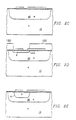
- FIG 3A is a cross-sectional view of the HV PMOS device of FIG 1 showing impurity concentration gradient lines in the HV drift region tank after field oxide growth,
- FIG 3B is a cross-sectional view of the HV PMOS device of FIG 1 showing impurity concentration gradient lines in the HV drift region tank after implanting an HV drift region tank rim adjustment, and
- FIG 3C is a sectional view of the HV PMOS device of FIG 1 showing impurity concentration gradient lines in the HV drift region tank after annealing the HV drift region tank rim adjustment.
-
- A preferred embodiment of the invention is now described. Table A contains a listing of element names and reference numbers used in the drawings and the following description, while Table B provides the function, a specific embodiment and alternate examples of various elements. Tables A and B are incorporated herein and made a part of this specification.
- FIG 1 shows a cross-sectional view of an integrated circuit formed in accordance with the method of the invention containing a high voltage PMOS (HV PMOS)
transistor 7.HV PMOS device 7 is formed in a well 40 which isolatesHV PMOS device 7 from thesemiconductor substrate 10.Substrate 10 is preferably n-type silicon with a relatively high resistivity of approximately 8-12 Ohm-cm. - In FIG 1, an
HV PMOS device 7 obtained by the method of the invention has a p-tank 41 lying within n-well 40. P-tank 41 provides a RESURF drift region. Adrift region rim 48 forms the outer edge of p-tank 41 and is adjacent to and in contact withchannel region 49. AnHV drain 42 is formed within p-tank 41. AnHV source 44 is formed within n-well 40 and is separated from p-tank 41 bychannel region 49. AnHV field oxide 43 overlies a portion of the drift region p-tank 41. Agate oxide 47 overlies thechannel region 49 and thedrift region rim 48, and connects toHV field oxide 43. An HV n-well contact 45 is formed within n-well 40. AnHV gate electrode 46overlays gate oxide 47 andfield oxide 43. FIG 1 also shows an optional mirror image gate and source consisting of HV source 44a formed within n-well 40 and separated fromdrain 42 by channel region 49a, HV gate oxide 47a overlaying channel region 49a and connecting with HV field oxide 43a, HV n-well contact 45a formed within n-well 40, and HV gate electrode 46a overlaying gate oxide 47a and field oxide 43a. - Still referring to FIG 1, P-
tank 41 can be formed with lightly doped boron, for example. It has been found that whenthick field oxide 43 is grown on silicon containing lightly doped boron regions, such as p-tank 41, boron may be segregated out of the silicon at the oxide growth boundary, such asdrift region rim 48, and a region is formed at the growth boundary that has inferior semiconductor properties; this effect makes it difficult to form P-channel LDMOS high voltage RESURF devices with good operational characteristics. However, in accordance with the present invention, these deficiencies are advantageously minimized, as will be described later. Using only one additional mask step in a standard CMOS fabrication process, an implant indrift region rim 48 at the edge offield oxide 43 restores the boron concentration in p-tank rim 48 and cuts off or isolates a shallow vertical junction that may be formed during the growth ofthick oxide 43. - Referring now to FIG 2A-2J, a preferred process for forming a transistor similar to FIG 1 is described. For simplicity, the following figures complete
HV PMOS device 7 of FIG 1 as a single-sided device as opposed to the double-sided device shown in FIG 1. - FIG 2A shows
n type substrate 10 on which a layer of1st oxide 110 is grown with anitride layer 120 deposited on top. Nitridelayer 120 is then masked and etched. - FIG 2B shows n-
type dopant 40A after implantation. N-type dopant 40A can be arsenic or phosphorous, for example. Photoresist 130B blocks thedopant 40A from undesired insertion. The implant occurs throughoxide layer 110 andnitride layer 120. Dopant 40A is used to formtank 40. - FIG 2C shows the result of a diffusion step which causes n-
type dopant 40A to form HV n-well 40. The diffusion drives the dopants intosubstrate 10 to a depth of approximately 8 um. An n-type impurity concentration of approximately 1.5e16/cm3 is sufficient for n-well 40. - FIG 2D shows p-
type implant 41A after being implanted. P-type dopant can be boron, for example.Photoresist 130D blocks thedopant 41A from undesired insertion.Dopant 41A is implanted within n-well 40. - FIG 2E shows the result of a diffusion step that forms HV drift region p-
tank 41. The drift region depth is limited to about 1-2 um so that when a depletion region is formed indrift region 41 in response to the application of a source to drain voltage (Vds), the resulting field will impinge on the surface of the device and thereby reduce the voltage gradient on the surface, according to the well known operation of a RESURF device. A p-type impurity concentration of approximately 8.0e16/cm3 is sufficient for drift region p-tank 41. - FIG 2F shows
field oxide 11, and HVPMOS field oxide 43 that are grown thermally on areas which are not covered withnitride 120. Boron may segregate out of p-tank 41 in the area adjacent to fieldoxide 43 duringfield oxide 43 growth. After oxide growth,nitride 120 is removed.Dummy oxide 140 is then grown over the exposed areas. - FIG 2G shows a p-
type dopant 220 after implantation. P-type dopant 220 may be boron, for example. Aphotoresist 130G blocks thedopant 220 from undesired insertion. According to the invention, P-type dopant 220 advantageously replaces boron that may be undesirably lost during the formation offield oxide 43. P-type dopant 220 may be annealed at this point, or preferablydopant 220 will be annealed in conjunction with a later diffusion, shown in FIG 2J for example. - FIG 2H shows a partial
HV gate oxide 47A which is formed by depositing oxide over the integrated circuit, patterning, and etching the oxide layer. The thickness ofoxide 47A is selected so that the oxide added in the following step will combine to create the target thickness for anHV gate oxide 47, shown in FIG 2J. PartialHV gate oxide 47A may be 800 Å thick, for example. - In FIG 2I, a
thin oxide layer 112 is deposited over the integrated circuit.Oxide layer 112 may form a gate oxide of low voltage devices not shown.Oxide layer 112 overliespartial gate oxide 47A.Oxide layer 112 may be approximately 350 Å thick, for example.Oxide layer 112 is then patterned and etched, formingHV gate oxide 47 shown in FIG 2J. - In FIG 2J, polysilicon has been deposited and etched to form
HV gate electrode 46. HV p+ drain 42 andHV p+ source 44 are implanted. HV n+ n-well contact 45 is implanted. All of the drain and source elements (42, 44, and 45) can then be diffused in a single diffusion step to approximately the same depth to yield the device of FIG 1. Well known steps can then be followed to complete the integrated circuit. - FIG'S 3A-3C illustrate benefits of the invention in more detail. Referring to FIG 3A, the effect of boron impurity segregation during oxide growth is shown. Impurity concentration gradient lines 201a - 201h show the impurity concentration (i.e., boron) in the lightly doped
drift region 41 after theoxide 43 growth, as shown in FIG 2F, is completed. Impurity concentration line 201a represents the higher concentration area, which is about 1.5e16/cm3. Impurity concentration line 201h represents the lower concentration boundary of thedrift region 41. In drift regiontank rim area 48, the impurity concentration has segregated out of thedrift region tank 41, leaving a shallowvertical junction 230 under thefield oxide 43. Shallowvertical junction 230 will degrade the performance ofPMOS device 7. - The invention minimizes potential device performance degradation caused by the boron segregation. Referring to FIG 3B and FIG 2G, HV drift region
tank rim adjustment 220 is shown. An additional implant of the same impurity used for the drift region tank 41 (i.e., boron) re-establishes the impurity concentration in drift region tank rim 48 and eliminates the shallowvertical junction 230. - Referring to FIG 3c, annealing the drift region
tank rim adjustment 220 smooths the impurity gradient as shown by impurity gradient lines 201a - 201h and forms a preferredlateral junction 250. A very small isolated portion of the shallowvertical junction 230 may remain underfield oxide 43, but this has little effect on the performance ofPMOS device 7. The HV drift region p-tank rim 48 adjacent to thechannel region 49 now advantageously does not have a deficiency of impurity concentration which would undesirably increase the on resistance, Rds(on), ofHV PMOS device 7. - The invention is not limited to masked ion implantation onto field oxide to cutoff or isolate the shallow vertical junction which formed during thick field oxidation, as was described in the preferred embodiment. It can also be advantageously applied to many forms of vertical junction dopant compensation techniques which serve the purpose of counter doping for isolation in order to form a lateral junction.
- This invention can be advantageously applied to many forms of high voltage PMOS devices used in smart power devices.
- The present invention may be embodied using various topological shapes, such as a
square drift region 41 or arounded drift region 41, for example. - Another advantage of the current invention is that a simple process that is adaptable to most CMOS fabrication processes allows the high voltage PMOS devices to be optimized independently of other types of devices on the integrated circuit so that Rds(on) of the high voltage PMOS device is minimized.
- While the invention has been described with respect to illustrative embodiments, this description is not intended to be construed in a limiting sense. Various other embodiments of the invention will be apparent to persons skilled in the art upon reference to this description. For example, an alternate embodiment may use either N or
P type substrate 10 since the device is isolated by well 40 in the preferred embodiment.Element Element Name 10 semiconductive substrate 40 HV n-well 41 HV drift region (p)-tank 42 HV p+ drain 43 HV PMOS field oxide 44, 44a HV p+ source 45, 45a HV n+ n-well contact region 46, 46a HV PMOS gate electrode 47 HV PMOS gate oxide 48 HV PMOS drift region rim 49 HV PMOS channel region 101 HV drain electrode 103 HV source electrode 110 1st oxide 120 nitride layer 130 photoresist pattern 140 dummy oxide 201A-201h impurity concentration gradient line 220 HV drift region p-tank adjustment 230 shallow verticle junction 250 lateral junction Element Function Specific embodiment HVPMOS rated breakdown = 30 v. Alternate examples HV breakdown = approx 15 - 80 v. 10 foundation for active elements 8-12 ohm-cm (n-) Si 8-12 onm-cm (p-) Si 40 localized semiconductive substrate well formed (n), approx 1.5e16/cm3 approx 8 um deep approx 1.0e15 - 5.0 e16/cm3 approx 4.0 - 10 um deep 41 drain depletion region to reduce the surface field formed boron (p), approx 8.0e16/cm3, approx 1.1 um deep approx 0.1 - 3.0 e17/cm3 approx 1.0 - 2.5 um 42 highly conductive drain contact region formed (p+), approx 1.0e19/cm3, approx 0.5 um deep 43 insulate gate from drain and drift region thermal Si oxide, approx 9300 Å 44 source region formed (p+), approx 1.0e19/cm3, approx 0.5 um deep 45 highly conductive tank contact region formed (n+), approx 1.0e19/cm3, approx 0.5 um deep 46 gate electrode poly Si metal, such as Al, Cu 47 insulate gate from conductive regions deposited Si oxide, aprox 1000 Å 48 rim of drift region tank 41 49 semiconductive region formed (n) 101 drain electrode poly Si a) metal, such as Al, Cu b) refractory metal silicide 103 source electrode poly Si a) metal, such as Al, Cu b) refractory metal silicide 110 etch stop for nitride, protect crystal surface thermal oxide, approx 400 Å 120 mask for field oxide deposited Si3N4, approx 1200 Å 130 mask for implants 140 protect crystal surface thermal oxide, approx 400 Å 201a-201h impurity concentration lines approx 1.0e16/cm3 per line 220 replace lost boron impurity concentration formed boron, approx 1.0e13/cm3 approx 0.5 - 1.5e13/cm3 230 undesireable side effect of thermal oxide growth boron segregation 250 lateral junction improves device performance junction between the drift region and the channel region
Claims (4)
- A method of fabricating a high voltage P-channel MOS device, comprising the steps of:a) providing a silicon substrate (10) having a major surface;b) forming an n-type doped well (40A; 40) by implantation into said silicon substrate below said major surface;c) forming a lightly doped p-type drift region (41A; 41) by implantation of boron within said n-type doped well such that a channel region is defined below said major surface in said n-type doped well;d) thermally growing a field oxide (43) at said major surface on said p-type drift region and adjacent to said channel region, which causes said boron to segregate out of said lightly doped p-type drift region at the edge of said field oxide;
characterized in thate) after step d) an additional p-type dopant is implanted into a rim region (220) of said p-type drift region to reestablish the p-type dopant concentration, and said rim region being between said channel region and the edge of said field oxide. - The method of claim 1, wherein;
the step c) of forming the lightly doped p-type drift region (41A; 41) limits the p-type drift region (41A; 41) to a depth of less than 5 µm. - The method of claim 1 or claim 2, wherein:
the step e) of implanting the additional p-type dopant into the rim region (220) of the p-type drift region uses boron as the impurity. - The method of any of the preceding claims, wherein:the step c) of forming the lightly doped p-type drift region (41A; 41) comprises implanting the p-type drift region (41A; 41) with an impurity concentration of greater than 1e15/cm3 of boron;the step d) of thermally growing the field oxide (43) at the major surface of the p-type drift region comprises growing the field oxide (43) to a thickness greater than 0.6 µm; andthe step e) of implanting the additional p-type dopant into the rim region (220) of the p-type drift region comprises implanting the rim region (220) between the channel region (49) and the edge of the field oxide (43) with an impurity concentration of greater than 0.5 e13/cm3.
Applications Claiming Priority (2)
| Application Number | Priority Date | Filing Date | Title |
|---|---|---|---|
| US22491494A | 1994-04-08 | 1994-04-08 | |
| US224914 | 1994-04-08 |
Publications (3)
| Publication Number | Publication Date |
|---|---|
| EP0676799A2 EP0676799A2 (en) | 1995-10-11 |
| EP0676799A3 EP0676799A3 (en) | 1996-06-12 |
| EP0676799B1 true EP0676799B1 (en) | 2001-12-05 |
Family
ID=22842748
Family Applications (1)
| Application Number | Title | Priority Date | Filing Date |
|---|---|---|---|
| EP95105403A Expired - Lifetime EP0676799B1 (en) | 1994-04-08 | 1995-04-10 | Extended drain resurf lateral DMOS devices |
Country Status (6)
| Country | Link |
|---|---|
| US (1) | US5512495A (en) |
| EP (1) | EP0676799B1 (en) |
| JP (1) | JPH07297294A (en) |
| KR (1) | KR100396170B1 (en) |
| DE (1) | DE69524276T2 (en) |
| TW (1) | TW305057B (en) |
Cited By (1)
| Publication number | Priority date | Publication date | Assignee | Title |
|---|---|---|---|---|
| EP2665101A1 (en) | 2012-05-14 | 2013-11-20 | austriamicrosystems AG | Method of producing a high-voltage LDMOS transistor |
Families Citing this family (27)
| Publication number | Priority date | Publication date | Assignee | Title |
|---|---|---|---|---|
| TW366543B (en) * | 1996-12-23 | 1999-08-11 | Nxp Bv | Semiconductor device |
| KR100249505B1 (en) * | 1997-10-28 | 2000-03-15 | 정선종 | Fabrication method of laterally double diffused mosfets |
| KR100300069B1 (en) | 1999-05-10 | 2001-09-26 | 김영환 | Semiconductor device and fabrication method of thereof |
| JP2001015741A (en) * | 1999-06-30 | 2001-01-19 | Toshiba Corp | Field effect transistor |
| EP1115158A1 (en) * | 2000-01-05 | 2001-07-11 | Mitsubishi Denki Kabushiki Kaisha | Soi-misfet |
| GB2374456A (en) * | 2000-12-09 | 2002-10-16 | Esm Ltd | High-voltage metal oxide semiconductor device and method of forming the device |
| US6468870B1 (en) * | 2000-12-26 | 2002-10-22 | Taiwan Semiconductor Manufacturing Company | Method of fabricating a LDMOS transistor |
| US6501139B1 (en) * | 2001-03-30 | 2002-12-31 | Matrix Semiconductor, Inc. | High-voltage transistor and fabrication process |
| KR100867574B1 (en) * | 2002-05-09 | 2008-11-10 | 페어차일드코리아반도체 주식회사 | High voltage device and manufacturing method thereof |
| KR100519642B1 (en) * | 2003-12-31 | 2005-10-07 | 동부아남반도체 주식회사 | Method for fabricating semiconductor device |
| DE102004009521B4 (en) * | 2004-02-27 | 2020-06-10 | Austriamicrosystems Ag | High-voltage PMOS transistor, mask for manufacturing a tub and method for manufacturing a high-voltage PMOS transistor |
| DE102004038369B4 (en) * | 2004-08-06 | 2018-04-05 | Austriamicrosystems Ag | High-voltage NMOS transistor and manufacturing process |
| JP4959931B2 (en) * | 2004-09-29 | 2012-06-27 | オンセミコンダクター・トレーディング・リミテッド | Manufacturing method of semiconductor device |
| KR100614806B1 (en) * | 2004-10-27 | 2006-08-22 | 삼성전자주식회사 | High breakdown voltage transistor and manufacturing method thereof |
| US7045830B1 (en) | 2004-12-07 | 2006-05-16 | Fairchild Semiconductor Corporation | High-voltage diodes formed in advanced power integrated circuit devices |
| US20060148103A1 (en) * | 2004-12-30 | 2006-07-06 | Yin-Peng Chen | Highly sensitive biological assays |
| US20060220170A1 (en) * | 2005-03-31 | 2006-10-05 | Chih-Feng Huang | High-voltage field effect transistor having isolation structure |
| US8174071B2 (en) * | 2008-05-02 | 2012-05-08 | Taiwan Semiconductor Manufacturing Co., Ltd. | High voltage LDMOS transistor |
| EP2244299A1 (en) * | 2009-04-22 | 2010-10-27 | STMicroelectronics S.r.l. | MOS transistor for power applications and corresponding integrated circuit and manufacturing method |
| EP2402998B1 (en) * | 2010-07-01 | 2020-04-08 | ams AG | Method of producing a p-channel LDMOS transistor |
| US8664720B2 (en) | 2010-08-25 | 2014-03-04 | Infineon Technologies Ag | High voltage semiconductor devices |
| US8754469B2 (en) * | 2010-10-26 | 2014-06-17 | Texas Instruments Incorporated | Hybrid active-field gap extended drain MOS transistor |
| CN104167360B (en) | 2013-05-16 | 2017-05-31 | 无锡华润上华半导体有限公司 | Transverse diffusion metal oxide semiconductor device and its manufacture method |
| CN105720099A (en) * | 2014-12-02 | 2016-06-29 | 无锡华润上华半导体有限公司 | N-type lateral double-diffused metal oxide semiconductor field effect transistor |
| US10566200B2 (en) * | 2018-04-03 | 2020-02-18 | Texas Instruments Incorporated | Method of fabricating transistors, including ambient oxidizing after etchings into barrier layers and anti-reflecting coatings |
| TWI656642B (en) * | 2018-05-08 | 2019-04-11 | Richtek Technology Corporation | Lateral double-diffused metal oxide semiconductor device and method of manufacturing same |
| CN113380787B (en) * | 2021-08-13 | 2022-02-25 | 上海维安半导体有限公司 | Bidirectional transient voltage suppression device and preparation method thereof |
Family Cites Families (17)
| Publication number | Priority date | Publication date | Assignee | Title |
|---|---|---|---|---|
| NL8203870A (en) * | 1982-10-06 | 1984-05-01 | Philips Nv | SEMICONDUCTOR DEVICE. |
| JPH07105434B2 (en) * | 1985-08-12 | 1995-11-13 | 松下電子工業株式会社 | Method for manufacturing semiconductor device |
| JPH077795B2 (en) * | 1985-12-03 | 1995-01-30 | 株式会社東芝 | Method for manufacturing semiconductor device |
| US5264719A (en) * | 1986-01-07 | 1993-11-23 | Harris Corporation | High voltage lateral semiconductor device |
| US4987093A (en) * | 1987-04-15 | 1991-01-22 | Texas Instruments Incorporated | Through-field implant isolated devices and method |
| US4984196A (en) * | 1988-05-25 | 1991-01-08 | Texas Instruments, Incorporated | High performance bipolar differential sense amplifier in a BiCMOS SRAM |
| US5156989A (en) * | 1988-11-08 | 1992-10-20 | Siliconix, Incorporated | Complementary, isolated DMOS IC technology |
| JPH02226743A (en) * | 1989-02-28 | 1990-09-10 | Mitsubishi Electric Corp | Semiconductor device and manufacture thereof |
| US5047358A (en) * | 1989-03-17 | 1991-09-10 | Delco Electronics Corporation | Process for forming high and low voltage CMOS transistors on a single integrated circuit chip |
| JP2504573B2 (en) * | 1989-08-08 | 1996-06-05 | 株式会社東芝 | Semiconductor device and manufacturing method thereof |
| US5013671A (en) * | 1990-06-20 | 1991-05-07 | Texas Instruments Incorporated | Process for reduced emitter-base capacitance in bipolar transistor |
| DE69225552T2 (en) * | 1991-10-15 | 1999-01-07 | Texas Instruments Inc., Dallas, Tex. | Lateral double-diffused MOS transistor and method for its production |
| US5306652A (en) * | 1991-12-30 | 1994-04-26 | Texas Instruments Incorporated | Lateral double diffused insulated gate field effect transistor fabrication process |
| US5322804A (en) * | 1992-05-12 | 1994-06-21 | Harris Corporation | Integration of high voltage lateral MOS devices in low voltage CMOS architecture using CMOS-compatible process steps |
| US5346835A (en) * | 1992-07-06 | 1994-09-13 | Texas Instruments Incorporated | Triple diffused lateral resurf insulated gate field effect transistor compatible with process and method |
| US5374569A (en) * | 1992-09-21 | 1994-12-20 | Siliconix Incorporated | Method for forming a BiCDMOS |
| US5328859A (en) * | 1993-01-04 | 1994-07-12 | Xerox Corporation | Method of making high voltage PNP bipolar transistor in CMOS |
-
1995
- 1995-02-16 US US08/390,269 patent/US5512495A/en not_active Expired - Lifetime
- 1995-04-08 KR KR1019950008215A patent/KR100396170B1/en not_active Expired - Lifetime
- 1995-04-10 DE DE69524276T patent/DE69524276T2/en not_active Expired - Fee Related
- 1995-04-10 EP EP95105403A patent/EP0676799B1/en not_active Expired - Lifetime
- 1995-04-10 JP JP7120339A patent/JPH07297294A/en active Pending
- 1995-06-09 TW TW084105846A patent/TW305057B/zh not_active IP Right Cessation
Cited By (2)
| Publication number | Priority date | Publication date | Assignee | Title |
|---|---|---|---|---|
| EP2665101A1 (en) | 2012-05-14 | 2013-11-20 | austriamicrosystems AG | Method of producing a high-voltage LDMOS transistor |
| WO2013171012A1 (en) | 2012-05-14 | 2013-11-21 | Ams Ag | Method of producing a high-voltage ldmos transistor |
Also Published As
| Publication number | Publication date |
|---|---|
| DE69524276T2 (en) | 2002-08-08 |
| US5512495A (en) | 1996-04-30 |
| KR100396170B1 (en) | 2003-11-14 |
| JPH07297294A (en) | 1995-11-10 |
| DE69524276D1 (en) | 2002-01-17 |
| KR950034761A (en) | 1995-12-28 |
| EP0676799A3 (en) | 1996-06-12 |
| EP0676799A2 (en) | 1995-10-11 |
| TW305057B (en) | 1997-05-11 |
Similar Documents
| Publication | Publication Date | Title |
|---|---|---|
| EP0676799B1 (en) | Extended drain resurf lateral DMOS devices | |
| US5585660A (en) | Extended drain resurf lateral DMOS devices | |
| EP0677876B1 (en) | High and low voltage CMOS device and method of fabrication | |
| US6160290A (en) | Reduced surface field device having an extended field plate and method for forming the same | |
| EP0476380B1 (en) | Self-aligned bipolar transistor structure and fabrication process | |
| US5102809A (en) | SOI BICMOS process | |
| EP0749165B1 (en) | Thin film transistor in insulated semiconductor substrate and manufacturing method thereof | |
| US6855581B2 (en) | Method for fabricating a high-voltage high-power integrated circuit device | |
| US6514810B1 (en) | Buried channel PMOS transistor in dual gate CMOS with reduced masking steps | |
| US7022574B2 (en) | Multi-voltage level semiconductor device and its manufacture | |
| US5686324A (en) | Process for forming LDD CMOS using large-tilt-angle ion implantation | |
| EP1026738B1 (en) | Novel mixed voltage CMOS process for high reliability and high performance core and I/O transistors with reduced mask steps | |
| JPH04276653A (en) | Manufacturing process of integrated circuit device | |
| US5049513A (en) | Bi CMOS/SOI process flow | |
| US6440788B2 (en) | Implant sequence for multi-function semiconductor structure and method | |
| KR100227872B1 (en) | Semiconductor device and process for making the same | |
| KR100281397B1 (en) | A method of forming an ultra-thin soi electrostatic discharge protection device | |
| WO2002003468A2 (en) | A novel capacitively coupled dtmos on soi | |
| US6882013B2 (en) | Transistor with reduced short channel effects and method | |
| GB2212327A (en) | Polysilicon emitter transistor fabrication | |
| JP2917301B2 (en) | Semiconductor device and manufacturing method thereof | |
| US6806541B2 (en) | Field effect transistor with improved isolation structures | |
| JPH06252354A (en) | Method for manufacturing semiconductor device | |
| KR20010057342A (en) | Method of fabricating semiconductor devices | |
| JPH04370964A (en) | Manufacture of semiconductor device |
Legal Events
| Date | Code | Title | Description |
|---|---|---|---|
| PUAI | Public reference made under article 153(3) epc to a published international application that has entered the european phase |
Free format text: ORIGINAL CODE: 0009012 |
|
| AK | Designated contracting states |
Kind code of ref document: A2 Designated state(s): DE FR GB IT NL |
|
| PUAL | Search report despatched |
Free format text: ORIGINAL CODE: 0009013 |
|
| AK | Designated contracting states |
Kind code of ref document: A3 Designated state(s): DE FR GB IT NL |
|
| 17P | Request for examination filed |
Effective date: 19961211 |
|
| 17Q | First examination report despatched |
Effective date: 19980904 |
|
| GRAG | Despatch of communication of intention to grant |
Free format text: ORIGINAL CODE: EPIDOS AGRA |
|
| GRAG | Despatch of communication of intention to grant |
Free format text: ORIGINAL CODE: EPIDOS AGRA |
|
| GRAH | Despatch of communication of intention to grant a patent |
Free format text: ORIGINAL CODE: EPIDOS IGRA |
|
| GRAH | Despatch of communication of intention to grant a patent |
Free format text: ORIGINAL CODE: EPIDOS IGRA |
|
| GRAA | (expected) grant |
Free format text: ORIGINAL CODE: 0009210 |
|
| AK | Designated contracting states |
Kind code of ref document: B1 Designated state(s): DE FR GB IT NL |
|
| PG25 | Lapsed in a contracting state [announced via postgrant information from national office to epo] |
Ref country code: NL Free format text: LAPSE BECAUSE OF FAILURE TO SUBMIT A TRANSLATION OF THE DESCRIPTION OR TO PAY THE FEE WITHIN THE PRESCRIBED TIME-LIMIT Effective date: 20011205 Ref country code: IT Free format text: LAPSE BECAUSE OF FAILURE TO SUBMIT A TRANSLATION OF THE DESCRIPTION OR TO PAY THE FEE WITHIN THE PRESCRIBED TIME-LIMIT;WARNING: LAPSES OF ITALIAN PATENTS WITH EFFECTIVE DATE BEFORE 2007 MAY HAVE OCCURRED AT ANY TIME BEFORE 2007. THE CORRECT EFFECTIVE DATE MAY BE DIFFERENT FROM THE ONE RECORDED. Effective date: 20011205 |
|
| REG | Reference to a national code |
Ref country code: GB Ref legal event code: IF02 |
|
| REF | Corresponds to: |
Ref document number: 69524276 Country of ref document: DE Date of ref document: 20020117 |
|
| NLV1 | Nl: lapsed or annulled due to failure to fulfill the requirements of art. 29p and 29m of the patents act | ||
| PLBE | No opposition filed within time limit |
Free format text: ORIGINAL CODE: 0009261 |
|
| STAA | Information on the status of an ep patent application or granted ep patent |
Free format text: STATUS: NO OPPOSITION FILED WITHIN TIME LIMIT |
|
| 26N | No opposition filed | ||
| PGFP | Annual fee paid to national office [announced via postgrant information from national office to epo] |
Ref country code: GB Payment date: 20090312 Year of fee payment: 15 |
|
| PGFP | Annual fee paid to national office [announced via postgrant information from national office to epo] |
Ref country code: FR Payment date: 20090406 Year of fee payment: 15 Ref country code: DE Payment date: 20090430 Year of fee payment: 15 |
|
| GBPC | Gb: european patent ceased through non-payment of renewal fee |
Effective date: 20100410 |
|
| REG | Reference to a national code |
Ref country code: FR Ref legal event code: ST Effective date: 20101230 |
|
| PG25 | Lapsed in a contracting state [announced via postgrant information from national office to epo] |
Ref country code: DE Free format text: LAPSE BECAUSE OF NON-PAYMENT OF DUE FEES Effective date: 20101103 |
|
| PG25 | Lapsed in a contracting state [announced via postgrant information from national office to epo] |
Ref country code: GB Free format text: LAPSE BECAUSE OF NON-PAYMENT OF DUE FEES Effective date: 20100410 |
|
| PG25 | Lapsed in a contracting state [announced via postgrant information from national office to epo] |
Ref country code: FR Free format text: LAPSE BECAUSE OF NON-PAYMENT OF DUE FEES Effective date: 20100430 |