EP0676286A2 - Ink jet printer head - Google Patents
Ink jet printer head Download PDFInfo
- Publication number
- EP0676286A2 EP0676286A2 EP95302236A EP95302236A EP0676286A2 EP 0676286 A2 EP0676286 A2 EP 0676286A2 EP 95302236 A EP95302236 A EP 95302236A EP 95302236 A EP95302236 A EP 95302236A EP 0676286 A2 EP0676286 A2 EP 0676286A2
- Authority
- EP
- European Patent Office
- Prior art keywords
- low
- ink jet
- rigid member
- printer head
- side walls
- Prior art date
- Legal status (The legal status is an assumption and is not a legal conclusion. Google has not performed a legal analysis and makes no representation as to the accuracy of the status listed.)
- Granted
Links
- 239000000758 substrate Substances 0.000 claims abstract description 33
- 239000007788 liquid Substances 0.000 claims description 10
- 238000007772 electroless plating Methods 0.000 claims description 5
- 229920006332 epoxy adhesive Polymers 0.000 claims description 5
- 229920005989 resin Polymers 0.000 claims description 5
- 239000011347 resin Substances 0.000 claims description 5
- 239000000463 material Substances 0.000 claims description 4
- 239000011256 inorganic filler Substances 0.000 claims description 2
- 229910003475 inorganic filler Inorganic materials 0.000 claims description 2
- 238000007747 plating Methods 0.000 description 7
- 239000003054 catalyst Substances 0.000 description 5
- KDLHZDBZIXYQEI-UHFFFAOYSA-N palladium Substances [Pd] KDLHZDBZIXYQEI-UHFFFAOYSA-N 0.000 description 5
- 239000000853 adhesive Substances 0.000 description 4
- 230000001070 adhesive effect Effects 0.000 description 4
- 230000015572 biosynthetic process Effects 0.000 description 3
- 238000004519 manufacturing process Methods 0.000 description 3
- 238000010008 shearing Methods 0.000 description 3
- 239000000919 ceramic Substances 0.000 description 2
- 239000003795 chemical substances by application Substances 0.000 description 2
- 239000011248 coating agent Substances 0.000 description 2
- 238000000576 coating method Methods 0.000 description 2
- 238000000034 method Methods 0.000 description 2
- 229910052763 palladium Inorganic materials 0.000 description 2
- 230000004044 response Effects 0.000 description 2
- 229910052718 tin Inorganic materials 0.000 description 2
- 238000007740 vapor deposition Methods 0.000 description 2
- 238000005406 washing Methods 0.000 description 2
- TXUICONDJPYNPY-UHFFFAOYSA-N (1,10,13-trimethyl-3-oxo-4,5,6,7,8,9,11,12,14,15,16,17-dodecahydrocyclopenta[a]phenanthren-17-yl) heptanoate Chemical compound C1CC2CC(=O)C=C(C)C2(C)C2C1C1CCC(OC(=O)CCCCCC)C1(C)CC2 TXUICONDJPYNPY-UHFFFAOYSA-N 0.000 description 1
- 229910021626 Tin(II) chloride Inorganic materials 0.000 description 1
- 230000003213 activating effect Effects 0.000 description 1
- 239000006172 buffering agent Substances 0.000 description 1
- 230000008859 change Effects 0.000 description 1
- 239000003638 chemical reducing agent Substances 0.000 description 1
- 239000008139 complexing agent Substances 0.000 description 1
- 238000010276 construction Methods 0.000 description 1
- 229910003460 diamond Inorganic materials 0.000 description 1
- 239000010432 diamond Substances 0.000 description 1
- 238000006073 displacement reaction Methods 0.000 description 1
- 230000000694 effects Effects 0.000 description 1
- 230000005684 electric field Effects 0.000 description 1
- 239000011521 glass Substances 0.000 description 1
- 238000000227 grinding Methods 0.000 description 1
- HFGPZNIAWCZYJU-UHFFFAOYSA-N lead zirconate titanate Chemical compound [O-2].[O-2].[O-2].[O-2].[O-2].[Ti+4].[Zr+4].[Pb+2] HFGPZNIAWCZYJU-UHFFFAOYSA-N 0.000 description 1
- 229910052451 lead zirconate titanate Inorganic materials 0.000 description 1
- 239000002184 metal Substances 0.000 description 1
- 229910052751 metal Inorganic materials 0.000 description 1
- 238000012986 modification Methods 0.000 description 1
- 230000004048 modification Effects 0.000 description 1
- 239000003002 pH adjusting agent Substances 0.000 description 1
- PIBWKRNGBLPSSY-UHFFFAOYSA-L palladium(II) chloride Chemical compound Cl[Pd]Cl PIBWKRNGBLPSSY-UHFFFAOYSA-L 0.000 description 1
- 230000010287 polarization Effects 0.000 description 1
- 230000008569 process Effects 0.000 description 1
- 230000000717 retained effect Effects 0.000 description 1
- 150000003839 salts Chemical class 0.000 description 1
- 239000003381 stabilizer Substances 0.000 description 1
- 239000001119 stannous chloride Substances 0.000 description 1
- 235000011150 stannous chloride Nutrition 0.000 description 1
- QAOWNCQODCNURD-UHFFFAOYSA-N sulfuric acid Substances OS(O)(=O)=O QAOWNCQODCNURD-UHFFFAOYSA-N 0.000 description 1
Images


Classifications
-
- B—PERFORMING OPERATIONS; TRANSPORTING
- B41—PRINTING; LINING MACHINES; TYPEWRITERS; STAMPS
- B41J—TYPEWRITERS; SELECTIVE PRINTING MECHANISMS, i.e. MECHANISMS PRINTING OTHERWISE THAN FROM A FORME; CORRECTION OF TYPOGRAPHICAL ERRORS
- B41J2/00—Typewriters or selective printing mechanisms characterised by the printing or marking process for which they are designed
- B41J2/005—Typewriters or selective printing mechanisms characterised by the printing or marking process for which they are designed characterised by bringing liquid or particles selectively into contact with a printing material
- B41J2/01—Ink jet
- B41J2/135—Nozzles
- B41J2/16—Production of nozzles
- B41J2/1621—Manufacturing processes
- B41J2/1623—Manufacturing processes bonding and adhesion
-
- B—PERFORMING OPERATIONS; TRANSPORTING
- B41—PRINTING; LINING MACHINES; TYPEWRITERS; STAMPS
- B41J—TYPEWRITERS; SELECTIVE PRINTING MECHANISMS, i.e. MECHANISMS PRINTING OTHERWISE THAN FROM A FORME; CORRECTION OF TYPOGRAPHICAL ERRORS
- B41J2/00—Typewriters or selective printing mechanisms characterised by the printing or marking process for which they are designed
- B41J2/005—Typewriters or selective printing mechanisms characterised by the printing or marking process for which they are designed characterised by bringing liquid or particles selectively into contact with a printing material
- B41J2/01—Ink jet
- B41J2/135—Nozzles
- B41J2/16—Production of nozzles
- B41J2/1607—Production of print heads with piezoelectric elements
- B41J2/1609—Production of print heads with piezoelectric elements of finger type, chamber walls consisting integrally of piezoelectric material
-
- B—PERFORMING OPERATIONS; TRANSPORTING
- B41—PRINTING; LINING MACHINES; TYPEWRITERS; STAMPS
- B41J—TYPEWRITERS; SELECTIVE PRINTING MECHANISMS, i.e. MECHANISMS PRINTING OTHERWISE THAN FROM A FORME; CORRECTION OF TYPOGRAPHICAL ERRORS
- B41J2/00—Typewriters or selective printing mechanisms characterised by the printing or marking process for which they are designed
- B41J2/005—Typewriters or selective printing mechanisms characterised by the printing or marking process for which they are designed characterised by bringing liquid or particles selectively into contact with a printing material
- B41J2/01—Ink jet
- B41J2/135—Nozzles
- B41J2/16—Production of nozzles
- B41J2/1621—Manufacturing processes
- B41J2/1632—Manufacturing processes machining
-
- B—PERFORMING OPERATIONS; TRANSPORTING
- B41—PRINTING; LINING MACHINES; TYPEWRITERS; STAMPS
- B41J—TYPEWRITERS; SELECTIVE PRINTING MECHANISMS, i.e. MECHANISMS PRINTING OTHERWISE THAN FROM A FORME; CORRECTION OF TYPOGRAPHICAL ERRORS
- B41J2/00—Typewriters or selective printing mechanisms characterised by the printing or marking process for which they are designed
- B41J2/005—Typewriters or selective printing mechanisms characterised by the printing or marking process for which they are designed characterised by bringing liquid or particles selectively into contact with a printing material
- B41J2/01—Ink jet
- B41J2/135—Nozzles
- B41J2/16—Production of nozzles
- B41J2/1621—Manufacturing processes
- B41J2/164—Manufacturing processes thin film formation
- B41J2/1642—Manufacturing processes thin film formation thin film formation by CVD [chemical vapor deposition]
-
- B—PERFORMING OPERATIONS; TRANSPORTING
- B41—PRINTING; LINING MACHINES; TYPEWRITERS; STAMPS
- B41J—TYPEWRITERS; SELECTIVE PRINTING MECHANISMS, i.e. MECHANISMS PRINTING OTHERWISE THAN FROM A FORME; CORRECTION OF TYPOGRAPHICAL ERRORS
- B41J2/00—Typewriters or selective printing mechanisms characterised by the printing or marking process for which they are designed
- B41J2/005—Typewriters or selective printing mechanisms characterised by the printing or marking process for which they are designed characterised by bringing liquid or particles selectively into contact with a printing material
- B41J2/01—Ink jet
- B41J2/135—Nozzles
- B41J2/16—Production of nozzles
- B41J2/1621—Manufacturing processes
- B41J2/164—Manufacturing processes thin film formation
- B41J2/1643—Manufacturing processes thin film formation thin film formation by plating
Definitions
- the present invention relates to an on-demand type of inkjet printer head adapted to be mounted on an ink jet printer, and more particularly to an ink jet printer head for jetting ink in the form of droplets from ink jet nozzles by deforming pressure chambers for holding the ink.
- a conventional inkjet printer head is known from the invention disclosed in Japanese Patent Laid-open No. 2-150355 (corresponding to U.S. Patent No. 5,016,028). Such a conventional ink jet printer head will now be described with reference to Figs. 6Ato 6D.
- Figs. 6Aand 6B show fragmentary sectional views of a bottom sheet 40 forming a part of the inkjet printer head.
- the bottom sheet 40 is formed from a piezoelectric member polarized in the direction shown by arrows 41.
- the bottom sheet 40 has a plurality of parallel grooves 42, shallow grooves 43 respectively contiguous to the grooves 42, and side walls 44 each formed between adjacent ones of the grooves 42.
- a top sheet 45 is bonded to the upper end surfaces of the side walls 44 by means of adhesive 50, and a plate 47 having a plurality of orifices 46 respectively communicating with the grooves 42 is fixed to the front end surfaces of the side walls 44.
- a pair of electrodes 48 are formed on the opposed inner side surfaces of each groove 42 each at substantially upper half portion thereof, and a wiring pattern 49 for applying voltage to the electrodes 48 is formed on the whole inner surface of each shallow groove 43.
- Each electrode 48 and each wiring pattern 49 are formed by vapor deposition.
- Fig. 6D voltage is applied to the electrodes 48a in a central pressure chamber (groove 42a), and the electrodes 48b and 48c in two pressure chambers (grooves 42b and 42c) adjacent to the central pressure chamber are grounded.
- the side walls 44 on both sides of the central pressure chamber undergoes a shearing strain as shown by broken lines, causing a decrease in volume of the central pressure chamber (groove 42a). Accordingly, the pressure of ink in the central pressure chamber is increased to jet the ink in the form of droplets from the corresponding orifice 46.
- the first problem is that the strain (displacement) of the side walls 44 cannot be increased. More specifically, while voltage is applied to the electrodes 48a formed on the upper half portions of the side walls 44 (i.e., the upper half portions of the inner side surfaces of the groove 42a), so as to deform the side walls 44, a shearing force generated at the upper half portions of the side walls 44 (the portions on which the electrodes 48a are formed) is received by the lower half portions of the side walls 44 (the portions on which the electrodes 48a are not formed).
- the lower half portions themselves of the side walls 44 generate no shearing force, but they resist the strain of the upper half portions of the side walls 44.
- both the upper half portions and the lower half portions of the side walls 44 are formed from the piezoelectric member having a greatly high rigidity, the strain of the side walls 44 cannot be increased. As a result, a change in volume of each pressure chamber (each groove 42) is small, causing lowering of ink jet characteristics.
- the second problem is that a power consumption in driving the ink jet printer head is high and that an operating speed of the side walls 44 upon compressing the ink cannot be increased.
- the wiring patterns 49 connected to the electrodes 48 are provided on the piezoelectric member (bottom sheet 40) having a high specific permittivity, and the spacing between adjacent ones of the wiring patterns 49 is small. Accordingly, an electrostatic capacity between the wiring patterns 49 is large, which causes an increase in electric current flowing through the wiring patterns 49 upon application of voltage thereto and an increase in power consumption in driving the inkjet printer head. Further, the time period from the instance of application of voltage to the electrodes 48 to the instance the applied voltage reaches a given voltage becomes long. As a result, the operating speed of the side walls 44 in compressing the ink cannot be increased.
- an inkjet printer head comprising a substrate comprising a piezoelectric member polarized across a thickness thereof and a plate-like low-rigid member bonded to an upper surface of the piezoelectric member, the low-rigid member having a low permittivity and a rigidity lower than that of the piezoelectric member; the substrate having a plurality of grooves cut from an upper surface of the low-rigid member to a depth beyond a bonded surface between the low-rigid member and the piezoelectric member; a top plate bonded to the upper surface of the low-rigid member so as to cover upper openings of the grooves, thereby defining a plurality of pressure chambers between the grooves and the top plate; a plurality of ink jet nozzles respectively communicating with the pressure chambers; a plurality of electrodes formed on inner surfaces of the pressure chambers; and a plurality of wiring patterns formed on the upper surface of the low-rigid member and connected
- each side wall is formed from the piezoelectric member having a high rigidity, whereas a remaining upper part of each side wall is formed from the low-rigid member having a rigidity lower than that of the piezoelectric member. Accordingly, a resistance of the upper part of each side wall formed from the low-rigid member against strain of the lower part of each side wall formed from the piezoelectric member can be reduced to thereby increase the strain of each side wall as a whole.
- the inkjet characteristics can be improved.
- the wiring patterns for applying voltage to the electrodes are formed on the low-rigid member having a low permittivity. Accordingly, an electrostatic capacity between the wiring patterns can be greatly reduced. As a result, an electric current flowing through the wiring patterns to which voltage has been applied can be reduced to thereby reduce a power consumption. Further, the time period from the instance of application of voltage to the electrodes to the instance the voltage applied to the electrodes reaches a given voltage can be shortened to thereby improve the operation response of the side walls and allow a quick rise of pressure of the ink in the pressure chambers, thus realizing highspeed printing.
- an inkjet printer head comprising a bottom plate as a structure foundation; a plurality of side walls projecting from an upper surface of the bottom plate and spaced a given distance from each other, each of the side walls comprising a lower side wall and an upper side wall connected to an upper end of the lower side walls, the lower side wall being formed from a piezoelectric member polarized in one direction, the upper side wall being formed from a low-rigid member having a low permittivity and a rigidity lower than that of the lower side wall; a top plate for covering upper ends of the side walls to define a plurality of pressure chambers each between adjacent ones of the plural side walls; a plurality of inkjet nozzles respectively communicating with front ends of the pressure chambers; a wiring pattern forming surface formed from the low-rigid member, the wiring pattern forming surface being contiguous to rear ends of the pressure chambers and upper ends of the side walls; a plurality of electrodes formed on inner surfaces of the pressure chamber
- an inkjet printer head comprising a substrate having a plurality of pressure chambers regularly arranged for receiving a supply of ink and holding the ink supplied; a plurality of ink jet nozzles respectively communicating with front ends of the pressure chambers; a plurality of side walls for forming side surfaces of the pressure chambers, each of the side walls comprising a lower side wall and an upper side wall connected to an upper end of the lower side wall, the lower side wall being formed from a piezoelectric member polarized in one direction, the upper side wall being formed from a low-rigid member having a low permittivity and a rigidity'lower than that of the lower side wall; a wiring pattern forming surface formed from the low-rigid member, the wiring pattern forming surface being contiguous to rear ends of the pressure chambers and upper ends of the side walls; a plurality of electrodes formed on inner surfaces of the pressure chambers; and a plurality of wiring patterns formed on the wiring pattern forming surface
- FIG. 2A a substrate 20 is first manufactured. More specifically, a fluidic resin to be formed into a low-rigid member 22 having a rigidity lower than that of a plate-Ii ke piezoelectric member 21 is applied over the upper surface of the piezoelectric member 21.
- the piezoelectric member 21 is formed from a lead zirconate titanate piezoelectric ceramic plate polarized across the thickness thereof.
- the fluidic resin used herein is a two-liquid mixing type of epoxy adhesive containing an inorganic filler in consideration of an adhesive strength, ease of after-treatment, adhesion of plating in forming electrodes, coefficient of linear expansion, etc.
- the epoxy adhesive is applied to the piezoelectric member 21 over the upper surface thereof so that no bubbles are left in the coating of the epoxy adhesive. Then, the coating of the epoxy adhesive is cured to thereby form the low-rigid member 22 fixed to the upper surface of the piezoelectric member 21.
- the upper surface of the low-rigid member 22 is ground to a flat surface with reference to the upper surface of the piezoelectric member 21.
- the substrate 20 is cut from the upper surface of the low-rigid member 22 with a depth beyond the bonded surface between the low-rigid member22 and the piezoelectric member21 to form a plurality of grooves 23 spaced a given distance from each other.
- the formation of the plural grooves 23 results in formation of a plurality of side walls 24, any adjacent ones of which are formed on the opposed sides of each groove 23.
- Each side wall 24 includes an upper side wall 24a formed from the low-rigid member 22 and a lower side wall 24b formed from the piezoelectric member 21.
- This cutting of the substrate 20 is performed by using a diamond wheel for use in cutting of an IC wafer.
- Each groove 23 is formed so that one longitudinal end thereof is opened to one longitudinal end surface of the substrate 20 and that the other longitudinal end is not opened to the other end surface of the substrate 20. Accordingly, a part of the upper surface of the substrate 20 on the closed side of the grooves 23 is left as a flat surface.
- This flat portion of the substrate 20 is formed as a wiring pattern forming surface 61 on which a plurality of wiring patterns 29 are to be formed as will be hereinafter described.
- washing, catalyzing, and accelerating are performed as a pretreatment of formation of electrodes by electroless plating.
- the washing is performed for the purposes of activating a plating forming surface and making the. surface of the substrate 20 hydrophilic to facilitate entry of a catalyst liquid, accelerator liquid, and plating liquid into the grooves 23.
- the catalyzing is next performed for the purpose of adsorbing a complex of Pd and Sn on the inner surface of each groove 23 by immersing the substrate 20 into the catalyst liquid as a pretreatment liquid containing palladium chloride, stannous chloride, and concentrated sulfuric acid.
- the catalyzing allows the complex of Pd and Sn to be adsorbed on the surface of the low-rigid member 22 and the inner surface of each groove 23 formed by the upper side wall 24a and the lower side wall 24b.
- the accelerating is next performed for the purpose of making the complex adsorbed in the catalyzing process into a catalyst, so that the complex adsorbed on the side walls 24, etc. is made into metallized Pd as a catalyst core.
- a mask is formed on the upper surface of the low-rigid member 22 except a wiring pattern forming portion. More specifically, as shown in Fig. 2C, a dry film 25 is attached to the upper surface of the low-rigid member 22. Then, as shown in Fig. 3A, a resist mask 26 is placed on the dry film 25. In this condition, exposure and development are performed to the dry film 25. Accordingly, as shown in Fig. 3B, a resist film 27 is formed from the dry film 25 on the upper surface of the low-rigid member 22 except the wiring pattern forming portion. In this condition, the metallized Pd is exposed from the wiring pattern forming portion of the low-rigid member 22 and the inner surface of each groove 23.
- the substrate 20 is immersed into the plating liquid to perform electroless plating.
- the plating liquid is composed of a main component containing a metal salt and a reducing agent and an auxiliary component containing a pH adjusting agent, a buffering agent, a complexing agent, an accelerating agent, a stabilizing agent, and a modifying agent.
- the substrate 20 as a bonded body (a subject body to be plated) formed by bonding the piezoelectric member 21 and the low-rigid member 22 is immersed into the plating liquid to form a plating with the metallized Pd functioning as a catalyst core. Accordingly, as shown in Fig.
- a plurality of electrodes 28 are formed on the inner side surfaces of the grooves 23, i.e., the side surfaces of the side walls 24, and the bottom surfaces of the grooves 23. Further, a plurality of wiring patterns 29 contiguous to the electrodes 28 are also formed on the upper surface of the low-rigid member 22, i.e., on the wiring pattern forming surface 61.
- the resist film 27 attached to the upper surface of the low-rigid member 22 is separated off as shown in Fig. 4B.
- a top plate 30 is bonded to the upper surface of the low-rigid member 22.
- all the grooves 23 are closed at their upper openings to define a plurality of pressure chambers 34 (see Fig. 1).
- this step is removed by grinding both the front end surfaces of the substrate 20 and the top plate 30.
- a nozzle plate 32 having a plurality of ink jet nozzles 31 respectively communicating with the front end openings of the grooves 23 is fixed to both the flushed front end surfaces of the substrate 20 and the top plate 30.
- an ink supply pipe 33 as an ink supply member for supplying ink from an ink supply passage (not shown) to each groove 23 is mounted to the top plate 30, thereby completing the inkjet printer head.
- Fig. 1 shows a front elevational view of the inkjet printer head thus manufactured in the condition where the nozzle plate 32 is removed.
- arrows show a direction of polarization of the piezoelectric member 21. Electric fields are applied both to the electrodes 28 in the pressure chamber 34 from which the ink is intended to be jetted and to the electrodes 28 in the two pressure chambers 34 formed adjacent to the intended pressure chamber 34. Accordingly, the two side walls 24 adjacent to the intended pressure chamber 34 are symmetrically displaced to thereby suck or jet the ink.
- phantom lines shown in the central pressure chamber 34 indicate a condition that the two side walls 24 adjacent to the central pressure chamber 34 are inwardly deformed, so as to increase the pressure in the central pressure chamber 34 and thereby jet the ink therefrom.
- the resistance of the upper side wall 24a against the operation of the lower side wall 24b formed from the piezoelectric member 21 can be reduced to thereby allow large operation of each side wall 24 as a whole.
- the electrostatic capacity between the wiring patterns 29 can be greatly reduced as compared with the conventional structure that the wiring patterns are provided on the piezoelectric member (having a specific permittivity of 1500 to 4700). Accordingly, in applying voltage across the electrodes 28 in the pressure chamber 34, electric current flowing through the electrodes 28 can be reduced, and the time period from the instance of application of voltage to the electrodes 28 to the instance the voltage applied to the electrodes 28 reaches a given voltage can be shortened. Owing to these advantages, the inkjet characteristics of the inkjet printer head can be improved.
- the low-rigid member 22 is formed of adhesive in this preferred embodiment, the material of the low-rigid member 22 is not limited to adhesive.
- a molded plate formed of a resin material may be used for the low-rigid member 22.
- the objects of the present invention can be attained.
- the electrodes 28 and the wiring patterns 29 are formed by electroless plating in this preferred embodiment, the forming method for the electrodes 28 and the wiring patterns 29 is not limited to electroless plating.
- the electrodes 28 and the wiring patterns 29 may be formed by vapor deposition.
- reference numeral 36 denotes a substrate composed of a bottom plate 35 formed of a material having a high rigidity and a low thermal deformability, such as ceramics or glass, a piezoelectric member 21 fixed to the upper surface of the bottom plate 35, and a low-rigid member 22 fixed to the upper surface of the piezoelectric member 21.
- This structure is intended to increase the strength of the ink jet printer head.
- the other construction including pressure chambers 34, electrodes 28, and wiring patterns 29 is similar to that in the first preferred embodiment, and the description thereof will be omitted herein.
- grooves 23 defining the pressure chambers 34 are formed with a depth reaching the upper surface of the bottom plate 35. Accordingly, the grooves 23 can be easily formed to have a uniform depth. Alternatively, the depth of each groove 23 may be set so as not to reach the upper surface of the bottom plate 35. Also with this structure, the effect of increasing the strength of the ink jet printer head can be retained.
Abstract
Description
- The present invention relates to an on-demand type of inkjet printer head adapted to be mounted on an ink jet printer, and more particularly to an ink jet printer head for jetting ink in the form of droplets from ink jet nozzles by deforming pressure chambers for holding the ink.
- A conventional inkjet printer head is known from the invention disclosed in Japanese Patent Laid-open No. 2-150355 (corresponding to U.S. Patent No. 5,016,028). Such a conventional ink jet printer head will now be described with reference to Figs. 6Ato 6D.
- Figs. 6Aand 6B show fragmentary sectional views of a
bottom sheet 40 forming a part of the inkjet printer head. Thebottom sheet 40 is formed from a piezoelectric member polarized in the direction shown byarrows 41. Thebottom sheet 40 has a plurality ofparallel grooves 42,shallow grooves 43 respectively contiguous to thegrooves 42, andside walls 44 each formed between adjacent ones of thegrooves 42. As shown in Fig. 6C, atop sheet 45 is bonded to the upper end surfaces of theside walls 44 by means of adhesive 50, and aplate 47 having a plurality oforifices 46 respectively communicating with thegrooves 42 is fixed to the front end surfaces of theside walls 44. A pair ofelectrodes 48 are formed on the opposed inner side surfaces of eachgroove 42 each at substantially upper half portion thereof, and awiring pattern 49 for applying voltage to theelectrodes 48 is formed on the whole inner surface of eachshallow groove 43. Eachelectrode 48 and eachwiring pattern 49 are formed by vapor deposition. - In operation, as shown in Fig. 6D, voltage is applied to the electrodes 48a in a central pressure chamber (groove 42a), and the electrodes 48b and 48c in two pressure chambers (grooves 42b and 42c) adjacent to the central pressure chamber are grounded. As a result, the
side walls 44 on both sides of the central pressure chamber undergoes a shearing strain as shown by broken lines, causing a decrease in volume of the central pressure chamber (groove 42a). Accordingly, the pressure of ink in the central pressure chamber is increased to jet the ink in the form of droplets from thecorresponding orifice 46. - However, the invention disclosed in Japanese Patent Laid-open No. 2-150355 has the following two problems. The first problem is that the strain (displacement) of the
side walls 44 cannot be increased. More specifically, while voltage is applied to the electrodes 48a formed on the upper half portions of the side walls 44 (i.e., the upper half portions of the inner side surfaces of the groove 42a), so as to deform theside walls 44, a shearing force generated at the upper half portions of the side walls 44 (the portions on which the electrodes 48a are formed) is received by the lower half portions of the side walls 44 (the portions on which the electrodes 48a are not formed). In other words, the lower half portions themselves of theside walls 44 generate no shearing force, but they resist the strain of the upper half portions of theside walls 44. As both the upper half portions and the lower half portions of theside walls 44 are formed from the piezoelectric member having a greatly high rigidity, the strain of theside walls 44 cannot be increased. As a result, a change in volume of each pressure chamber (each groove 42) is small, causing lowering of ink jet characteristics. - The second problem is that a power consumption in driving the ink jet printer head is high and that an operating speed of the
side walls 44 upon compressing the ink cannot be increased. In the structure disclosed in the above-mentioned prior art, thewiring patterns 49 connected to theelectrodes 48 are provided on the piezoelectric member (bottom sheet 40) having a high specific permittivity, and the spacing between adjacent ones of thewiring patterns 49 is small. Accordingly, an electrostatic capacity between thewiring patterns 49 is large, which causes an increase in electric current flowing through thewiring patterns 49 upon application of voltage thereto and an increase in power consumption in driving the inkjet printer head. Further, the time period from the instance of application of voltage to theelectrodes 48 to the instance the applied voltage reaches a given voltage becomes long. As a result, the operating speed of theside walls 44 in compressing the ink cannot be increased. - It is a first object of the present invention to increase the amount of deformation of the side walls forming the pressure chambers, thereby improving the ink jet characteristics.
- It is a second object of the present invention to improve the operation response of the side walls forming the pressure chambers to realize a higher printing speed.
- It is a third object of the present invention to reduce a power consumption during operation.
- It is a fourth object of the present invention to facilitate the manufacturing of the inkjet printer head.
- It is a fifth object of the present invention to increase the strength of the inkjet printer head in structure.
- According to an aspect of the present invention, there is provided an inkjet printer head comprising a substrate comprising a piezoelectric member polarized across a thickness thereof and a plate-like low-rigid member bonded to an upper surface of the piezoelectric member, the low-rigid member having a low permittivity and a rigidity lower than that of the piezoelectric member; the substrate having a plurality of grooves cut from an upper surface of the low-rigid member to a depth beyond a bonded surface between the low-rigid member and the piezoelectric member; a top plate bonded to the upper surface of the low-rigid member so as to cover upper openings of the grooves, thereby defining a plurality of pressure chambers between the grooves and the top plate; a plurality of ink jet nozzles respectively communicating with the pressure chambers; a plurality of electrodes formed on inner surfaces of the pressure chambers; and a plurality of wiring patterns formed on the upper surface of the low-rigid member and connected to the electrodes. In operation, when voltage is applied to the electrodes, side walls forming the pressure chambers are deformed to reduce the volume of the pressure chambers, during which the pressure in the pressure chambers is increased to thereby jet the ink from the ink jet nozzles. A lower part of each side wall is formed from the piezoelectric member having a high rigidity, whereas a remaining upper part of each side wall is formed from the low-rigid member having a rigidity lower than that of the piezoelectric member. Accordingly, a resistance of the upper part of each side wall formed from the low-rigid member against strain of the lower part of each side wall formed from the piezoelectric member can be reduced to thereby increase the strain of each side wall as a whole. As a result, the inkjet characteristics can be improved. Further, the wiring patterns for applying voltage to the electrodes are formed on the low-rigid member having a low permittivity. Accordingly, an electrostatic capacity between the wiring patterns can be greatly reduced. As a result, an electric current flowing through the wiring patterns to which voltage has been applied can be reduced to thereby reduce a power consumption. Further, the time period from the instance of application of voltage to the electrodes to the instance the voltage applied to the electrodes reaches a given voltage can be shortened to thereby improve the operation response of the side walls and allow a quick rise of pressure of the ink in the pressure chambers, thus realizing highspeed printing.
- According to another aspect of the present invention, there is provided an inkjet printer head comprising a bottom plate as a structure foundation; a plurality of side walls projecting from an upper surface of the bottom plate and spaced a given distance from each other, each of the side walls comprising a lower side wall and an upper side wall connected to an upper end of the lower side walls, the lower side wall being formed from a piezoelectric member polarized in one direction, the upper side wall being formed from a low-rigid member having a low permittivity and a rigidity lower than that of the lower side wall; a top plate for covering upper ends of the side walls to define a plurality of pressure chambers each between adjacent ones of the plural side walls; a plurality of inkjet nozzles respectively communicating with front ends of the pressure chambers; a wiring pattern forming surface formed from the low-rigid member, the wiring pattern forming surface being contiguous to rear ends of the pressure chambers and upper ends of the side walls; a plurality of electrodes formed on inner surfaces of the pressure chambers; and a plurality of wiring patterns formed on the wiring pattern forming surface and connected to the electrodes. In operation, when voltage is applied to the electrodes, side walls forming the pressure chambers are deformed to reduce the volume of the pressure chambers, during which the pressure in the pressure chambers is increased to thereby jet the ink from the ink jet nozzles.
- According to a further aspect of the present invention, there is provided an inkjet printer head comprising a substrate having a plurality of pressure chambers regularly arranged for receiving a supply of ink and holding the ink supplied; a plurality of ink jet nozzles respectively communicating with front ends of the pressure chambers; a plurality of side walls for forming side surfaces of the pressure chambers, each of the side walls comprising a lower side wall and an upper side wall connected to an upper end of the lower side wall, the lower side wall being formed from a piezoelectric member polarized in one direction, the upper side wall being formed from a low-rigid member having a low permittivity and a rigidity'lower than that of the lower side wall; a wiring pattern forming surface formed from the low-rigid member, the wiring pattern forming surface being contiguous to rear ends of the pressure chambers and upper ends of the side walls; a plurality of electrodes formed on inner surfaces of the pressure chambers; and a plurality of wiring patterns formed on the wiring pattern forming surface and connected to the electrodes. In operation, when voltage is applied to the electrodes, side walls forming the pressure chambers are deformed to reduce the volume of the pressure chambers, during which the pressure in the pressure chambers is increased to thereby jet the ink from the ink jet nozzles.
- Other objects and features of the invention will be more fully understood from the following detailed description and appended claims when taken with the accompanying drawings.
-
- Fig. 1 is a front elevational view of an inkjet printer head in the condition where a nozzle plate is removed according to a first preferred embodiment of the present invention;
- Fig. 2A is a perspective view of a substrate in the first step of manufacturing of the ink jet printer head;
- Fig. 2B is a perspective view of the substrate in which grooves have been formed, showing the step next to Fig. 2A;
- Fig. 2C is a perspective view of the substrate on which a dry film has been attached, showing the step next to Fig. 2B;
- Fig. 3A is a perspective view of the substrate wherein a resist mask is to be placed on the dry film, showing the step next to Fig. 2C;
- Fig. 3B is a perspective view of the substrate wherein a resist film has been formed from the dry film, showing the step next to Fig. 3A;
- Fig. 4A is a perspective view of the substrate wherein electrodes have been formed in the grooves, showing the step next to Fig. 3B;
- Fig. 4B is a perspective view of the substrate from which the resist film has been removed, showing the step next to Fig. 4A;
- Fig. 4C is a perspective view of the inkjet printer head completed by mounting a top plate and a nozzle plate on the substrate and mounting an ink supply pipe to the top plate, showing the step next to Fig. 4B;
- Fig. 5 is a view similar to Fig. 1, showing a second preferred embodiment of the present invention;
- Fig. 6A is a sectional front elevation of a bottom sheet forming a part of an ink jet printer head in the prior art;
- Fig. 6B is a view similar to Fig. 6A, sectioned at a different position;
- Fig. 6C is a sectional side elevation of the ink jet printer head including the bottom sheet shown in Figs. 6A and 6B; and
- Fig. 6D is a front elevation of the ink jet printer head shown in Fig. 6C with a nozzle plate omitted.
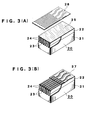
- A first preferred embodiment of the present invention will now be described with reference to Figs. 1 to 4C. The structure of an ink jet printer head according to the first preferred embodiment will first be described with reference to Figs. 2Ato 4C in the order of the manufacturing steps of the inkjet printer head. As shown in Fig. 2A, a
substrate 20 is first manufactured. More specifically, a fluidic resin to be formed into a low-rigid member 22 having a rigidity lower than that of a plate-Ii kepiezoelectric member 21 is applied over the upper surface of thepiezoelectric member 21. Thepiezoelectric member 21 is formed from a lead zirconate titanate piezoelectric ceramic plate polarized across the thickness thereof. The fluidic resin used herein is a two-liquid mixing type of epoxy adhesive containing an inorganic filler in consideration of an adhesive strength, ease of after-treatment, adhesion of plating in forming electrodes, coefficient of linear expansion, etc. The epoxy adhesive is applied to thepiezoelectric member 21 over the upper surface thereof so that no bubbles are left in the coating of the epoxy adhesive. Then, the coating of the epoxy adhesive is cured to thereby form the low-rigid member 22 fixed to the upper surface of thepiezoelectric member 21. - In the next step, the upper surface of the low-
rigid member 22 is ground to a flat surface with reference to the upper surface of thepiezoelectric member 21. Then, as shown in Fig. 2B, thesubstrate 20 is cut from the upper surface of the low-rigid member 22 with a depth beyond the bonded surface between the low-rigid member22 and the piezoelectric member21 to form a plurality ofgrooves 23 spaced a given distance from each other. The formation of theplural grooves 23 results in formation of a plurality ofside walls 24, any adjacent ones of which are formed on the opposed sides of eachgroove 23. Eachside wall 24 includes an upper side wall 24a formed from the low-rigid member 22 and alower side wall 24b formed from thepiezoelectric member 21. This cutting of thesubstrate 20 is performed by using a diamond wheel for use in cutting of an IC wafer. Eachgroove 23 is formed so that one longitudinal end thereof is opened to one longitudinal end surface of thesubstrate 20 and that the other longitudinal end is not opened to the other end surface of thesubstrate 20. Accordingly, a part of the upper surface of thesubstrate 20 on the closed side of thegrooves 23 is left as a flat surface. This flat portion of thesubstrate 20 is formed as a wiringpattern forming surface 61 on which a plurality ofwiring patterns 29 are to be formed as will be hereinafter described. - In the next step, washing, catalyzing, and accelerating are performed as a pretreatment of formation of electrodes by electroless plating. The washing is performed for the purposes of activating a plating forming surface and making the. surface of the
substrate 20 hydrophilic to facilitate entry of a catalyst liquid, accelerator liquid, and plating liquid into thegrooves 23. The catalyzing is next performed for the purpose of adsorbing a complex of Pd and Sn on the inner surface of eachgroove 23 by immersing thesubstrate 20 into the catalyst liquid as a pretreatment liquid containing palladium chloride, stannous chloride, and concentrated sulfuric acid. The catalyzing allows the complex of Pd and Sn to be adsorbed on the surface of the low-rigid member 22 and the inner surface of eachgroove 23 formed by the upper side wall 24a and thelower side wall 24b. The accelerating is next performed for the purpose of making the complex adsorbed in the catalyzing process into a catalyst, so that the complex adsorbed on theside walls 24, etc. is made into metallized Pd as a catalyst core. - In the next step, a mask is formed on the upper surface of the low-
rigid member 22 except a wiring pattern forming portion. More specifically, as shown in Fig. 2C, adry film 25 is attached to the upper surface of the low-rigid member 22. Then, as shown in Fig. 3A, a resistmask 26 is placed on thedry film 25. In this condition, exposure and development are performed to thedry film 25. Accordingly, as shown in Fig. 3B, a resistfilm 27 is formed from thedry film 25 on the upper surface of the low-rigid member 22 except the wiring pattern forming portion. In this condition, the metallized Pd is exposed from the wiring pattern forming portion of the low-rigid member 22 and the inner surface of eachgroove 23. - In the next step, the
substrate 20 is immersed into the plating liquid to perform electroless plating. The plating liquid is composed of a main component containing a metal salt and a reducing agent and an auxiliary component containing a pH adjusting agent, a buffering agent, a complexing agent, an accelerating agent, a stabilizing agent, and a modifying agent. Thesubstrate 20 as a bonded body (a subject body to be plated) formed by bonding thepiezoelectric member 21 and the low-rigid member 22 is immersed into the plating liquid to form a plating with the metallized Pd functioning as a catalyst core. Accordingly, as shown in Fig. 4A, a plurality ofelectrodes 28 are formed on the inner side surfaces of thegrooves 23, i.e., the side surfaces of theside walls 24, and the bottom surfaces of thegrooves 23. Further, a plurality ofwiring patterns 29 contiguous to theelectrodes 28 are also formed on the upper surface of the low-rigid member 22, i.e., on the wiringpattern forming surface 61. - In the next step, the resist
film 27 attached to the upper surface of the low-rigid member 22 is separated off as shown in Fig. 4B. Then, as shown in Fig. 4C, atop plate 30 is bonded to the upper surface of the low-rigid member 22. In this condition, all thegrooves 23 are closed at their upper openings to define a plurality of pressure chambers 34 (see Fig. 1). In bonding thetop plate 30 to the upper surface of the low-rigid member 22, there occurs a step at the boundary between the front end surface of thesubstrate 20 and the front end surface of thetop plate 30. Accordingly, this step is removed by grinding both the front end surfaces of thesubstrate 20 and thetop plate 30. Thereafter, anozzle plate 32 having a plurality ofink jet nozzles 31 respectively communicating with the front end openings of thegrooves 23 is fixed to both the flushed front end surfaces of thesubstrate 20 and thetop plate 30. Then, anink supply pipe 33 as an ink supply member for supplying ink from an ink supply passage (not shown) to eachgroove 23 is mounted to thetop plate 30, thereby completing the inkjet printer head. - Fig. 1 shows a front elevational view of the inkjet printer head thus manufactured in the condition where the
nozzle plate 32 is removed. In Fig. 1, arrows show a direction of polarization of thepiezoelectric member 21. Electric fields are applied both to theelectrodes 28 in thepressure chamber 34 from which the ink is intended to be jetted and to theelectrodes 28 in the twopressure chambers 34 formed adjacent to the intendedpressure chamber 34. Accordingly, the twoside walls 24 adjacent to the intendedpressure chamber 34 are symmetrically displaced to thereby suck or jet the ink. - In Fig. 1, phantom lines shown in the
central pressure chamber 34 indicate a condition that the twoside walls 24 adjacent to thecentral pressure chamber 34 are inwardly deformed, so as to increase the pressure in thecentral pressure chamber 34 and thereby jet the ink therefrom. As an upper part of eachside wall 34 is formed as the upper side wall 24a formed from the low-rigid member 22, the resistance of the upper side wall 24a against the operation of thelower side wall 24b formed from thepiezoelectric member 21 can be reduced to thereby allow large operation of eachside wall 24 as a whole. Furthermore, as thewiring patterns 29 of the ink jet printer head manufactured above are provided on the low-rigid member 22 having a low permittivity (having a specific permittivity of 3.8 to 4.7 in this preferred embodiment), the electrostatic capacity between thewiring patterns 29 can be greatly reduced as compared with the conventional structure that the wiring patterns are provided on the piezoelectric member (having a specific permittivity of 1500 to 4700). Accordingly, in applying voltage across theelectrodes 28 in thepressure chamber 34, electric current flowing through theelectrodes 28 can be reduced, and the time period from the instance of application of voltage to theelectrodes 28 to the instance the voltage applied to theelectrodes 28 reaches a given voltage can be shortened. Owing to these advantages, the inkjet characteristics of the inkjet printer head can be improved. - Although the low-
rigid member 22 is formed of adhesive in this preferred embodiment, the material of the low-rigid member 22 is not limited to adhesive. For example, a molded plate formed of a resin material may be used for the low-rigid member 22. Also in this case, the objects of the present invention can be attained. Further, although theelectrodes 28 and thewiring patterns 29 are formed by electroless plating in this preferred embodiment, the forming method for theelectrodes 28 and thewiring patterns 29 is not limited to electroless plating. For example, theelectrodes 28 and thewiring patterns 29 may be formed by vapor deposition. - A second preferred embodiment of the present invention is shown in Fig. 5. The same parts as those in the first preferred embodiment are denoted by the same reference numerals. In this preferred embodiment,
reference numeral 36 denotes a substrate composed of abottom plate 35 formed of a material having a high rigidity and a low thermal deformability, such as ceramics or glass, apiezoelectric member 21 fixed to the upper surface of thebottom plate 35, and a low-rigid member 22 fixed to the upper surface of thepiezoelectric member 21. This structure is intended to increase the strength of the ink jet printer head. The other construction includingpressure chambers 34,electrodes 28, andwiring patterns 29 is similar to that in the first preferred embodiment, and the description thereof will be omitted herein. - In the second preferred embodiment,
grooves 23 defining thepressure chambers 34 are formed with a depth reaching the upper surface of thebottom plate 35. Accordingly, thegrooves 23 can be easily formed to have a uniform depth. Alternatively, the depth of eachgroove 23 may be set so as not to reach the upper surface of thebottom plate 35. Also with this structure, the effect of increasing the strength of the ink jet printer head can be retained. - Having thus described specific preferred embodiments of the present invention, it is to be noted that these preferred embodiments are merely illustrative and are intended not to limit the present invention. The scope of the present invention is not to be construed as identical with that of the above preferred embodiments. Actually, various modifications may be made within the scope of the present invention as defined in the appended claims.
Claims (16)
Applications Claiming Priority (3)
| Application Number | Priority Date | Filing Date | Title |
|---|---|---|---|
| JP6069186A JPH07276624A (en) | 1994-04-07 | 1994-04-07 | Ink jet printer head |
| JP6918694 | 1994-04-07 | ||
| JP69186/94 | 1994-04-07 |
Publications (3)
| Publication Number | Publication Date |
|---|---|
| EP0676286A2 true EP0676286A2 (en) | 1995-10-11 |
| EP0676286A3 EP0676286A3 (en) | 1997-01-22 |
| EP0676286B1 EP0676286B1 (en) | 1999-12-29 |
Family
ID=13395451
Family Applications (1)
| Application Number | Title | Priority Date | Filing Date |
|---|---|---|---|
| EP95302236A Expired - Lifetime EP0676286B1 (en) | 1994-04-07 | 1995-04-04 | Ink jet printer head |
Country Status (5)
| Country | Link |
|---|---|
| US (1) | US5696545A (en) |
| EP (1) | EP0676286B1 (en) |
| JP (1) | JPH07276624A (en) |
| KR (1) | KR0175971B1 (en) |
| DE (1) | DE69514134T2 (en) |
Cited By (3)
| Publication number | Priority date | Publication date | Assignee | Title |
|---|---|---|---|---|
| EP0870616A2 (en) * | 1997-04-09 | 1998-10-14 | Brother Kogyo Kabushiki Kaisha | A method for producing an ink jet head |
| WO2001012442A3 (en) * | 1999-08-14 | 2001-07-05 | Xaar Technology Ltd | Droplet deposition apparatus |
| EP2078611A1 (en) * | 2008-01-11 | 2009-07-15 | SII Printek Inc | Inkjet head chip, manufacturing method for inkjet head chip, inkjet head, and inkjet recording apparatus |
Families Citing this family (7)
| Publication number | Priority date | Publication date | Assignee | Title |
|---|---|---|---|---|
| JP3637633B2 (en) * | 1995-05-10 | 2005-04-13 | ブラザー工業株式会社 | Ink jet print head and method for manufacturing the same |
| US5793149A (en) * | 1995-07-26 | 1998-08-11 | Francotyp-Postalia Ag & Co. | Arrangement for plate-shaped piezoactuators and method for the manufacture thereof |
| JPH1191102A (en) * | 1997-09-25 | 1999-04-06 | Nec Corp | Solid actuator and ink-jet head |
| US6402818B1 (en) * | 2000-06-02 | 2002-06-11 | Celgard Inc. | Degassing a liquid with a membrane contactor |
| JP5689651B2 (en) * | 2010-11-09 | 2015-03-25 | エスアイアイ・プリンテック株式会社 | Liquid ejecting head, liquid ejecting apparatus, and liquid ejecting head driving method |
| JP5626250B2 (en) * | 2012-03-30 | 2014-11-19 | ブラザー工業株式会社 | Droplet ejector and piezoelectric actuator |
| WO2020159517A1 (en) | 2019-01-31 | 2020-08-06 | Hewlett-Packard Development Company, L.P. | Fluidic die with surface condition monitoring |
Citations (4)
| Publication number | Priority date | Publication date | Assignee | Title |
|---|---|---|---|---|
| WO1992009436A1 (en) * | 1990-11-27 | 1992-06-11 | Xaar Limited | Laminate for use in manufacture of ink jet printheads |
| EP0533506A2 (en) * | 1991-09-19 | 1993-03-24 | Brother Kogyo Kabushiki Kaisha | Ink droplet ejection device |
| EP0565280A2 (en) * | 1992-03-26 | 1993-10-13 | Kabushiki Kaisha TEC | Method of producing printer head using piezoelectric member |
| EP0639460A1 (en) * | 1993-08-20 | 1995-02-22 | Kabushiki Kaisha TEC | Method of fabricating ink jet print head |
Family Cites Families (8)
| Publication number | Priority date | Publication date | Assignee | Title |
|---|---|---|---|---|
| US4879568A (en) * | 1987-01-10 | 1989-11-07 | Am International, Inc. | Droplet deposition apparatus |
| GB8824014D0 (en) * | 1988-10-13 | 1988-11-23 | Am Int | High density multi-channel array electrically pulsed droplet deposition apparatus |
| JP2744536B2 (en) * | 1991-10-04 | 1998-04-28 | 株式会社テック | Ink jet printer head and method of manufacturing the same |
| JPH04363250A (en) * | 1991-03-19 | 1992-12-16 | Tokyo Electric Co Ltd | Ink jet printer head and method for its production |
| JPH04357037A (en) * | 1991-03-19 | 1992-12-10 | Tokyo Electric Co Ltd | Ink jet printer head |
| JP2744535B2 (en) * | 1991-07-08 | 1998-04-28 | 株式会社テック | Method of manufacturing ink jet printer head |
| JP2843199B2 (en) * | 1992-03-26 | 1999-01-06 | 株式会社テック | Method of manufacturing ink jet printer head |
| US5459501A (en) * | 1993-02-01 | 1995-10-17 | At&T Global Information Solutions Company | Solid-state ink-jet print head |
-
1994
- 1994-04-07 JP JP6069186A patent/JPH07276624A/en active Pending
-
1995
- 1995-03-30 KR KR1019950007034A patent/KR0175971B1/en not_active IP Right Cessation
- 1995-04-04 EP EP95302236A patent/EP0676286B1/en not_active Expired - Lifetime
- 1995-04-04 DE DE69514134T patent/DE69514134T2/en not_active Expired - Fee Related
- 1995-04-06 US US08/417,786 patent/US5696545A/en not_active Expired - Lifetime
Patent Citations (4)
| Publication number | Priority date | Publication date | Assignee | Title |
|---|---|---|---|---|
| WO1992009436A1 (en) * | 1990-11-27 | 1992-06-11 | Xaar Limited | Laminate for use in manufacture of ink jet printheads |
| EP0533506A2 (en) * | 1991-09-19 | 1993-03-24 | Brother Kogyo Kabushiki Kaisha | Ink droplet ejection device |
| EP0565280A2 (en) * | 1992-03-26 | 1993-10-13 | Kabushiki Kaisha TEC | Method of producing printer head using piezoelectric member |
| EP0639460A1 (en) * | 1993-08-20 | 1995-02-22 | Kabushiki Kaisha TEC | Method of fabricating ink jet print head |
Cited By (7)
| Publication number | Priority date | Publication date | Assignee | Title |
|---|---|---|---|---|
| EP0870616A2 (en) * | 1997-04-09 | 1998-10-14 | Brother Kogyo Kabushiki Kaisha | A method for producing an ink jet head |
| EP0870616A3 (en) * | 1997-04-09 | 1999-03-31 | Brother Kogyo Kabushiki Kaisha | A method for producing an ink jet head |
| US6070310A (en) * | 1997-04-09 | 2000-06-06 | Brother Kogyo Kabushiki Kaisha | Method for producing an ink jet head |
| WO2001012442A3 (en) * | 1999-08-14 | 2001-07-05 | Xaar Technology Ltd | Droplet deposition apparatus |
| US6725543B2 (en) | 1999-08-14 | 2004-04-27 | Xaar Technology Limited | Droplet deposition apparatus |
| EP2078611A1 (en) * | 2008-01-11 | 2009-07-15 | SII Printek Inc | Inkjet head chip, manufacturing method for inkjet head chip, inkjet head, and inkjet recording apparatus |
| US7950781B2 (en) | 2008-01-11 | 2011-05-31 | Sii Printek Inc. | Inkjet head chip, manufacturing method for inkjet head chip, inkjet head, and inkjet recording apparatus |
Also Published As
| Publication number | Publication date |
|---|---|
| KR950028921A (en) | 1995-11-22 |
| EP0676286B1 (en) | 1999-12-29 |
| JPH07276624A (en) | 1995-10-24 |
| US5696545A (en) | 1997-12-09 |
| DE69514134T2 (en) | 2000-05-25 |
| KR0175971B1 (en) | 1999-05-15 |
| DE69514134D1 (en) | 2000-02-03 |
| EP0676286A3 (en) | 1997-01-22 |
Similar Documents
| Publication | Publication Date | Title |
|---|---|---|
| US5471232A (en) | Ink jet recording head | |
| US5684519A (en) | Ink jet head with buckling structure body | |
| KR960003339B1 (en) | Ink-jet head and the method of fabricating the same | |
| KR960012756B1 (en) | Method of producing printer-head using piezoelectric member | |
| AU684797B2 (en) | Single side drive system interconnectable ink jet printhead and method of manufacturing the same | |
| US5696545A (en) | Ink jet printer head | |
| US5301404A (en) | Method of producing printer head using piezoelectric member | |
| JPH04357037A (en) | Ink jet printer head | |
| EP0639460B1 (en) | Method of fabricating ink jet print head | |
| EP0795404B1 (en) | Ink jet recording head | |
| KR20040072471A (en) | Method for producing ink jet head | |
| US5594475A (en) | Ink jet printer head and a method of driving the same | |
| EP0867287B1 (en) | Ink jet recording head | |
| JPH09300609A (en) | Ink-jet head | |
| US6431690B1 (en) | Ink jet head and producing process therefor | |
| US7163279B2 (en) | Inkjet head having relay member interposed between piezoelectric element and diaphragm | |
| JP2861117B2 (en) | Ink jet printer head and method of manufacturing the same | |
| JPH10157144A (en) | Production of ink jet printing head | |
| JP2000218792A (en) | Ink jet head | |
| JPS61125859A (en) | Ink jet recording head | |
| JP3744687B2 (en) | Inkjet recording head and inkjet recording apparatus | |
| JPH07156399A (en) | Ink jet recording head, and its production method | |
| KR100245474B1 (en) | Piezoelectric film forming method of print head | |
| JPH0747678A (en) | Manufacture of ink jet printer head | |
| JPH10235862A (en) | Connection structure of lead terminal |
Legal Events
| Date | Code | Title | Description |
|---|---|---|---|
| PUAI | Public reference made under article 153(3) epc to a published international application that has entered the european phase |
Free format text: ORIGINAL CODE: 0009012 |
|
| 17P | Request for examination filed |
Effective date: 19950411 |
|
| AK | Designated contracting states |
Kind code of ref document: A2 Designated state(s): DE GB SE |
|
| PUAL | Search report despatched |
Free format text: ORIGINAL CODE: 0009013 |
|
| AK | Designated contracting states |
Kind code of ref document: A3 Designated state(s): DE GB SE |
|
| 17Q | First examination report despatched |
Effective date: 19971209 |
|
| GRAG | Despatch of communication of intention to grant |
Free format text: ORIGINAL CODE: EPIDOS AGRA |
|
| GRAG | Despatch of communication of intention to grant |
Free format text: ORIGINAL CODE: EPIDOS AGRA |
|
| GRAH | Despatch of communication of intention to grant a patent |
Free format text: ORIGINAL CODE: EPIDOS IGRA |
|
| RAP1 | Party data changed (applicant data changed or rights of an application transferred) |
Owner name: TOSHIBA TEC KABUSHIKI KAISHA |
|
| GRAH | Despatch of communication of intention to grant a patent |
Free format text: ORIGINAL CODE: EPIDOS IGRA |
|
| GRAA | (expected) grant |
Free format text: ORIGINAL CODE: 0009210 |
|
| AK | Designated contracting states |
Kind code of ref document: B1 Designated state(s): DE GB SE |
|
| REF | Corresponds to: |
Ref document number: 69514134 Country of ref document: DE Date of ref document: 20000203 |
|
| PLBE | No opposition filed within time limit |
Free format text: ORIGINAL CODE: 0009261 |
|
| STAA | Information on the status of an ep patent application or granted ep patent |
Free format text: STATUS: NO OPPOSITION FILED WITHIN TIME LIMIT |
|
| 26N | No opposition filed | ||
| REG | Reference to a national code |
Ref country code: GB Ref legal event code: IF02 |
|
| PGFP | Annual fee paid to national office [announced via postgrant information from national office to epo] |
Ref country code: SE Payment date: 20060406 Year of fee payment: 12 |
|
| PG25 | Lapsed in a contracting state [announced via postgrant information from national office to epo] |
Ref country code: SE Free format text: LAPSE BECAUSE OF NON-PAYMENT OF DUE FEES Effective date: 20070405 |
|
| PGFP | Annual fee paid to national office [announced via postgrant information from national office to epo] |
Ref country code: DE Payment date: 20090402 Year of fee payment: 15 |
|
| PGFP | Annual fee paid to national office [announced via postgrant information from national office to epo] |
Ref country code: GB Payment date: 20090401 Year of fee payment: 15 |
|
| GBPC | Gb: european patent ceased through non-payment of renewal fee |
Effective date: 20100404 |
|
| PG25 | Lapsed in a contracting state [announced via postgrant information from national office to epo] |
Ref country code: DE Free format text: LAPSE BECAUSE OF NON-PAYMENT OF DUE FEES Effective date: 20101103 |
|
| PG25 | Lapsed in a contracting state [announced via postgrant information from national office to epo] |
Ref country code: GB Free format text: LAPSE BECAUSE OF NON-PAYMENT OF DUE FEES Effective date: 20100404 |