EP0675606A1 - Receiver for spread spectrum communication - Google Patents
Receiver for spread spectrum communication Download PDFInfo
- Publication number
- EP0675606A1 EP0675606A1 EP94929641A EP94929641A EP0675606A1 EP 0675606 A1 EP0675606 A1 EP 0675606A1 EP 94929641 A EP94929641 A EP 94929641A EP 94929641 A EP94929641 A EP 94929641A EP 0675606 A1 EP0675606 A1 EP 0675606A1
- Authority
- EP
- European Patent Office
- Prior art keywords
- signal
- circuit
- signals
- frequency
- correcting
- Prior art date
- Legal status (The legal status is an assumption and is not a legal conclusion. Google has not performed a legal analysis and makes no representation as to the accuracy of the status listed.)
- Granted
Links
Images


Classifications
-
- H—ELECTRICITY
- H04—ELECTRIC COMMUNICATION TECHNIQUE
- H04B—TRANSMISSION
- H04B1/00—Details of transmission systems, not covered by a single one of groups H04B3/00 - H04B13/00; Details of transmission systems not characterised by the medium used for transmission
- H04B1/69—Spread spectrum techniques
- H04B1/707—Spread spectrum techniques using direct sequence modulation
- H04B1/7097—Interference-related aspects
- H04B1/711—Interference-related aspects the interference being multi-path interference
- H04B1/7115—Constructive combining of multi-path signals, i.e. RAKE receivers
- H04B1/7117—Selection, re-selection, allocation or re-allocation of paths to fingers, e.g. timing offset control of allocated fingers
Definitions
- the present invention relates to a receiver of a code division multiple access (CDMA) communication system appropriate for mobile communica tions, and particularly to a spread spectrum communication receiver which corrects a frequency offset of a local signal with respect to a received signal in a baseband signal region.
- CDMA code division multiple access
- baseband signal in this specification refers to a signal having no carrier signal components. More specifically, the baseband signal at a transmitter refers to a signal after the primary modulation or a signal after spreading, and the baseband signal at a receiver refers to a signal after quadrature detection and before despreading, and a signal after despreading.
- the CDMA system falls into a direct sequence (DC) system and a frequency hopping (FH) system.
- the FH system is seldom used at present. This is because the FH system resolves a symbol into elements called chips, and translates individual chips into carriers of different frequencies at a high rate, which is difficult to be implemented by a frequency synthesizer in the state of the art.
- the DS system performs, at a transmitter, a primary modulation of an original signal use in QPSK or the like, spreading (secondary modulation) of the primary modulated signal into a wideband signal using a spreading code, and transmission thereof on a carrier, and at a receiver, removal of the carrier, despreading (secondary demodulation) of the wideband signal into the primary modulated signal using the spreading code identical to that of the transmitter, and recovery of the original signal by a primary demodulation.
- Base station equipment of mobile communications today includes a highly stable reference oscillator, and the accuracy under the domestic standard for digital vehicle telephony in Japan is less than 0.05 ppm in absolute accuracy.
- mobile station equipment usually employs a temperature compensated crystal oscillator (TCXO) because of difficulty of using a highly stable reference oscillator with a thermostat.
- TCXO temperature compensated crystal oscillator
- the frequency accuracy of the crystal oscillators is approximately 3 ppm in absolute accuracy in an 800 MHz band.
- the frequency of the local signal of a mobile station will deviate from the center frequency of a transmitted signal of a base station (that is, a received signal of the mobile station).
- an AFC Automatic Frequency Control
- the center frequency of the received signal further deviates by an amount corresponding to the Doppler frequency.
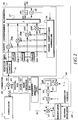
- Fig. 1 shows a major portion of a conventional CDMA receiver with an AFC circuit.
- An intermediate frequency (IF) received signal applied to an input terminal 10 is divided into two parts by a hybrid coil 10A, and is supplied to a quadrature detector 11.
- the quadrature detector 11 detects the IF received signal by a local signal from a voltage controlled oscillator (VCO) 12, and outputs an in-phase baseband signal I and a quadrature baseband signal Q.
- VCO voltage controlled oscillator
- I baseband signal is supplied to an A/D converter 15 through an LPF (lowpass filter) 13, and is converted into a digital signal.
- the Q baseband signal is supplied to an A/D converter 16 through an LPF 14, and is converted into a digital signal.
- a correlator 17 consisting of matched filters or a sliding correlator, which detects correlation between the received digital signals and the spreading code, thereby despreading the digital signals.
- the correlator 17 functions as a despreader, and outputs baseband signals corresponding to the primary modulated signal.
- the outputs of the correlator 17 are supplied to a RAKE receiver and demodulator 18 which demodulates the baseband signals corresponding to the primary modulated signal and recovers the original signal.
- An AFC circuit 20 is arranged as follows: The outputs of the correlator 17 are supplied to a differential demodulator 21. Signals undergone the differential demodulation are supplied to a phase error detector 22.
- the phase error detector 22 obtains a phase error component tan ⁇ 1(Q/I) from the amplitudes of the I and Q signals, and outputs it.
- This output signal represents a phase rotation component, that is, a phase error at the receiver with respect to a mapped point of the primary modulated signal at the transmitter.
- a phase error signal is obtained which is proportional to a frequency error between the received signal and the local signal.
- the phase error signal is averaged by a loop filter 23, and fed back to the VCO 12 as a control voltage.
- the VCO 12 undergoes feedback control by the error correcting voltage corresponding to the phase error signal, so that the frequency error between the center frequency of the received signal and the frequency of the local signal is corrected.
- an object of the present invention is to provide a spread spectrum communication receiver which is appropriate to be embedded into an IC, and is inexpensive.
- a spread spectrum communication receiver comprising: a detector for detecting a received signal using a local signal, thereby converting the received signal into a first baseband signal; a despreader for despreading the first baseband signal using a spreading code, thereby outputting a second baseband signal corresponding to a primary modulated signal at a transmitter; a corrector for correcting the second baseband signal by a correcting signal; an interference eliminator for suppressing an interference component in a third baseband signal outputted from the corrector, thereby generating a desired signal component; a remodulator for modulating the desired signal component, thereby generating a remodulated signal corresponding to the primary modulated signal at the transmitter; a multiplier for multiplying the second baseband signal by a complex conjugate signal of the remodulated signal, thereby outputting a signal including a frequency offset component representing an offset frequency corresponding to a deviation of the frequency of the local signal with respect to the center frequency of the received signal
- the correcting signal generator may comprise a fast Fourier transform circuit for Fourier transforming the frequency offset component, a peak detector for detecting a peak of an output of the fast Fourier transform circuit, and a digital voltage controlled oscillator for generating the correcting signal by oscillating at a frequency corresponding to the peak.
- the interference eliminator may comprise an adaptive RAKE circuit.
- the spread spectrum communication receiver may further comprise: a memory circuit for storing a pattern of a known unique word; a detector for detecting a start of receiving the unique word from the second baseband signal; and a selector for selectively providing the remodulator with the unique word from the memory circuit when the detector detects the start of receiving the unique word, and with an output of the interference eliminator when the detector detects an end of receiving the unique word.
- an offset between the center frequency of the received signal and the frequency of the local signal is corrected by a digital signal processing in a baseband signal domain.
- a highly accurate, highly stable oscillator which is required in the conventional local signal oscillator to convert the received signal into the baseband signal, can be obviated. This makes it possible to reduce the cost of the mobile unit.
- a double slash mark (//) on lines indicates that the lines are a double line. Accordingly, signals on these lines can be handled as a complex number.
- Fig. 2 is a block diagram showing a first embodiment of a spread spectrum communication receiver in accordance with the present invention.
- the signal S1 is multiplied at a corrector 25 by a correcting signal S2 which will be described later, thereby being corrected.
- the corrected signal S3 is supplied to an adaptive RAKE circuit 30 functioning as an interference eliminator.
- the adaptive RAKE circuit 30 includes a sampling circuit 31 that samples that signal S3; delay circuits 32B - 32D that delay the output of the sampling circuit 31 by predetermined time periods; multipliers 35A - 35D that multiply the output of the sampler 31 and the outputs of the delay circuits 32B - 32D by tapped coefficients a1 - a4, respectively; a tapped coefficient controller 36 that generates the tapped coefficients a1 - a4 on the basis of the output of the sampling circuit 31, the outputs of the delay circuits 32B - 32D, and the output of an adder 39 which will be described below; an integrator 37 that sums the outputs of the multipliers 35A - 35D; a decision circuit 38 that decides a summed output S4, and produces the decided output (desired wave component) S5; and the adder 39 that outputs the difference between the output S5 of the decision circuit 38 and the output S4 of the integrator 37.
- the decided output (desired wave component ) S5 is supplied to a reverse modulator 40 including a remodulator 41 and a multiplier 42.
- the remodulator 41 remoudlates the decided output S5 in a manner similar to the primary modulation at the transmitter, thereby outputting a remodulated signal S6.
- the remodulated signal S6 can be expressed as
- the multiplier 42 multiplies the complex conjugate of the remodulated signal S6 by the input baseband signal S1, thereby outputting a signal S7.
- the signal S7 can be expressed as follows: where ⁇ ( t ) ⁇ ⁇ ⁇ ( t ) .
- the signal S7 outputted from the reverse modulator 40 is averaged by an averaging circuit 50 which eliminates the thermal noise component N ( t ) ⁇ e - j ⁇ ( t ) , thereby producing only the frequency offset component R ⁇ e j ⁇ ⁇ t .
- the averaging circuit 50 includes a multiplier 51, an adder 52, a delay circuit 53, and a multiplier 54.
- the multiplier 51 multiplies the signal S7 by a predetermined fixed value ⁇ .
- the adder 52 adds the outputs of the multipliers 51 and 54.
- the delay circuit 53 delays the output of the adder 52 by a time period T.
- the multiplier 54 multiplies the output of the delay circuit 53 by a fixed value (1- ⁇ ).
- the averaging circuit 50 averages the signal S7, and outputs a signal S8 that includes only the frequency offset component of the signal S7.
- the signal 58 is supplied to a frequency analyzer 61.
- the frequency analyzer 61 is an FFT circuit that Fourier transforms the frequency offset component R ⁇ e j ⁇ ⁇ t .
- the frequency analyzer 61 outputs a signal S9, in which a line spectrum stands at an angular frequency ⁇ .
- the signal S9 is fed to a peak detector 62.
- the peak detector 62 obtains an angular frequency ⁇ corresponding to the peak, and supplied a frequency control signal S10 corresponding to the angular frequency to a digital VCO 63.
- the digital VCO 63 outputs the correcting signal S2 with the angular frequency ⁇ and a phase opposite to that of the signal S1.
- the correcting signal S2 is supplied to the corrector 25, which multiplies the input baseband signal S1 by the correcting signal S2, thereby eliminating the frequency offset component of the signal S1.
- Fig. 3 is a block diagram showing the major portion of a second embodiment of a spread spectrum communication receiver in accordance with the present invention.
- the second embodiment differs from the first embodiment in the following:
- the selector 82 provides the remodulator 41 with the unique word S12 read from the unique word memory circuit 81 while receiving a unique word, and with the output S5 of the decision circuit 38 while receiving information.
- a correct remodulated signal S6 can always be obtained while receiving a known unique word.
- the second embodiment can eliminate the frequency offset component at higher accuracy than the first embodiment.
Abstract
Description
- The present invention relates to a receiver of a code division multiple access (CDMA) communication system appropriate for mobile communica tions, and particularly to a spread spectrum communication receiver which corrects a frequency offset of a local signal with respect to a received signal in a baseband signal region.
- The term "baseband signal" in this specification refers to a signal having no carrier signal components. More specifically, the baseband signal at a transmitter refers to a signal after the primary modulation or a signal after spreading, and the baseband signal at a receiver refers to a signal after quadrature detection and before despreading, and a signal after despreading.
- Recently, tremendous research and development effort has been directed to CDMA systems. The CDMA system falls into a direct sequence (DC) system and a frequency hopping (FH) system. The FH system is seldom used at present. This is because the FH system resolves a symbol into elements called chips, and translates individual chips into carriers of different frequencies at a high rate, which is difficult to be implemented by a frequency synthesizer in the state of the art.
- Thus, the DS system is commonly used. The DS system performs, at a transmitter, a primary modulation of an original signal use in QPSK or the like, spreading (secondary modulation) of the primary modulated signal into a wideband signal using a spreading code, and transmission thereof on a carrier, and at a receiver, removal of the carrier, despreading (secondary demodulation) of the wideband signal into the primary modulated signal using the spreading code identical to that of the transmitter, and recovery of the original signal by a primary demodulation.
- Problems involved in applying the CDMA system to mobile communication systems such as portable telephony will be considered. Base station equipment of mobile communications today includes a highly stable reference oscillator, and the accuracy under the domestic standard for digital vehicle telephony in Japan is less than 0.05 ppm in absolute accuracy. On the other hand, mobile station equipment usually employs a temperature compensated crystal oscillator (TCXO) because of difficulty of using a highly stable reference oscillator with a thermostat. The frequency accuracy of the crystal oscillators is approximately 3 ppm in absolute accuracy in an 800 MHz band.
- As a result, the frequency of the local signal of a mobile station will deviate from the center frequency of a transmitted signal of a base station (that is, a received signal of the mobile station). To compensate for the offset of the frequency to maintain stable receiving operation, an AFC (Automatic Frequency Control) circuit is required. In addition, since a mobile station is usually moving with respect to the base station, the center frequency of the received signal further deviates by an amount corresponding to the Doppler frequency.
- Fig. 1 shows a major portion of a conventional CDMA receiver with an AFC circuit. An intermediate frequency (IF) received signal applied to an
input terminal 10 is divided into two parts by ahybrid coil 10A, and is supplied to aquadrature detector 11. Thequadrature detector 11 detects the IF received signal by a local signal from a voltage controlled oscillator (VCO) 12, and outputs an in-phase baseband signal I and a quadrature baseband signal Q. These baseband signals are baseband signals spread by a spreading code. The I baseband signal is supplied to an A/D converter 15 through an LPF (lowpass filter) 13, and is converted into a digital signal. Likewise, the Q baseband signal is supplied to an A/D converter 16 through anLPF 14, and is converted into a digital signal. - These digital signals are fed to a
correlator 17 consisting of matched filters or a sliding correlator, which detects correlation between the received digital signals and the spreading code, thereby despreading the digital signals. In other words, thecorrelator 17 functions as a despreader, and outputs baseband signals corresponding to the primary modulated signal. The outputs of thecorrelator 17 are supplied to a RAKE receiver anddemodulator 18 which demodulates the baseband signals corresponding to the primary modulated signal and recovers the original signal. - An
AFC circuit 20 is arranged as follows: The outputs of thecorrelator 17 are supplied to adifferential demodulator 21. Signals undergone the differential demodulation are supplied to a phase error detector 22. The phase error detector 22 obtains a phase error component
loop filter 23, and fed back to theVCO 12 as a control voltage. Thus, theVCO 12 undergoes feedback control by the error correcting voltage corresponding to the phase error signal, so that the frequency error between the center frequency of the received signal and the frequency of the local signal is corrected. - According to this method, a problem arises in that the mobile unit becomes expensive because a highly accurate, highly stable VCO is required as the
VCO 12. - Therefore, an object of the present invention is to provide a spread spectrum communication receiver which is appropriate to be embedded into an IC, and is inexpensive.
- In a first aspect of the present invention, there is provided a spread spectrum communication receiver comprising:
a detector for detecting a received signal using a local signal, thereby converting the received signal into a first baseband signal;
a despreader for despreading the first baseband signal using a spreading code, thereby outputting a second baseband signal corresponding to a primary modulated signal at a transmitter;
a corrector for correcting the second baseband signal by a correcting signal;
an interference eliminator for suppressing an interference component in a third baseband signal outputted from the corrector, thereby generating a desired signal component;
a remodulator for modulating the desired signal component, thereby generating a remodulated signal corresponding to the primary modulated signal at the transmitter;
a multiplier for multiplying the second baseband signal by a complex conjugate signal of the remodulated signal, thereby outputting a signal including a frequency offset component representing an offset frequency corresponding to a deviation of the frequency of the local signal with respect to the center frequency of the received signal;
an averaging circuit for averaging an output of the multiplier to eliminated noise components of the output of the multiplier, thereby outputting the frequency offset component; and
a correcting signal generator for generating the correcting signal by extracting the offset frequency from the frequency offset component. - The correcting signal generator may comprise a fast Fourier transform circuit for Fourier transforming the frequency offset component, a peak detector for detecting a peak of an output of the fast Fourier transform circuit, and a digital voltage controlled oscillator for generating the correcting signal by oscillating at a frequency corresponding to the peak.
- The interference eliminator may comprise an adaptive RAKE circuit.
- The spread spectrum communication receiver may further comprise:
a memory circuit for storing a pattern of a known unique word;
a detector for detecting a start of receiving the unique word from the second baseband signal; and
a selector for selectively providing the remodulator with the unique word from the memory circuit when the detector detects the start of receiving the unique word, and with an output of the interference eliminator when the detector detects an end of receiving the unique word. - According to the present invention, an offset between the center frequency of the received signal and the frequency of the local signal is corrected by a digital signal processing in a baseband signal domain. As a result, a highly accurate, highly stable oscillator, which is required in the conventional local signal oscillator to convert the received signal into the baseband signal, can be obviated. This makes it possible to reduce the cost of the mobile unit.
-
- Fig. 1 is a block diagram showing a major portion of a conventional spread spectrum communication receiver;
- Fig. 2 is a block diagram showing a first embodiment of a spread spectrum communication receiver in accordance with the present invention; and
- Fig. 3 is a block diagram showing a second embodiment of a spread spectrum communication receiver in accordance with the present invention.
- Embodiments of the present invention will now be described with reference to the accompanying drawings. In Figs. 2 and 3, a double slash mark (//) on lines indicates that the lines are a double line. Accordingly, signals on these lines can be handled as a complex number.
- Fig. 2 is a block diagram showing a first embodiment of a spread spectrum communication receiver in accordance with the present invention.
- In Fig. 2, a baseband signal outputted from a correlator (despreader) 17, that is, the despread signal S1, which corresponds to the primary modulated signal, can be expressed as

corrector 25 by a correcting signal S2 which will be described later, thereby being corrected. The corrected signal S3 is supplied to anadaptive RAKE circuit 30 functioning as an interference eliminator. - The
adaptive RAKE circuit 30 includes asampling circuit 31 that samples that signal S3; delaycircuits 32B - 32D that delay the output of thesampling circuit 31 by predetermined time periods;multipliers 35A - 35D that multiply the output of thesampler 31 and the outputs of thedelay circuits 32B - 32D by tapped coefficients a1 - a4, respectively; a tappedcoefficient controller 36 that generates the tapped coefficients a1 - a4 on the basis of the output of thesampling circuit 31, the outputs of thedelay circuits 32B - 32D, and the output of anadder 39 which will be described below; anintegrator 37 that sums the outputs of themultipliers 35A - 35D; adecision circuit 38 that decides a summed output S4, and produces the decided output (desired wave component) S5; and theadder 39 that outputs the difference between the output S5 of thedecision circuit 38 and the output S4 of theintegrator 37. - The decided output (desired wave component ) S5 is supplied to a
reverse modulator 40 including aremodulator 41 and amultiplier 42. Theremodulator 41 remoudlates the decided output S5 in a manner similar to the primary modulation at the transmitter, thereby outputting a remodulated signal S6. The remodulated signal S6 can be expressed as
Themultiplier 42 multiplies the complex conjugate
of the remodulated signal S6 by the input baseband signal S1, thereby outputting a signal S7. The signal S7 can be expressed as follows:
where

reverse modulator 40 separates the baseband signal S1 into the frequency offset component and the thermal noise component. - The signal S7 outputted from the
reverse modulator 40 is averaged by an averagingcircuit 50 which eliminates the thermal noise component

circuit 50 includes amultiplier 51, anadder 52, adelay circuit 53, and amultiplier 54. Themultiplier 51 multiplies the signal S7 by a predetermined fixed value α. Theadder 52 adds the outputs of themultipliers delay circuit 53 delays the output of theadder 52 by a time period T. Themultiplier 54 multiplies the output of thedelay circuit 53 by a fixed value (1-α). Thus, the averagingcircuit 50 averages the signal S7, and outputs a signal S8 that includes only the frequency offset component of the signal S7. - The signal 58 is supplied to a
frequency analyzer 61. Thefrequency analyzer 61 is an FFT circuit that Fourier transforms the frequency offset component R · e j Δωt . Thus, thefrequency analyzer 61 outputs a signal S9, in which a line spectrum stands at an angular frequency Δω. The signal S9 is fed to apeak detector 62. Thepeak detector 62 obtains an angular frequency Δω corresponding to the peak, and supplied a frequency control signal S10 corresponding to the angular frequency to adigital VCO 63. Thus, thedigital VCO 63 outputs the correcting signal S2 with the angular frequency Δω and a phase opposite to that of the signal S1. The correcting signal S2 is supplied to thecorrector 25, which multiplies the input baseband signal S1 by the correcting signal S2, thereby eliminating the frequency offset component of the signal S1. - Fig. 3 is a block diagram showing the major portion of a second embodiment of a spread spectrum communication receiver in accordance with the present invention. The second embodiment differs from the first embodiment in the following:
- (1) A unique word detector 70 for carrying out a frame synchronization is connected to the output of the
correlation detector 17. The unique word detector 70 detects the start point of receiving a frame, that is, the start point of receiving a unique word used for frame synchronization, and outputs a switching signal S11. In addition, the unique word detector 70 detects the end of receiving the unique word. - (2) A unique
word memory circuit 81 is provided for storing a known unique word transmitted for establishing synchronization. The unique word is generally sent at the initial portion of a frame followed by information transmission, and is used for frame synchronization. - (3) A
selector 82 is provided for selecting and outputting either the decided output S5 or the unique word S12. This selection is controlled by the switching signal S11 from the unique word detector 70. - (4)
Four sampling circuits 31A - 31D are employed instead of thesampling circuit 31 and thedelay circuits 32B - 32D in Fig. 2. The sampling timings of thesamplers 31A - 31D are sequentially shifted as shown in Fig. 3. This makes it possible to achieve effect similar to that obtained by the combination of thesampling circuit 31 and thedelay circuits 32B - 32D. This section can have the same arrangement as that of Fig. 2. - The
selector 82 provides the remodulator 41 with the unique word S12 read from the uniqueword memory circuit 81 while receiving a unique word, and with the output S5 of thedecision circuit 38 while receiving information. Thus, a correct remodulated signal S6 can always be obtained while receiving a known unique word. As a result, the second embodiment can eliminate the frequency offset component at higher accuracy than the first embodiment.
Claims (4)
- A spread spectrum communication receiver comprising:
a detector for detecting a received signal using a local signal, thereby converting the received signal into a first baseband signal;
a despreader for despreading said first baseband signal using a spreading code, thereby outputting a second baseband signal corresponding to a primary modulated signal at a transmitter;
a corrector for correcting said second baseband signal by a correcting signal;
an interference eliminator for suppressing an interference component in a third baseband signal outputted from said corrector, thereby generating a desired signal component;
a remodulator for modulating said desired signal component, thereby generating a remodulated signal corresponding to the primary modulated signal at said transmitter;
a multiplier for multiplying said second baseband signal by a complex conjugate signal of said remodulated signal, thereby outputting a signal including a frequency offset component representing an offset frequency corresponding to a deviation of the frequency of said local signal with respect to the center frequency of said received signal;
an averaging circuit for averaging an output of said multiplier to eliminated noise components of the output of said multiplier, thereby outputting said frequency offset component; and
a correcting signal generator for generating said correcting signal by extracting said offset frequency from said frequency offset component. - The spread spectrum communication receiver as claimed in claim 1, wherein said correcting signal generator comprises a fast Fourier transform circuit for Fourier transforming said frequency offset component, a peak detector for detecting a peak of an output of said fast Fourier transform circuit, and a digital voltage controlled oscillator for generating said correcting signal by oscillating at a frequency corresponding to the peak.
- The spread spectrum communication receiver as claimed in claim 2, wherein said interference eliminator comprises an adaptive RAKE circuit.
- The spread spectrum communication receiver as claimed in claim 1, further comprising:
a memory circuit for storing a pattern of a known unique word;
a detector for detecting a start of receiving said unique word from said second baseband signal; and
a selector for selectively providing said remodulator with said unique word from said memory circuit when said detector detects the start of receiving said unique word, and with an output of said interference eliminator when said detector detects an end of receiving said unique word.
Applications Claiming Priority (4)
| Application Number | Priority Date | Filing Date | Title |
|---|---|---|---|
| JP25563393 | 1993-10-13 | ||
| JP25563393 | 1993-10-13 | ||
| JP255633/93 | 1993-10-13 | ||
| PCT/JP1994/001701 WO1995010891A1 (en) | 1993-10-13 | 1994-10-12 | Receiver for spread spectrum communication |
Publications (3)
| Publication Number | Publication Date |
|---|---|
| EP0675606A1 true EP0675606A1 (en) | 1995-10-04 |
| EP0675606A4 EP0675606A4 (en) | 1997-05-21 |
| EP0675606B1 EP0675606B1 (en) | 2002-01-23 |
Family
ID=17281465
Family Applications (1)
| Application Number | Title | Priority Date | Filing Date |
|---|---|---|---|
| EP19940929641 Expired - Lifetime EP0675606B1 (en) | 1993-10-13 | 1994-10-12 | Receiver for spread spectrum communication |
Country Status (6)
| Country | Link |
|---|---|
| US (1) | US5594754A (en) |
| EP (1) | EP0675606B1 (en) |
| JP (1) | JP2764153B2 (en) |
| CN (1) | CN1035586C (en) |
| DE (1) | DE69429715T2 (en) |
| WO (1) | WO1995010891A1 (en) |
Cited By (13)
| Publication number | Priority date | Publication date | Assignee | Title |
|---|---|---|---|---|
| WO1997019522A2 (en) * | 1995-11-20 | 1997-05-29 | Nokia Telecommunications Oy | Method for controlling a receiver, and a receiver |
| WO1998035458A1 (en) * | 1997-02-06 | 1998-08-13 | At & T Wireless Services, Inc. | Method of synchronizing a remote station with a base station in a discrete multitone spread spectrum communications system |
| WO1998035455A1 (en) * | 1997-02-06 | 1998-08-13 | At & T Wireless Services, Inc. | Method of synchronizing a remote station with a base station in a discrete multitone spread spectrum communications system |
| FR2767238A1 (en) * | 1997-08-07 | 1999-02-12 | Alsthom Cge Alcatel | SINGLE-CHANNEL AND MULTI-CHANNEL DEVICES FOR CONSISTENT DEMODULATION WITHOUT A PILOT, AND CORRESPONDING RECEIVING ASSEMBLY FOR MULTIPLE DIVERSITY PATHS |
| EP0911990A2 (en) * | 1997-10-20 | 1999-04-28 | Yozan Inc. | Receiver apparatus for CDMA communication system |
| EP0913936A2 (en) * | 1997-10-30 | 1999-05-06 | Mitsubishi Denki Kabushiki Kaisha | Communication system with frequency control circuit |
| WO1999059259A1 (en) * | 1998-05-14 | 1999-11-18 | Interdigital Technology Corporation | Multipath cdma receiver for reduced pilot |
| WO2001059937A2 (en) * | 2000-01-26 | 2001-08-16 | Qualcomm Incorporated | Multipath doppler-adjusted frequency tracking loop |
| GB2369275A (en) * | 2000-11-21 | 2002-05-22 | Ubinetics Ltd | Providing a frequency error estimate in a Rake receiver |
| US6587499B2 (en) | 2000-03-28 | 2003-07-01 | Interdigital Technology Corporation | Base station which uses pre-rotation before transmission |
| US7301993B2 (en) * | 2002-09-13 | 2007-11-27 | Broadcom Corporation | Channel estimation in a spread spectrum receiver |
| US8229041B2 (en) | 2009-05-26 | 2012-07-24 | Broadcom Corporation | Direct detection of wireless interferers in a communication device for multiple modulation types |
| US8743848B2 (en) | 2009-05-26 | 2014-06-03 | Broadcom Corporation | Hybrid location determination for wireless communication device |
Families Citing this family (36)
| Publication number | Priority date | Publication date | Assignee | Title |
|---|---|---|---|---|
| WO1995022214A1 (en) * | 1994-02-10 | 1995-08-17 | Ntt Mobile Communications Network Inc. | Adaptive spread spectrum receiver |
| KR970011690B1 (en) * | 1994-11-22 | 1997-07-14 | 삼성전자 주식회사 | Data receiver & transmitter of spread spectrum using pilot channel |
| US5696789A (en) * | 1995-03-06 | 1997-12-09 | Unisys Corporation | Apparatus and method for signal identification |
| US5692006A (en) * | 1995-07-31 | 1997-11-25 | Qualcomm Incorporated | Adaptive despreader |
| JPH09116475A (en) * | 1995-10-23 | 1997-05-02 | Nec Corp | Time diversity transmission/reception system |
| JP3307217B2 (en) * | 1996-03-01 | 2002-07-24 | 株式会社豊田自動織機 | Receiver for spread spectrum communication system |
| US6061359A (en) * | 1996-08-02 | 2000-05-09 | Golden Bridge Technology, Inc. | Increased-capacity, packet spread-spectrum system and method |
| US5805585A (en) * | 1996-08-22 | 1998-09-08 | At&T Corp. | Method for providing high speed packet data services for a wireless system |
| US6034987A (en) * | 1996-12-17 | 2000-03-07 | Ericsson Inc. | System for improving the quality of a received radio signal |
| JP3563231B2 (en) * | 1997-04-04 | 2004-09-08 | 株式会社デノン | Frequency control device and method, receiving device, and communication device |
| US5955986A (en) * | 1997-11-20 | 1999-09-21 | Eagle Eye Technologies, Inc. | Low-power satellite-based geopositioning system |
| US6289061B1 (en) * | 1998-09-24 | 2001-09-11 | Sharp Laboratories Of America, Inc. | Wideband frequency tracking system and method |
| JP3031355B1 (en) | 1998-10-01 | 2000-04-10 | 日本電気株式会社 | Mobile station and AFC control method in mobile station |
| JP3397238B2 (en) * | 1998-10-01 | 2003-04-14 | 日本電気株式会社 | Mobile station and AFC control method in mobile station |
| US6278725B1 (en) | 1998-12-18 | 2001-08-21 | Philips Electronics North America Corporation | Automatic frequency control loop multipath combiner for a rake receiver |
| US6169514B1 (en) | 1999-02-04 | 2001-01-02 | Eagle Eye Technologies, Inc. | Low-power satellite-based geopositioning system |
| US7319686B1 (en) * | 1999-03-18 | 2008-01-15 | Industrial Technology Research Institute | Frame synchronization in multi-cell systems with a data interface |
| US20040143392A1 (en) * | 1999-07-12 | 2004-07-22 | Skybitz, Inc. | System and method for fast acquisition reporting using communication satellite range measurement |
| US6560536B1 (en) | 1999-07-12 | 2003-05-06 | Eagle-Eye, Inc. | System and method for rapid telepositioning |
| US8255149B2 (en) | 1999-07-12 | 2012-08-28 | Skybitz, Inc. | System and method for dual-mode location determination |
| US6480788B2 (en) * | 1999-07-12 | 2002-11-12 | Eagle-Eye, Inc. | System and method for fast acquisition reporting using communication satellite range measurement |
| US6208842B1 (en) * | 1999-09-30 | 2001-03-27 | Motorola Inc. | Method and apparatus for estimating a channel parameter |
| WO2002013476A1 (en) | 2000-08-09 | 2002-02-14 | Skybitz, Inc. | System and method for fast code phase and carrier frequency acquisition in gps receiver |
| JP3464645B2 (en) | 2000-08-30 | 2003-11-10 | 松下電器産業株式会社 | Wireless receiver |
| AU2001288963A1 (en) * | 2000-09-18 | 2002-04-02 | Skybitz, Inc | System and method for fast code phase and carrier frequency acquisition in gps receiver |
| US7443826B1 (en) | 2000-10-04 | 2008-10-28 | Telefonaktiebolaget L M Ericsson (Publ) | Method and apparatus for automatic frequency control in a CDMA receiver |
| JP3835800B2 (en) * | 2002-02-08 | 2006-10-18 | 株式会社東芝 | Reception frame synchronization method and reception apparatus |
| US6741665B2 (en) * | 2002-06-20 | 2004-05-25 | Nokia Corporation | Method and apparatus providing an amplitude independent automatic frequency control circuit |
| EP1383239A1 (en) * | 2002-07-17 | 2004-01-21 | STMicroelectronics N.V. | Method and device for performing automatic frequency control in a DS-CDMA receiver |
| FR2843249A1 (en) * | 2002-07-31 | 2004-02-06 | Koninkl Philips Electronics Nv | RECEIVER COMPRISING MULTIPLE RECEPTION MEANS IN PARALLEL. |
| US7483479B2 (en) * | 2004-09-16 | 2009-01-27 | Keyeye Communications | Scaled signal processing elements for reduced filter tap noise |
| EP1681773A1 (en) * | 2005-01-13 | 2006-07-19 | Centre National D'etudes Spatiales | Spread spectrum signal |
| CN1317830C (en) * | 2005-04-15 | 2007-05-23 | 展讯通信(上海)有限公司 | Auto frequency deviation correcting method and its apparatus and receiver of using same method |
| US7421252B2 (en) * | 2005-08-02 | 2008-09-02 | Freescale Semiconductor, Inc. | Center frequency control of an integrated phase rotator band-pass filter using VCO coarse trim bits |
| CN101283520B (en) * | 2005-10-03 | 2012-09-26 | 日本电气株式会社 | Signal receiving apparatus including equalizer, terminal apparatus, and signal receiving method |
| WO2015017986A1 (en) * | 2013-08-06 | 2015-02-12 | Motorola Solutions, Inc. | Very low intermediate frequency (vlif) receiver and method of controlling vlif recewer |
Citations (3)
| Publication number | Priority date | Publication date | Assignee | Title |
|---|---|---|---|---|
| US4841544A (en) * | 1987-05-14 | 1989-06-20 | The Charles Stark Draper Laboratory, Inc. | Digital direct sequence spread spectrum receiver |
| EP0526439A1 (en) * | 1991-08-02 | 1993-02-03 | Ericsson Inc. | CDMA substractive demodulator |
| US5271034A (en) * | 1991-08-26 | 1993-12-14 | Avion Systems, Inc. | System and method for receiving and decoding global positioning satellite signals |
Family Cites Families (5)
| Publication number | Priority date | Publication date | Assignee | Title |
|---|---|---|---|---|
| JPH0748709B2 (en) * | 1988-12-20 | 1995-05-24 | 三菱電機株式会社 | Direct sequence demodulator |
| US5150377A (en) * | 1990-11-02 | 1992-09-22 | At&T Bell Laboratories | Direct sequence spread spectrum (dsss) communications system with frequency modulation utilized to achieve spectral spreading |
| US5467367A (en) * | 1991-06-07 | 1995-11-14 | Canon Kabushiki Kaisha | Spread spectrum communication apparatus and telephone exchange system |
| JP2698507B2 (en) * | 1992-06-29 | 1998-01-19 | 三菱電機株式会社 | AFC circuit |
| KR950009406B1 (en) * | 1992-11-27 | 1995-08-22 | 삼성전자주식회사 | Clock recovery stable method and circuit in code division multiple access/direct sequence method receiver |
-
1994
- 1994-10-12 WO PCT/JP1994/001701 patent/WO1995010891A1/en active IP Right Grant
- 1994-10-12 US US08/448,396 patent/US5594754A/en not_active Expired - Lifetime
- 1994-10-12 JP JP51158795A patent/JP2764153B2/en not_active Expired - Fee Related
- 1994-10-12 CN CN94190783A patent/CN1035586C/en not_active Expired - Fee Related
- 1994-10-12 DE DE1994629715 patent/DE69429715T2/en not_active Expired - Lifetime
- 1994-10-12 EP EP19940929641 patent/EP0675606B1/en not_active Expired - Lifetime
Patent Citations (3)
| Publication number | Priority date | Publication date | Assignee | Title |
|---|---|---|---|---|
| US4841544A (en) * | 1987-05-14 | 1989-06-20 | The Charles Stark Draper Laboratory, Inc. | Digital direct sequence spread spectrum receiver |
| EP0526439A1 (en) * | 1991-08-02 | 1993-02-03 | Ericsson Inc. | CDMA substractive demodulator |
| US5271034A (en) * | 1991-08-26 | 1993-12-14 | Avion Systems, Inc. | System and method for receiving and decoding global positioning satellite signals |
Non-Patent Citations (1)
| Title |
|---|
| See also references of WO9510891A1 * |
Cited By (53)
| Publication number | Priority date | Publication date | Assignee | Title |
|---|---|---|---|---|
| WO1997019522A3 (en) * | 1995-11-20 | 1997-08-21 | Nokia Telecommunications Oy | Method for controlling a receiver, and a receiver |
| US6414984B1 (en) | 1995-11-20 | 2002-07-02 | Nokia Telecommunications Oy | Method for controlling a receiver, and a receiver |
| AU715532B2 (en) * | 1995-11-20 | 2000-02-03 | Nokia Telecommunications Oy | Method for controlling a receiver, and a receiver |
| WO1997019522A2 (en) * | 1995-11-20 | 1997-05-29 | Nokia Telecommunications Oy | Method for controlling a receiver, and a receiver |
| US5943375A (en) * | 1997-02-06 | 1999-08-24 | At&T Wireless Services Inc. | Method to indicate synchronization lock of a remote station with a base station |
| WO1998035458A1 (en) * | 1997-02-06 | 1998-08-13 | At & T Wireless Services, Inc. | Method of synchronizing a remote station with a base station in a discrete multitone spread spectrum communications system |
| WO1998035455A1 (en) * | 1997-02-06 | 1998-08-13 | At & T Wireless Services, Inc. | Method of synchronizing a remote station with a base station in a discrete multitone spread spectrum communications system |
| US6084932A (en) * | 1997-02-06 | 2000-07-04 | At&T Wireless Services Inc. | Method to indicate synchronization lock of a remote station with a base station for a discrete multitone spread spectrum communications system |
| FR2767238A1 (en) * | 1997-08-07 | 1999-02-12 | Alsthom Cge Alcatel | SINGLE-CHANNEL AND MULTI-CHANNEL DEVICES FOR CONSISTENT DEMODULATION WITHOUT A PILOT, AND CORRESPONDING RECEIVING ASSEMBLY FOR MULTIPLE DIVERSITY PATHS |
| US6028888A (en) * | 1997-08-07 | 2000-02-22 | Alcatel | Single-channel and multi-channel coherent demodulation devices with no pilot signal, and corresponding receiving system using a plurality of diversity paths |
| EP0899895A1 (en) * | 1997-08-07 | 1999-03-03 | Alcatel | Coherent demodulation of spread spectum signals without pilot signal |
| AU739095B2 (en) * | 1997-08-07 | 2001-10-04 | Alcatel | A single-channel and multi-channel coherent demodulation device with no pilot signal |
| EP0911990A2 (en) * | 1997-10-20 | 1999-04-28 | Yozan Inc. | Receiver apparatus for CDMA communication system |
| EP0911990A3 (en) * | 1997-10-20 | 2002-07-24 | Yozan Inc. | Receiver apparatus for CDMA communication system |
| EP0913936A2 (en) * | 1997-10-30 | 1999-05-06 | Mitsubishi Denki Kabushiki Kaisha | Communication system with frequency control circuit |
| EP0913936A3 (en) * | 1997-10-30 | 2000-01-26 | Mitsubishi Denki Kabushiki Kaisha | Communication system with frequency control circuit |
| US6456672B1 (en) | 1997-10-30 | 2002-09-24 | Mitsubishi Denki Kabushiki Kaisha | Automatic frequency control communication system |
| EP1283602A3 (en) * | 1998-05-14 | 2003-02-19 | Interdigital Technology Corporation | Multipath CDMA receiver for reduced pilot |
| EP1429469A3 (en) * | 1998-05-14 | 2004-06-30 | Interdigital Technology Corporation | Multipath CDMA receiver for reduced pilot |
| US6366607B1 (en) | 1998-05-14 | 2002-04-02 | Interdigital Technology Corporation | Processing for improved performance and reduced pilot |
| US8582625B2 (en) | 1998-05-14 | 2013-11-12 | Interdigital Technology Corporation | Receiver for producing phase corrected signals |
| US8254431B2 (en) | 1998-05-14 | 2012-08-28 | Interdigital Technology Corporation | Wireless transmit/receive unit (WTRU) for carrier offset recovery |
| US6480530B2 (en) | 1998-05-14 | 2002-11-12 | Interdital Technology Corporation | Processing for improved performance and reduced pilot |
| US6483868B2 (en) | 1998-05-14 | 2002-11-19 | Interdigital Technology Corporation | Processing for improved performance and reduced pilot |
| US6516022B2 (en) | 1998-05-14 | 2003-02-04 | Interdigital Technology Corporation | Processing for improved performance and reduced pilot |
| EP1283602A2 (en) * | 1998-05-14 | 2003-02-12 | Interdigital Technology Corporation | Multipath CDMA receiver for reduced pilot |
| WO1999059259A1 (en) * | 1998-05-14 | 1999-11-18 | Interdigital Technology Corporation | Multipath cdma receiver for reduced pilot |
| US7949037B2 (en) | 1998-05-14 | 2011-05-24 | Interdigital Technology Corporation | Base station for carrier offset recovery |
| US7110443B2 (en) | 1998-05-14 | 2006-09-19 | Interdigital Technology Corporation | Receiver and base station for producing phase-corrected channel signals |
| US6944209B2 (en) | 1998-05-14 | 2005-09-13 | Interdigital Technology Corporation | Processing for improved performance and reduced pilot |
| SG111970A1 (en) * | 1998-05-14 | 2005-06-29 | Interdigital Tech Corp | Multipath cdma receiver for reduced pilot |
| EP1429469A2 (en) * | 1998-05-14 | 2004-06-16 | Interdigital Technology Corporation | Multipath CDMA receiver for reduced pilot |
| US6707845B2 (en) | 1998-05-14 | 2004-03-16 | Interdigital Technology Corporation | Processing for improved performance and reduced pilot |
| US6608858B1 (en) | 2000-01-26 | 2003-08-19 | Qualcomm Incorporated | Multipath doppler adjusted frequency tracking loop |
| WO2001059937A3 (en) * | 2000-01-26 | 2002-01-31 | Qualcomm Inc | Multipath doppler-adjusted frequency tracking loop |
| AU774691B2 (en) * | 2000-01-26 | 2004-07-01 | Qualcomm Incorporated | Multipath doppler adjusted frequency tracking loop |
| WO2001059937A2 (en) * | 2000-01-26 | 2001-08-16 | Qualcomm Incorporated | Multipath doppler-adjusted frequency tracking loop |
| US8488650B2 (en) | 2000-03-28 | 2013-07-16 | Interdigital Technology Corporation | Pre-phase error correction |
| US7519103B2 (en) | 2000-03-28 | 2009-04-14 | Interdigital Technology Corporation | Pre-phase error correction transmitter |
| US6633602B2 (en) | 2000-03-28 | 2003-10-14 | Interdigital Technology Corporation | User equipment which uses pre-rotation before transmission |
| US6831941B2 (en) | 2000-03-28 | 2004-12-14 | Interdigital Technology Corporation | CDMA system which uses pre-rotation before transmission |
| US6606345B2 (en) | 2000-03-28 | 2003-08-12 | Interdigital Technology Corporation | Base station which uses pre-rotation before transmission |
| US9100250B2 (en) | 2000-03-28 | 2015-08-04 | Interdigital Technology Corporation | Pre-phase error correction |
| US8798116B2 (en) | 2000-03-28 | 2014-08-05 | Interdigital Technology Corporation | Pre-phase error correction |
| US6850556B2 (en) | 2000-03-28 | 2005-02-01 | Interdigital Technology Corporation | Pre-phase error correction transmitter |
| US6587499B2 (en) | 2000-03-28 | 2003-07-01 | Interdigital Technology Corporation | Base station which uses pre-rotation before transmission |
| US6690711B2 (en) | 2000-03-28 | 2004-02-10 | Interdigital Technology Corporation | User equipment which uses pre-rotation before transmission |
| GB2369275B (en) * | 2000-11-21 | 2004-07-07 | Ubinetics Ltd | A rake receiver and a method of providing a frequency error estimate |
| GB2369275A (en) * | 2000-11-21 | 2002-05-22 | Ubinetics Ltd | Providing a frequency error estimate in a Rake receiver |
| US7257150B2 (en) | 2000-11-21 | 2007-08-14 | Ubinetics Limited | Rake receiver and a method of providing a frequency error estimate |
| US7301993B2 (en) * | 2002-09-13 | 2007-11-27 | Broadcom Corporation | Channel estimation in a spread spectrum receiver |
| US8229041B2 (en) | 2009-05-26 | 2012-07-24 | Broadcom Corporation | Direct detection of wireless interferers in a communication device for multiple modulation types |
| US8743848B2 (en) | 2009-05-26 | 2014-06-03 | Broadcom Corporation | Hybrid location determination for wireless communication device |
Also Published As
| Publication number | Publication date |
|---|---|
| WO1995010891A1 (en) | 1995-04-20 |
| CN1035586C (en) | 1997-08-06 |
| EP0675606B1 (en) | 2002-01-23 |
| CN1115590A (en) | 1996-01-24 |
| DE69429715D1 (en) | 2002-03-14 |
| JP2764153B2 (en) | 1998-06-11 |
| EP0675606A4 (en) | 1997-05-21 |
| DE69429715T2 (en) | 2002-08-08 |
| US5594754A (en) | 1997-01-14 |
Similar Documents
| Publication | Publication Date | Title |
|---|---|---|
| US5594754A (en) | Spread spectrum communication receiver | |
| EP0708534B1 (en) | Spread spectrum receiving apparatus | |
| EP0682427B1 (en) | Correlation detector and communication apparatus | |
| EP0526833B1 (en) | Carrier frequency error detector capable of accurately detecting a carrier frequency error | |
| EP0656698B1 (en) | A frequency error correction in a DSSS receiver | |
| US5748623A (en) | Code division multiple access transmitter and receiver | |
| EP0533208B1 (en) | PSK demodulator with feedback circuit for correcting phase and freqency errors | |
| JP2728034B2 (en) | Spread spectrum signal receiver | |
| JP3058870B1 (en) | AFC circuit | |
| US5832027A (en) | Spread spectrum modulating and demodulating apparatus for transmission and reception of FSK and PSK signals | |
| US5090027A (en) | Coherent PSK demodulator with adaptive line enhancer | |
| JP2001230702A (en) | Spead spectrum communication symchronization acquisition circuit | |
| KR100788012B1 (en) | Offset correction in a spread spectrum communication system | |
| JP3637812B2 (en) | CDMA communication apparatus | |
| US6831942B2 (en) | MPSK spread spectrum communications receiver with carrier recovery and tracking using weighted correlation techniques | |
| JP2765601B2 (en) | Demodulation circuit | |
| JPH06209304A (en) | Code division multiple access receiver and frequency error detector | |
| JPH08265216A (en) | Signal processor | |
| JPH04192829A (en) | Demodulating equipment for spread spectrum signal | |
| KR20020001138A (en) | Apparatus for automatic frequency controlling in W-CDMA receiver | |
| JPH04258045A (en) | Spread spectrum signal demodulator |
Legal Events
| Date | Code | Title | Description |
|---|---|---|---|
| PUAI | Public reference made under article 153(3) epc to a published international application that has entered the european phase |
Free format text: ORIGINAL CODE: 0009012 |
|
| 17P | Request for examination filed |
Effective date: 19950630 |
|
| AK | Designated contracting states |
Kind code of ref document: A1 Designated state(s): DE GB IT SE |
|
| A4 | Supplementary search report drawn up and despatched | ||
| AK | Designated contracting states |
Kind code of ref document: A4 Designated state(s): DE GB IT SE |
|
| GRAG | Despatch of communication of intention to grant |
Free format text: ORIGINAL CODE: EPIDOS AGRA |
|
| 17Q | First examination report despatched |
Effective date: 20000831 |
|
| GRAG | Despatch of communication of intention to grant |
Free format text: ORIGINAL CODE: EPIDOS AGRA |
|
| GRAG | Despatch of communication of intention to grant |
Free format text: ORIGINAL CODE: EPIDOS AGRA |
|
| GRAH | Despatch of communication of intention to grant a patent |
Free format text: ORIGINAL CODE: EPIDOS IGRA |
|
| RAP1 | Party data changed (applicant data changed or rights of an application transferred) |
Owner name: NTT DOCOMO, INC. |
|
| GRAH | Despatch of communication of intention to grant a patent |
Free format text: ORIGINAL CODE: EPIDOS IGRA |
|
| GRAA | (expected) grant |
Free format text: ORIGINAL CODE: 0009210 |
|
| REG | Reference to a national code |
Ref country code: GB Ref legal event code: IF02 |
|
| AK | Designated contracting states |
Kind code of ref document: B1 Designated state(s): DE GB IT SE |
|
| REF | Corresponds to: |
Ref document number: 69429715 Country of ref document: DE Date of ref document: 20020314 |
|
| PLBE | No opposition filed within time limit |
Free format text: ORIGINAL CODE: 0009261 |
|
| STAA | Information on the status of an ep patent application or granted ep patent |
Free format text: STATUS: NO OPPOSITION FILED WITHIN TIME LIMIT |
|
| 26N | No opposition filed | ||
| PGFP | Annual fee paid to national office [announced via postgrant information from national office to epo] |
Ref country code: DE Payment date: 20121010 Year of fee payment: 19 |
|
| PGFP | Annual fee paid to national office [announced via postgrant information from national office to epo] |
Ref country code: SE Payment date: 20121011 Year of fee payment: 19 Ref country code: GB Payment date: 20121010 Year of fee payment: 19 Ref country code: IT Payment date: 20121017 Year of fee payment: 19 |
|
| REG | Reference to a national code |
Ref country code: SE Ref legal event code: EUG |
|
| GBPC | Gb: european patent ceased through non-payment of renewal fee |
Effective date: 20131012 |
|
| PG25 | Lapsed in a contracting state [announced via postgrant information from national office to epo] |
Ref country code: GB Free format text: LAPSE BECAUSE OF NON-PAYMENT OF DUE FEES Effective date: 20131012 |
|
| REG | Reference to a national code |
Ref country code: DE Ref legal event code: R119 Ref document number: 69429715 Country of ref document: DE Effective date: 20140501 |
|
| PG25 | Lapsed in a contracting state [announced via postgrant information from national office to epo] |
Ref country code: SE Free format text: LAPSE BECAUSE OF NON-PAYMENT OF DUE FEES Effective date: 20131013 Ref country code: DE Free format text: LAPSE BECAUSE OF NON-PAYMENT OF DUE FEES Effective date: 20140501 Ref country code: IT Free format text: LAPSE BECAUSE OF NON-PAYMENT OF DUE FEES Effective date: 20131012 |