EP0665580A2 - Method and apparatus for global planarisation of a surface of a semiconductor wafer - Google Patents
Method and apparatus for global planarisation of a surface of a semiconductor wafer Download PDFInfo
- Publication number
- EP0665580A2 EP0665580A2 EP95100971A EP95100971A EP0665580A2 EP 0665580 A2 EP0665580 A2 EP 0665580A2 EP 95100971 A EP95100971 A EP 95100971A EP 95100971 A EP95100971 A EP 95100971A EP 0665580 A2 EP0665580 A2 EP 0665580A2
- Authority
- EP
- European Patent Office
- Prior art keywords
- wafer
- film
- temperature
- deformable film
- pressure
- Prior art date
- Legal status (The legal status is an assumption and is not a legal conclusion. Google has not performed a legal analysis and makes no representation as to the accuracy of the status listed.)
- Withdrawn
Links
- 238000000034 method Methods 0.000 title claims abstract description 39
- 239000004065 semiconductor Substances 0.000 title claims abstract description 6
- 239000000463 material Substances 0.000 claims description 14
- 238000012876 topography Methods 0.000 claims description 11
- 239000011521 glass Substances 0.000 claims description 8
- 238000000576 coating method Methods 0.000 claims description 6
- 239000003989 dielectric material Substances 0.000 claims description 5
- 239000011248 coating agent Substances 0.000 claims description 4
- 238000002844 melting Methods 0.000 claims description 3
- 230000008018 melting Effects 0.000 claims description 3
- 229910052751 metal Inorganic materials 0.000 claims description 3
- 239000002184 metal Substances 0.000 claims description 3
- 150000002739 metals Chemical class 0.000 claims description 2
- 239000011347 resin Substances 0.000 claims description 2
- 229920005989 resin Polymers 0.000 claims description 2
- 230000000694 effects Effects 0.000 claims 2
- 229910045601 alloy Inorganic materials 0.000 claims 1
- 239000000956 alloy Substances 0.000 claims 1
- 230000001419 dependent effect Effects 0.000 claims 1
- 230000003028 elevating effect Effects 0.000 claims 1
- 235000012431 wafers Nutrition 0.000 description 55
- 239000012530 fluid Substances 0.000 description 14
- 238000013459 approach Methods 0.000 description 8
- 238000010438 heat treatment Methods 0.000 description 7
- 229910052782 aluminium Inorganic materials 0.000 description 6
- XAGFODPZIPBFFR-UHFFFAOYSA-N aluminium Chemical group [Al] XAGFODPZIPBFFR-UHFFFAOYSA-N 0.000 description 6
- 238000001816 cooling Methods 0.000 description 5
- 238000000151 deposition Methods 0.000 description 5
- 239000007788 liquid Substances 0.000 description 5
- 238000001465 metallisation Methods 0.000 description 5
- 238000005498 polishing Methods 0.000 description 5
- BOTDANWDWHJENH-UHFFFAOYSA-N Tetraethyl orthosilicate Chemical compound CCO[Si](OCC)(OCC)OCC BOTDANWDWHJENH-UHFFFAOYSA-N 0.000 description 4
- 230000008021 deposition Effects 0.000 description 4
- 238000001505 atmospheric-pressure chemical vapour deposition Methods 0.000 description 2
- 239000005380 borophosphosilicate glass Substances 0.000 description 2
- 230000015556 catabolic process Effects 0.000 description 2
- 238000005229 chemical vapour deposition Methods 0.000 description 2
- 239000002826 coolant Substances 0.000 description 2
- 238000010586 diagram Methods 0.000 description 2
- 238000004518 low pressure chemical vapour deposition Methods 0.000 description 2
- 238000000623 plasma-assisted chemical vapour deposition Methods 0.000 description 2
- 238000007789 sealing Methods 0.000 description 2
- 238000004544 sputter deposition Methods 0.000 description 2
- 239000004642 Polyimide Substances 0.000 description 1
- ATJFFYVFTNAWJD-UHFFFAOYSA-N Tin Chemical compound [Sn] ATJFFYVFTNAWJD-UHFFFAOYSA-N 0.000 description 1
- 230000000903 blocking effect Effects 0.000 description 1
- 230000007547 defect Effects 0.000 description 1
- 230000002950 deficient Effects 0.000 description 1
- 238000005137 deposition process Methods 0.000 description 1
- 229920002313 fluoropolymer Polymers 0.000 description 1
- 238000004519 manufacturing process Methods 0.000 description 1
- 229920001721 polyimide Polymers 0.000 description 1
- 229920000642 polymer Polymers 0.000 description 1
- 238000000926 separation method Methods 0.000 description 1
- -1 siloxanes Chemical class 0.000 description 1
- 239000002002 slurry Substances 0.000 description 1
- 239000000126 substance Substances 0.000 description 1
- WFKWXMTUELFFGS-UHFFFAOYSA-N tungsten Chemical compound [W] WFKWXMTUELFFGS-UHFFFAOYSA-N 0.000 description 1
- 229910052721 tungsten Inorganic materials 0.000 description 1
- 239000010937 tungsten Substances 0.000 description 1
- 239000011800 void material Substances 0.000 description 1
Images


Classifications
-
- H—ELECTRICITY
- H01—ELECTRIC ELEMENTS
- H01L—SEMICONDUCTOR DEVICES NOT COVERED BY CLASS H10
- H01L21/00—Processes or apparatus adapted for the manufacture or treatment of semiconductor or solid state devices or of parts thereof
- H01L21/02—Manufacture or treatment of semiconductor devices or of parts thereof
- H01L21/04—Manufacture or treatment of semiconductor devices or of parts thereof the devices having potential barriers, e.g. a PN junction, depletion layer or carrier concentration layer
- H01L21/18—Manufacture or treatment of semiconductor devices or of parts thereof the devices having potential barriers, e.g. a PN junction, depletion layer or carrier concentration layer the devices having semiconductor bodies comprising elements of Group IV of the Periodic Table or AIIIBV compounds with or without impurities, e.g. doping materials
- H01L21/30—Treatment of semiconductor bodies using processes or apparatus not provided for in groups H01L21/20 - H01L21/26
- H01L21/31—Treatment of semiconductor bodies using processes or apparatus not provided for in groups H01L21/20 - H01L21/26 to form insulating layers thereon, e.g. for masking or by using photolithographic techniques; After treatment of these layers; Selection of materials for these layers
-
- B—PERFORMING OPERATIONS; TRANSPORTING
- B29—WORKING OF PLASTICS; WORKING OF SUBSTANCES IN A PLASTIC STATE IN GENERAL
- B29C—SHAPING OR JOINING OF PLASTICS; SHAPING OF MATERIAL IN A PLASTIC STATE, NOT OTHERWISE PROVIDED FOR; AFTER-TREATMENT OF THE SHAPED PRODUCTS, e.g. REPAIRING
- B29C43/00—Compression moulding, i.e. applying external pressure to flow the moulding material; Apparatus therefor
- B29C43/003—Compression moulding, i.e. applying external pressure to flow the moulding material; Apparatus therefor characterised by the choice of material
-
- H—ELECTRICITY
- H01—ELECTRIC ELEMENTS
- H01L—SEMICONDUCTOR DEVICES NOT COVERED BY CLASS H10
- H01L21/00—Processes or apparatus adapted for the manufacture or treatment of semiconductor or solid state devices or of parts thereof
- H01L21/02—Manufacture or treatment of semiconductor devices or of parts thereof
- H01L21/04—Manufacture or treatment of semiconductor devices or of parts thereof the devices having potential barriers, e.g. a PN junction, depletion layer or carrier concentration layer
- H01L21/18—Manufacture or treatment of semiconductor devices or of parts thereof the devices having potential barriers, e.g. a PN junction, depletion layer or carrier concentration layer the devices having semiconductor bodies comprising elements of Group IV of the Periodic Table or AIIIBV compounds with or without impurities, e.g. doping materials
- H01L21/30—Treatment of semiconductor bodies using processes or apparatus not provided for in groups H01L21/20 - H01L21/26
- H01L21/31—Treatment of semiconductor bodies using processes or apparatus not provided for in groups H01L21/20 - H01L21/26 to form insulating layers thereon, e.g. for masking or by using photolithographic techniques; After treatment of these layers; Selection of materials for these layers
- H01L21/3105—After-treatment
- H01L21/31051—Planarisation of the insulating layers
-
- B—PERFORMING OPERATIONS; TRANSPORTING
- B29—WORKING OF PLASTICS; WORKING OF SUBSTANCES IN A PLASTIC STATE IN GENERAL
- B29C—SHAPING OR JOINING OF PLASTICS; SHAPING OF MATERIAL IN A PLASTIC STATE, NOT OTHERWISE PROVIDED FOR; AFTER-TREATMENT OF THE SHAPED PRODUCTS, e.g. REPAIRING
- B29C43/00—Compression moulding, i.e. applying external pressure to flow the moulding material; Apparatus therefor
- B29C43/02—Compression moulding, i.e. applying external pressure to flow the moulding material; Apparatus therefor of articles of definite length, i.e. discrete articles
- B29C43/021—Compression moulding, i.e. applying external pressure to flow the moulding material; Apparatus therefor of articles of definite length, i.e. discrete articles characterised by the shape of the surface
- B29C2043/023—Compression moulding, i.e. applying external pressure to flow the moulding material; Apparatus therefor of articles of definite length, i.e. discrete articles characterised by the shape of the surface having a plurality of grooves
- B29C2043/025—Compression moulding, i.e. applying external pressure to flow the moulding material; Apparatus therefor of articles of definite length, i.e. discrete articles characterised by the shape of the surface having a plurality of grooves forming a microstructure, i.e. fine patterning
Definitions
- This invention relates generally to the field of planarizing semiconductor wafers and specifically to the field of global planarizing the surface of a wafer to produce a flat surface on which interconnect wiring can be formed.
- planarization there are two types of planarization which must be achieved; local and global.
- local planarization spaces between closely packed features are filled with an interlevel dielectric.
- the dielectric provides void free filling and a locally planarized surface. In reality, however, the surface of the filled areas still reflect some of the underlying topography.
- global planarization is achieved. Because the requirements of these two types of planarization are so different, separate processes are employed. Usually, local planarization is performed first followed by global planarization.
- a number of local planarization processes are known and have proved successful.
- One such process involves atmospheric pressure chemical vapor deposition (APCVD) and sub-atmospheric chemical vapor deposition (SACVD) of TEOS and O3.
- APCVD atmospheric pressure chemical vapor deposition
- SACVD sub-atmospheric chemical vapor deposition
- These processes provide void-free filling of submicron spaces, with a relatively planar TEOS oxide film but global planarization cannot be achieved.
- the films provide good electrical characteristics in that the film has a high breakdown strength, is free of pin holes and has a low dielectric constant. The film also becomes a part of the device structure.
- ECR electron cyclotron resonance
- a third approach for local planarization involves low pressure chemical vapor deposition (LPCVD) or plasma enhanced chemical vapor deposition (PECVD) TEOS oxide followed by deposition and reflow of boro phospho silicate glass (BPSG). This process is suitable for local planarization but it has not proved to be suitable for complete global planarization.
- LPCVD low pressure chemical vapor deposition
- PECVD plasma enhanced chemical vapor deposition
- TEOS oxide followed by deposition and reflow of boro phospho silicate glass (BPSG).
- BPSG boro phospho silicate glass
- a fourth approach involves conventional sputter deposition of aluminum which produces planar films that form the interconnect. Step coverage of the film in contacts/vias, however, is poor thereby leading to incomplete filling. For this reason, CVD tungsten, which has good gap filling properties due to its highly conformal nature, is used fill the contacts/vias, while aluminum is used to form the interconnect. However, this process sequence is complicated, and a single aluminum deposition to form the contact/via plugs and the interconnect is preferred. Recently, aluminum reflow that employs high temperature aluminum deposition to improve the step coverage has been demonstrated for void-free contact/via filling. However, this method is sensitive to the surface state of the wafer and does not reliably fill contacts/vias.
- Local planarization is often followed by one of the global planarization techniques.
- One of the most common approaches involves coating the surface with a sacrificial dielectric followed by an etchback. This includes schemes such as SOG etchback and resist etchback, in which the wafer is coated with the dielectric. Because of the low surface tension of the dielectric during the coating process, the dielectric tends to flow into lower areas which, on curing, forms a film that reduces the severity of the underlying topography. This reduced severity of topography is then transferred into the underlying dielectric (usually an oxide) via an etchback in which the sacrificial dielectric is removed. By repeating this cycle several times, a planarized surface is obtained. The biggest disadvantage of this process is the multiple coating and etchback cycles required to obtain acceptable planarization. Often more than four cycles are required for adequate planarization.
- blocking masks can be used, in which the sacrificial dielectric is coated and then patterned so that it fills up the dips in the topography. Another coat of the sacrificial dielectric is then applied to produce a planarized surface. This planar topography is transferred to the underlying interlevel dielectric via an etchback.
- polishing pad is used with a reactive slurry to polish the wafer surface until the surface is planarized.
- This technique suffers from several limitations.
- the polishing rates are a function of many variables including feature size, aspect ratio, feature density and material type. Polishing rates also vary across the wafer and depend on the quality of the polishing pad. When carefully applied, however, this technique has proved successful.
- the present invention seeks to overcome the above outlined problems related to global planarization of a wafer.
- the first step of the method involves using well developed techniques to achieve high quality filling of submicron spaces with an interlevel dielectric which results in producing a locally planarized surface.
- a second film of interlevel dielectric may be deposited on the wafer to produce the desired interlevel thickness and improve global planarity.
- the wafer is coated with a deformable (and sacrificial) dielectric. This film is mechanically deformed during a controlled cure by squeezing the wafer between two temperature controlled, ultra-flat and ultra-parallel plates. After curing, the dielectric film has a flat surface on which a layer of metalization or any other structure can be formed.
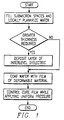
- FIG. 1 A brief flow chart of the method of the present invention is shown in Fig. 1.
- the process begins with the filling of submicron spaces with an interlevel dielectric typically comprising an oxide such as TEOS / O3 although other dielectric materials useful for filling submicron spaces can be used as well.
- the oxide is deposited using any suitable depositing method such as atmospheric or sub-atmospheric chemical vapor deposition(CVD). This will result in filling the submicron spaces in the structure resulting in an upper surface which is locally planarized.
- CVD chemical vapor deposition
- a second dielectric deposition process may be required to produce the desired dielectric thickness and to improve the global planarity.
- an etch back step may also be utilized to minimize the mirroring of underlying structure.
- the etch back and coating process may be repeated.
- the desired surface after these steps is preferably one with an aspect ratio of features of up to about 1.5/1.
- the dielectric used for local planarization should have good properties, such as having high breakdown strength, low dielectric constant, freedom from pinholes, etc, as the dielectric will become part of the final device structure.
- the global planarization is started.
- the wafer is first coated with a film of a deformable (and sacrificial) dielectric such as spun on glass(SOG), a suitable resin or even a glass.
- a deformable (and sacrificial) dielectric such as spun on glass(SOG), a suitable resin or even a glass.
- SOG spun on glass
- All of the mentioned and other useful materials for the deformable film have a characteristic, usually occurring at elevated temperatures, wherein the material is deformable under pressure.
- the uncured deformable film is applied to the wafer, it is maintained at a temperature, usually above typical room temperature, at which deformation is possible.
- the deformable film is then deformed by squeezing the film coated wafer between two ultra-parallel, ultra-flat and temperature controlled bodies.
- an ultra-flat surface is one where the maximum height variation about a mean height is in the order of about 250 A.
- Ultra-parallel implies that the two bodies between which the wafer is squeezed have surfaces which are separated by a distance which varies no more than about 250 A about the mean separation distance.
- the stress in the deformable film exceeds its yield stress, the film will deform to the shape of the plates in contact therewith.
- a pressure of up to about 2 MPa is applied during the squeezing operation, although higher pressure may be required to deform some materials.
- the temperature of the plates may be controlled to achieve a controlled curing of the deformable film.
- the temperature of the plates will be quickly raised at the beginning of the squeezing operation.
- the curing can usually be accelerated by raising the temperature. This will speed the cycle time for the manufacturing process.
- materials such as glass, they becomes deformable at elevated temperature under the applied pressure.
- the pressure may be reduced because if the rate of deformation is too great, the deformable film may crack. Also, reduced pressure may be needed to prevent squeezing most of the deformable film out from contact with one of the plates.
- the temperature of the plates can be lowered so that the wafer can be removed and a new wafer can be loaded into the squeezing apparatus.
- multiple squeeze and release cycles may be required to produce the desired conformity of the film coated surface of the wafer to the surface of the body squeezed against the film.
- an etch may be desired to reduce the thickness of the film to a desired thickness.
- Fig. 2 illustrates an apparatus for squeezing a wafer during the curing of a deformable film.
- the squeezing apparatus is located in a closed chamber 59 and includes an ultra-flat temperature controlled chuck 30 having an upper surface on which a wafer 32 rests.
- the chuck 30 has three vertical holes positioned to permit three load/unload fingers 34 to pass therethrough when desired.
- the fingers 34 are attached to a plate 36 which may be raised or lowered by any suitable mechanism in the direction of the double headed arrow 38. When the fingers 34 are in their lowered position as illustrated in Fig. 2, the wafer 32 will rest on the upper surface of the chuck 30.
- a wafer moving arm (not shown) can project through the opening 39 in the chamber 59, which is normally covered by the door 40 illustrated in its closed position, and lift the wafer 32 off the fingers 34.
- a wafer can be loaded into the assembly of Fig. 2.
- the apparatus of Fig. 2 includes a temperature controlled ultra-flat plate 42 having a lower surface preferable coated with a non-stick material 43 such as a fluro-polymer, e.g. TeflonTM, which prevents the deformable film formed on the upper surface of the wafer 32 from being separated from the wafer when pressure from the plate 42 is withdrawn.
- the plate 42 has three gimbal mounts 44 attached to the upper surface thereof.
- the gimbal mounts 44 are coupled to piezoelectric actuators 51 which are mounted on the lower surface of a plate 46 which may be rotated around the axis 47 or raised and lowered in the direction of double headed arrow 48.
- the gap between the plate 42 and the chuck 30 is monitored by three position sensors 50 (two of which are shown).
- the plate 42 in operation is lowered toward the chuck 30.
- the sensors 50 actuate the piezoelectric actuators 51 coupled thereto to adjust the squeezing pressure applied to the wafer 32 to a desired pressure.
- the above described apparatus may be utilized to produce a surface which is not flat. This is accomplished by having a desired surface topography formed on the lower surface of the plate 42.
- the plate 42 is then rotationally positioned by rotation about the axis 47 and lowered into pressure engagement with the film coated wafer. When this plate is pressed into the uncured deformable film on top of the wafer, the upper surface of the film will conform to the topography of the lower surface of the plate 42.
- Both the chuck 30 and the plate 42 are temperature controlled using conventional temperature control techniques. Both the chuck 30 and plate 42 may have resistive heating elements imbedded therein with external connections to a temperature control circuit for applying controlled electrical power to the heating elements so that chuck 30 and the plate 42 can be heated to a selected elevated temperature. In the alternative, both the chuck 30 and the plate 42 can be heated by a heated fluid which is pumped through fluid passages therein. Indeed, the chuck 30 and the plate 42 can be temperature controlled by both resistive heating elements and by heated fluid being pumped through passages therein. Other controlled heating methods and apparatus can be employed so long as a selectable temperature sufficiently high to cause the dielectric to deform under pressure can be maintained.
- the apparatus described above consists of an assembly disposed inside a closed chamber 59 largely defined by exterior walls 60.
- the door 40 illustrated in its closed position, provides access, when opened, to the closed chamber 59 through opening 39.
- a throttle valve 62 which controls the air pressure inside the chamber 59, is disposed between the chamber 59 defined by the walls 60 and a vacuum pump (not shown) which draws air out of the chamber 59 in the direction of arrow 64.
- a pressure source could be coupled to the throttle valve 62 to admit a gas into the chamber 59 at a desired pressure.
- a film of a deformable dielectric such as spun on glass (SOG) is deposited on the wafer .
- the film material can be deposited on a wafer by various methods, for example, by dripping the film material onto the wafer in a liquid state while the wafer is being spun. The material will quickly flow over the surface of the wafer.
- deformable metal films they may be deposited via sputtering or CVD and typically are selected from the group comprising aluminum, tin or other low melting point metals. At this point, the wafer is ready for the curing process during which the film is flattened.
- the wafer is placed in an apparatus of the type illustrated in Fig. 2.
- the dielectric film is deformed so as to conform to the shape of the plate 42 which is flat.
- the pressure maintained during curing is in the order of 1-10 MPa.
- the pressure maintained during curing will most likely different from that used for spun on glass and the best pressure must be determined by experimentation.
- the curing of the dielectric film is affected by temperature.
- the chuck 30 and the plate 42 in the preferred embodiment of the apparatus, are temperature controlled.
- the temperature of the chuck 30 and the plate 42 will be elevated to about 700 degrees Celsius and will be maintained at that temperature for about two (2) minutes. This elevated temperature is most easily achieved by passing a controlled current through a resistive heating element buried in the chuck 30 and the plate 42 although other approaches for heating the chuck 30 and plate 42 may also be utilized.
- the temperature is thereafter lowered using a liquid coolant which is forced through cooling passages in both the chuck 30 and the plate 42.
- the liquid coolant is utilized to rapidly cool the chuck 30 and plate 42, however, if a slower or different cooling rate is desired, other cooling methods can be used such as radiant cooling, controlled reduction of current through the resistive heating element, or any other method for achieving the desired cooling rate.
- FIG. 3 an alternative embodiment of the apparatus of Fig. 2 is shown.
- the elements of Fig. 2 which are the same as in Fig. 2 have the same lead line designations in Fig. 3 as in Fig. 2.
- the principal difference between the apparatus of Fig.2 and that of Fig. 3 is that in Fig. 2, uniform pressure on the film is provided by the plate 42 being forced into contact with the film on the wafer surface while in Fig. 3, a fluid 70 under high pressure is disposed between plate 72 and the wafer 32 to apply uniform pressure on the film on the wafer 32.
- the apparatus of Fig. 3 includes a pressure plate 72 which is movable up and down in the direction indicated by double headed arrow 74.
- the plate 72 is illustrated schematically in Fig. 3 and comprises a disc shaped body as viewed from above. Plate 72 acts like a piston and is forced downwardly by a motor or other suitable force generating apparatus (not shown) coupled to shaft 73. Downward movement of the plate 72 pressurizes the fluid 70 disposed between the plate 72 and the wafer 32. This will planarize the deformable film and also fill gaps and voids.
- the wafer 32 is maintained at suitable curing temperature by maintaining the plate 30, plate 72 and the fluid 70 at a suitable curing temperature.
- the pressure of the fluid 70 on the upper surface of the coated wafer 32 is maintained during curing in the range described with respect to the apparatus of Fig. 2.
- the fluid 70 may be either a liquid, a gas or a super critical fluid.
- a super critical fluid has properties like a gas at low pressure and properties somewhat between a gas and a liquid at high pressure.
- the fluid 70 is introduced and withdrawn from the cavity between the plate 30 and plate 72 by schematically illustrated conduits 76 and 78.
- the valve 62 and the attached pump 64 serves to evacuate any of the fluid 70 from the apparatus at times when a wafer is being either loaded or unloaded or in the event removal by the conduits 76 and 78 is not as complete as desired.
- the apparatus of Fig. 3 includes a door 80 which seals the opening 82 in the vertical wall 84 which encircles the plates 72 and 30 thereby forming the closed chamber in which the wafer 32 can be subjected to the pressurized fluid 70.
- Suitable pressure sealing rings 86 are disposed between the plate 72 and the wall 84 to prevent the fluid 70, when under pressure, from escaping from the chamber formed between the wall 84 and plates 30 and 72.
- Suitable additional sealing rings may be required between the plate 30 and the wall 84 if it is desired not to fill the chamber 88 located below the plate 30 and the exterior wall 90 of the apparatus. In this alternative, seals may also be required between the posts 34 and the plate 30.
- the wafer 32 is loaded and unloaded from the apparatus of Fig. 3 in a manner similar to that of Fig. 2.
- the atmosphere within the apparatus is first adjusted to that of the environment outside door 40.
- both door 40 and door 80 are opened.
- the posts 34 are raised to lift the wafer 32 above the plate 30 and an external arm (not shown) enters the chamber and lifts the wafer 32 off the posts 34.
- the wafer 32 is withdrawn and another introduced for planarization.
Landscapes
- Engineering & Computer Science (AREA)
- Physics & Mathematics (AREA)
- Condensed Matter Physics & Semiconductors (AREA)
- General Physics & Mathematics (AREA)
- Manufacturing & Machinery (AREA)
- Computer Hardware Design (AREA)
- Microelectronics & Electronic Packaging (AREA)
- Power Engineering (AREA)
- Mechanical Engineering (AREA)
- Internal Circuitry In Semiconductor Integrated Circuit Devices (AREA)
- Formation Of Insulating Films (AREA)
Abstract
Description
- This invention relates generally to the field of planarizing semiconductor wafers and specifically to the field of global planarizing the surface of a wafer to produce a flat surface on which interconnect wiring can be formed.
- The advent of multi-level metallization in ULSI circuits has placed stringent requirements on the planarity of the surface prior to metallization. Indeed, without some form of planarization between intervening layers of metallization, the topography of the lower layers is to some extent reflected in the topography of the insulating layer which forms the surface on which each additional level of metallization is formed. This is undesirable because it adds to the processing steps required and can lead to reduced device reliability.
- There are two types of planarization which must be achieved; local and global. In local planarization, spaces between closely packed features are filled with an interlevel dielectric. Ideally, the dielectric provides void free filling and a locally planarized surface. In reality, however, the surface of the filled areas still reflect some of the underlying topography. When large areas of the wafer have been covered by an interlevel dielectric and there are no isolated features present, global planarization is achieved. Because the requirements of these two types of planarization are so different, separate processes are employed. Usually, local planarization is performed first followed by global planarization.
- A number of local planarization processes are known and have proved successful. One such process involves atmospheric pressure chemical vapor deposition (APCVD) and sub-atmospheric chemical vapor deposition (SACVD) of TEOS and O₃. These processes provide void-free filling of submicron spaces, with a relatively planar TEOS oxide film but global planarization cannot be achieved. The films provide good electrical characteristics in that the film has a high breakdown strength, is free of pin holes and has a low dielectric constant. The film also becomes a part of the device structure.
- Local planarization, though somewhat defective, can also be achieved with electron cyclotron resonance (ECR) deposited oxide films, however, the upper surface topology mirrors that of the underlying features. Other problems with this approach include safety concerns about high bias voltages being used during deposition and unacceptable defect frequency. The films produced, however, have good electrical properties and become part of the device structure.
- A third approach for local planarization involves low pressure chemical vapor deposition (LPCVD) or plasma enhanced chemical vapor deposition (PECVD) TEOS oxide followed by deposition and reflow of boro phospho silicate glass (BPSG). This process is suitable for local planarization but it has not proved to be suitable for complete global planarization.
- A fourth approach involves conventional sputter deposition of aluminum which produces planar films that form the interconnect. Step coverage of the film in contacts/vias, however, is poor thereby leading to incomplete filling. For this reason, CVD tungsten, which has good gap filling properties due to its highly conformal nature, is used fill the contacts/vias, while aluminum is used to form the interconnect. However, this process sequence is complicated, and a single aluminum deposition to form the contact/via plugs and the interconnect is preferred. Recently, aluminum reflow that employs high temperature aluminum deposition to improve the step coverage has been demonstrated for void-free contact/via filling. However, this method is sensitive to the surface state of the wafer and does not reliably fill contacts/vias.
- Local planarization is often followed by one of the global planarization techniques. One of the most common approaches involves coating the surface with a sacrificial dielectric followed by an etchback. This includes schemes such as SOG etchback and resist etchback, in which the wafer is coated with the dielectric. Because of the low surface tension of the dielectric during the coating process, the dielectric tends to flow into lower areas which, on curing, forms a film that reduces the severity of the underlying topography. This reduced severity of topography is then transferred into the underlying dielectric (usually an oxide) via an etchback in which the sacrificial dielectric is removed. By repeating this cycle several times, a planarized surface is obtained. The biggest disadvantage of this process is the multiple coating and etchback cycles required to obtain acceptable planarization. Often more than four cycles are required for adequate planarization.
- To reduce the number of cycles required, blocking masks can be used, in which the sacrificial dielectric is coated and then patterned so that it fills up the dips in the topography. Another coat of the sacrificial dielectric is then applied to produce a planarized surface. This planar topography is transferred to the underlying interlevel dielectric via an etchback.
- Another global planarizing approach that has gained some popularity is known as chemical mechanical polishing. In this technique, a polishing pad is used with a reactive slurry to polish the wafer surface until the surface is planarized. This technique, however, suffers from several limitations. The polishing rates are a function of many variables including feature size, aspect ratio, feature density and material type. Polishing rates also vary across the wafer and depend on the quality of the polishing pad. When carefully applied, however, this technique has proved successful.
- There are other approaches which are still in the experimental stage and involve new spin on or deposited dielectrics that provide good gap filling, electrical and thermal properties, and also provide global planarization. Examples of these materials include various types of fluorinated polymers, polyimides and siloxanes. All these approaches increase the planarization scale lengths appreciable (>100 µm), but still do not provide true global planarization.
- The present invention seeks to overcome the above outlined problems related to global planarization of a wafer. The first step of the method involves using well developed techniques to achieve high quality filling of submicron spaces with an interlevel dielectric which results in producing a locally planarized surface. In some instances, a second film of interlevel dielectric may be deposited on the wafer to produce the desired interlevel thickness and improve global planarity. Thereafter, the wafer is coated with a deformable (and sacrificial) dielectric. This film is mechanically deformed during a controlled cure by squeezing the wafer between two temperature controlled, ultra-flat and ultra-parallel plates. After curing, the dielectric film has a flat surface on which a layer of metalization or any other structure can be formed.
-
- Fig. 1 is a brief flow chart illustrating the planarization method of this invention;
- Fig. 2 is a schematic diagram of the apparatus used in the method of this invention for squeezing a wafer with a deformable dielectric film during curing of the dielectric material.
- Fig. 3 is a schematic diagram of an alternative apparatus used in the method of this invention for applying uniform pressure to a deformable film being planarized on the surface of a wafer.
- A brief flow chart of the method of the present invention is shown in Fig. 1. The process begins with the filling of submicron spaces with an interlevel dielectric typically comprising an oxide such as TEOS / O₃ although other dielectric materials useful for filling submicron spaces can be used as well. The oxide is deposited using any suitable depositing method such as atmospheric or sub-atmospheric chemical vapor deposition(CVD). This will result in filling the submicron spaces in the structure resulting in an upper surface which is locally planarized. In some instances, a second dielectric deposition process may be required to produce the desired dielectric thickness and to improve the global planarity. As the coating will frequently have a topography which mirrors the underlying structure, an etch back step may also be utilized to minimize the mirroring of underlying structure. The etch back and coating process may be repeated. The desired surface after these steps is preferably one with an aspect ratio of features of up to about 1.5/1.
- The dielectric used for local planarization should have good properties, such as having high breakdown strength, low dielectric constant, freedom from pinholes, etc, as the dielectric will become part of the final device structure.
- Once the dielectric has reached the desired thickness and local planarization achieved, the global planarization is started. During global planarization, the wafer is first coated with a film of a deformable (and sacrificial) dielectric such as spun on glass(SOG), a suitable resin or even a glass. All of the mentioned and other useful materials for the deformable film have a characteristic, usually occurring at elevated temperatures, wherein the material is deformable under pressure.
- Once the uncured deformable film is applied to the wafer, it is maintained at a temperature, usually above typical room temperature, at which deformation is possible. The deformable film is then deformed by squeezing the film coated wafer between two ultra-parallel, ultra-flat and temperature controlled bodies. In this context, an ultra-flat surface is one where the maximum height variation about a mean height is in the order of about 250 A. Ultra-parallel implies that the two bodies between which the wafer is squeezed have surfaces which are separated by a distance which varies no more than about 250 A about the mean separation distance. When the stress in the deformable film exceeds its yield stress, the film will deform to the shape of the plates in contact therewith. In practice, a pressure of up to about 2 MPa is applied during the squeezing operation, although higher pressure may be required to deform some materials.
- The temperature of the plates may be controlled to achieve a controlled curing of the deformable film. Typically, the temperature of the plates will be quickly raised at the beginning of the squeezing operation. In the case where the deformable film cures chemically, the curing can usually be accelerated by raising the temperature. This will speed the cycle time for the manufacturing process. For materials such as glass, they becomes deformable at elevated temperature under the applied pressure. When the material becomes deformable, however, the pressure may be reduced because if the rate of deformation is too great, the deformable film may crack. Also, reduced pressure may be needed to prevent squeezing most of the deformable film out from contact with one of the plates. Once the deformable film has cured, the temperature of the plates can be lowered so that the wafer can be removed and a new wafer can be loaded into the squeezing apparatus.
- In some cases, multiple squeeze and release cycles may be required to produce the desired conformity of the film coated surface of the wafer to the surface of the body squeezed against the film. In addition, on completion of the squeezing step(s), in some cases an etch may be desired to reduce the thickness of the film to a desired thickness.
- Fig. 2 illustrates an apparatus for squeezing a wafer during the curing of a deformable film. The squeezing apparatus is located in a
closed chamber 59 and includes an ultra-flat temperature controlledchuck 30 having an upper surface on which awafer 32 rests. Thechuck 30 has three vertical holes positioned to permit three load/unloadfingers 34 to pass therethrough when desired. Thefingers 34 are attached to aplate 36 which may be raised or lowered by any suitable mechanism in the direction of the double headedarrow 38. When thefingers 34 are in their lowered position as illustrated in Fig. 2, thewafer 32 will rest on the upper surface of thechuck 30. However, when theplate 36 is raised (not illustrated), all thefingers 34 extend through the upper surface of thechuck 30 and support thewafer 32 from below at a position above the upper surface of thechuck 30. While thewafer 32 is so supported by thefingers 34, a wafer moving arm (not shown) can project through theopening 39 in thechamber 59, which is normally covered by thedoor 40 illustrated in its closed position, and lift thewafer 32 off thefingers 34. In a similar fashion, a wafer can be loaded into the assembly of Fig. 2. - The apparatus of Fig. 2 includes a temperature controlled
ultra-flat plate 42 having a lower surface preferable coated with anon-stick material 43 such as a fluro-polymer, e.g. Teflon™, which prevents the deformable film formed on the upper surface of thewafer 32 from being separated from the wafer when pressure from theplate 42 is withdrawn. Theplate 42 has three gimbal mounts 44 attached to the upper surface thereof. The gimbal mounts 44 are coupled topiezoelectric actuators 51 which are mounted on the lower surface of aplate 46 which may be rotated around theaxis 47 or raised and lowered in the direction of double headedarrow 48. The gap between theplate 42 and thechuck 30 is monitored by three position sensors 50 (two of which are shown). Theplate 42 in operation is lowered toward thechuck 30. When theplate 42 is a desired distance above thechuck 30, thesensors 50 actuate thepiezoelectric actuators 51 coupled thereto to adjust the squeezing pressure applied to thewafer 32 to a desired pressure. - While the preferred embodiment of the invention is to have a
flat plate 42 come in contact with the deformable film on a wafer so as to produce a flat surface on the film, the above described apparatus may be utilized to produce a surface which is not flat. This is accomplished by having a desired surface topography formed on the lower surface of theplate 42. Theplate 42 is then rotationally positioned by rotation about theaxis 47 and lowered into pressure engagement with the film coated wafer. When this plate is pressed into the uncured deformable film on top of the wafer, the upper surface of the film will conform to the topography of the lower surface of theplate 42. - Both the
chuck 30 and theplate 42 are temperature controlled using conventional temperature control techniques. Both thechuck 30 andplate 42 may have resistive heating elements imbedded therein with external connections to a temperature control circuit for applying controlled electrical power to the heating elements so thatchuck 30 and theplate 42 can be heated to a selected elevated temperature. In the alternative, both thechuck 30 and theplate 42 can be heated by a heated fluid which is pumped through fluid passages therein. Indeed, thechuck 30 and theplate 42 can be temperature controlled by both resistive heating elements and by heated fluid being pumped through passages therein. Other controlled heating methods and apparatus can be employed so long as a selectable temperature sufficiently high to cause the dielectric to deform under pressure can be maintained. - The apparatus described above consists of an assembly disposed inside a
closed chamber 59 largely defined byexterior walls 60. Thedoor 40, illustrated in its closed position, provides access, when opened, to theclosed chamber 59 throughopening 39. Athrottle valve 62, which controls the air pressure inside thechamber 59, is disposed between thechamber 59 defined by thewalls 60 and a vacuum pump (not shown) which draws air out of thechamber 59 in the direction ofarrow 64. This allows the equipment operator to select the desired pressure within thechamber 59 for curing of the deformable film in an ambient which is sub-atmospheric. Conversely, if it were deemed desirable to perform the curing of the dielectric film at pressures above atmospheric pressure, a pressure source could be coupled to thethrottle valve 62 to admit a gas into thechamber 59 at a desired pressure. - Once the surface of the wafer has been locally planarized, a film of a deformable dielectric, such as spun on glass (SOG), is deposited on the wafer . The film material can be deposited on a wafer by various methods, for example, by dripping the film material onto the wafer in a liquid state while the wafer is being spun. The material will quickly flow over the surface of the wafer. In the case of deformable metal films, they may be deposited via sputtering or CVD and typically are selected from the group comprising aluminum, tin or other low melting point metals. At this point, the wafer is ready for the curing process during which the film is flattened.
- During the curing of the film, the wafer is placed in an apparatus of the type illustrated in Fig. 2. By squeezing the wafer with an uncured dielectric film thereon between the
plate 42 and thechuck 30, the dielectric film is deformed so as to conform to the shape of theplate 42 which is flat. During this squeezing process for a dielectric such as spun on glass, the pressure maintained during curing is in the order of 1-10 MPa. For other dielectrics, the pressure maintained during curing will most likely different from that used for spun on glass and the best pressure must be determined by experimentation. Once the dielectric film is cured, the upper surface thereof will be flat as it has confirmed to the shape of theplate 42 during the curing. - The curing of the dielectric film is affected by temperature. Hence, the
chuck 30 and theplate 42, in the preferred embodiment of the apparatus, are temperature controlled. During the curing of a film made of SOG, for example, the temperature of thechuck 30 and theplate 42 will be elevated to about 700 degrees Celsius and will be maintained at that temperature for about two (2) minutes. This elevated temperature is most easily achieved by passing a controlled current through a resistive heating element buried in thechuck 30 and theplate 42 although other approaches for heating thechuck 30 andplate 42 may also be utilized. The temperature is thereafter lowered using a liquid coolant which is forced through cooling passages in both thechuck 30 and theplate 42. The liquid coolant is utilized to rapidly cool thechuck 30 andplate 42, however, if a slower or different cooling rate is desired, other cooling methods can be used such as radiant cooling, controlled reduction of current through the resistive heating element, or any other method for achieving the desired cooling rate. - Referring now to Fig. 3, an alternative embodiment of the apparatus of Fig. 2 is shown. In this drawing, the elements of Fig. 2 which are the same as in Fig. 2 have the same lead line designations in Fig. 3 as in Fig. 2. The principal difference between the apparatus of Fig.2 and that of Fig. 3 is that in Fig. 2, uniform pressure on the film is provided by the
plate 42 being forced into contact with the film on the wafer surface while in Fig. 3, a fluid 70 under high pressure is disposed betweenplate 72 and thewafer 32 to apply uniform pressure on the film on thewafer 32. - The apparatus of Fig. 3 includes a
pressure plate 72 which is movable up and down in the direction indicated by double headedarrow 74. Theplate 72 is illustrated schematically in Fig. 3 and comprises a disc shaped body as viewed from above.Plate 72 acts like a piston and is forced downwardly by a motor or other suitable force generating apparatus (not shown) coupled toshaft 73. Downward movement of theplate 72 pressurizes the fluid 70 disposed between theplate 72 and thewafer 32. This will planarize the deformable film and also fill gaps and voids. As with the apparatus of Fig. 2, thewafer 32 is maintained at suitable curing temperature by maintaining theplate 30,plate 72 and the fluid 70 at a suitable curing temperature. The pressure of the fluid 70 on the upper surface of thecoated wafer 32 is maintained during curing in the range described with respect to the apparatus of Fig. 2. - The fluid 70 may be either a liquid, a gas or a super critical fluid. A super critical fluid has properties like a gas at low pressure and properties somewhat between a gas and a liquid at high pressure. The fluid 70 is introduced and withdrawn from the cavity between the
plate 30 andplate 72 by schematically illustratedconduits valve 62 and the attachedpump 64 serves to evacuate any of the fluid 70 from the apparatus at times when a wafer is being either loaded or unloaded or in the event removal by theconduits - The apparatus of Fig. 3 includes a
door 80 which seals theopening 82 in thevertical wall 84 which encircles theplates wafer 32 can be subjected to thepressurized fluid 70. Suitable pressure sealing rings 86 are disposed between theplate 72 and thewall 84 to prevent the fluid 70, when under pressure, from escaping from the chamber formed between thewall 84 andplates plate 30 and thewall 84 if it is desired not to fill thechamber 88 located below theplate 30 and theexterior wall 90 of the apparatus. In this alternative, seals may also be required between theposts 34 and theplate 30. - The
wafer 32 is loaded and unloaded from the apparatus of Fig. 3 in a manner similar to that of Fig. 2. The atmosphere within the apparatus is first adjusted to that of the environment outsidedoor 40. Then bothdoor 40 anddoor 80 are opened. Theposts 34 are raised to lift thewafer 32 above theplate 30 and an external arm (not shown) enters the chamber and lifts thewafer 32 off theposts 34. Thereafter, thewafer 32 is withdrawn and another introduced for planarization. - While the above description has been directed to the embodiment of the present invention as illustrated in the Figures, those of skill in the art will recognize that the specific illustrated embodiment may be modified in many ways as outlined above and in other ways as well without departing from the spirit and scope of the present invention as defined by the following claims.
Claims (13)
- A method for global planarization of a surface of a semiconductor wafer comprising the steps of:
coating the wafer with a deformable film; and
adjusting a control parameter to effect deformation of said film to produce a planar surface. - The method of Claim 1, further comprising forming the wafer having features thereon; filling the spaces between the features with an interlevel dielectric material.
- The method of Claim 1 or Claim 2, further comprising forming said interlevel dielectric as a material for filling submicron spaces between features formed on said wafer.
- The method of Claim 2 or Claim 3, further comprising forming said deformable film as a material which deforms at an elevated temperature and pressure.
- The method of any preceding Claim, additionally including the step of maintaining said deformable film at a temperature at which said deformable film can be deformed under the control parameter.
- The method of any preceding claim, further comprising the steps of:
controlling the temperature of two bodies having substantially planar and parallel surfaces; and
squeezing said wafer between said parallel surfaces to deform said film to produce a planar surface thereon. - The method of Claim 6, additionally including the step of continuing to squeeze said wafer until said deformable film has cured.
- The method of Claim 6 or Claim 7, wherein said controlling step includes elevating the temperature of said deformable film prior to curing thereof and reducing the temperature once said deformable film is cured.
- The method of Claim 2 or any of Claims 3 to 8 when dependent on Claim 2, wherein said filling step comprises producing an aspect ratio of features on the wafer of no greater than about 1.5/1.
- The method of any preceding Claim, further comprising selecting said deformable film from the group consisting of spun on glass, low melting point metals, low melting point alloys, resins and reflowable glass.
- The method of any preceding claim, wherein the adjusting step comprises adjusting the temperature and or the pressure of the deformable film to effect said deformation.
- An apparatus for producing a surface of a semiconductor wafer which conforms to a desired topography comprising, in combination:
means for supporting a semiconductor wafer coated with a deformable film material, said means for supporting having a substantially planar surface on which said wafer rests; and
means for controlling a parameter to produce a planar surface on the coated wafer. - The apparatus of Claim 12, additionally including means for controlling the temperature and pressure of said plate and said means for supporting.
Applications Claiming Priority (2)
| Application Number | Priority Date | Filing Date | Title |
|---|---|---|---|
| US188498 | 1994-01-28 | ||
| US08/188,498 US5434107A (en) | 1994-01-28 | 1994-01-28 | Method for planarization |
Publications (2)
| Publication Number | Publication Date |
|---|---|
| EP0665580A2 true EP0665580A2 (en) | 1995-08-02 |
| EP0665580A3 EP0665580A3 (en) | 1997-03-05 |
Family
ID=22693403
Family Applications (1)
| Application Number | Title | Priority Date | Filing Date |
|---|---|---|---|
| EP95100971A Withdrawn EP0665580A3 (en) | 1994-01-28 | 1995-01-25 | Method and apparatus for global planarisation of a surface of a semiconductor wafer. |
Country Status (5)
| Country | Link |
|---|---|
| US (1) | US5434107A (en) |
| EP (1) | EP0665580A3 (en) |
| JP (1) | JPH0817812A (en) |
| KR (1) | KR950034586A (en) |
| TW (1) | TW299483B (en) |
Cited By (2)
| Publication number | Priority date | Publication date | Assignee | Title |
|---|---|---|---|---|
| EP1440465A1 (en) * | 2001-10-31 | 2004-07-28 | Brewer Science, Inc. | Contact planarization materials that generate no volatile byproducts or residue during curing |
| EP3637456A3 (en) * | 2018-10-11 | 2020-12-16 | Canon Kabushiki Kaisha | Film forming apparatus, film forming method, and method of manufacturing article |
Families Citing this family (78)
| Publication number | Priority date | Publication date | Assignee | Title |
|---|---|---|---|---|
| US5736424A (en) * | 1987-02-27 | 1998-04-07 | Lucent Technologies Inc. | Device fabrication involving planarization |
| US5679610A (en) * | 1994-12-15 | 1997-10-21 | Kabushiki Kaisha Toshiba | Method of planarizing a semiconductor workpiece surface |
| TW291589B (en) * | 1995-03-30 | 1996-11-21 | Ftl Co Ltd | |
| US5679211A (en) * | 1995-09-18 | 1997-10-21 | Taiwan Semiconductor Manufacturing Company, Ltd. | Spin-on-glass etchback planarization process using an oxygen plasma to remove an etchback polymer residue |
| US20040137734A1 (en) * | 1995-11-15 | 2004-07-15 | Princeton University | Compositions and processes for nanoimprinting |
| US6518189B1 (en) * | 1995-11-15 | 2003-02-11 | Regents Of The University Of Minnesota | Method and apparatus for high density nanostructures |
| US7758794B2 (en) * | 2001-10-29 | 2010-07-20 | Princeton University | Method of making an article comprising nanoscale patterns with reduced edge roughness |
| US6309580B1 (en) * | 1995-11-15 | 2001-10-30 | Regents Of The University Of Minnesota | Release surfaces, particularly for use in nanoimprint lithography |
| US20040036201A1 (en) * | 2000-07-18 | 2004-02-26 | Princeton University | Methods and apparatus of field-induced pressure imprint lithography |
| US5967030A (en) | 1995-11-17 | 1999-10-19 | Micron Technology, Inc. | Global planarization method and apparatus |
| US6413870B1 (en) | 1996-09-30 | 2002-07-02 | International Business Machines Corporation | Process of removing CMP scratches by BPSG reflow and integrated circuit chip formed thereby |
| US5848615A (en) * | 1996-12-04 | 1998-12-15 | Ingersoll-Rand Company | Check valve cartridge for fluid pump |
| US6331488B1 (en) * | 1997-05-23 | 2001-12-18 | Micron Technology, Inc. | Planarization process for semiconductor substrates |
| US6316363B1 (en) | 1999-09-02 | 2001-11-13 | Micron Technology, Inc. | Deadhesion method and mechanism for wafer processing |
| GB9714531D0 (en) * | 1997-07-11 | 1997-09-17 | Trikon Equip Ltd | Forming a layer |
| US6060386A (en) * | 1997-08-21 | 2000-05-09 | Micron Technology, Inc. | Method and apparatus for forming features in holes, trenches and other voids in the manufacturing of microelectronic devices |
| US6103638A (en) * | 1997-11-07 | 2000-08-15 | Micron Technology, Inc. | Formation of planar dielectric layers using liquid interfaces |
| EP0948035A1 (en) * | 1998-03-19 | 1999-10-06 | Applied Materials, Inc. | Method for applying a dielectric cap film to a dielectric stack |
| US6036586A (en) * | 1998-07-29 | 2000-03-14 | Micron Technology, Inc. | Apparatus and method for reducing removal forces for CMP pads |
| JP3337464B2 (en) * | 1998-08-31 | 2002-10-21 | 日立化成工業株式会社 | Polishing liquid for metal and polishing method |
| US20020001947A1 (en) | 1998-09-02 | 2002-01-03 | David A. Cathey | Semiconductor processing method using high pressure liquid media treatment |
| US6642140B1 (en) | 1998-09-03 | 2003-11-04 | Micron Technology, Inc. | System for filling openings in semiconductor products |
| US6218316B1 (en) | 1998-10-22 | 2001-04-17 | Micron Technology, Inc. | Planarization of non-planar surfaces in device fabrication |
| JP3832142B2 (en) | 1999-06-24 | 2006-10-11 | 株式会社日立製作所 | Pipe thickness reduction management system |
| US6589889B2 (en) * | 1999-09-09 | 2003-07-08 | Alliedsignal Inc. | Contact planarization using nanoporous silica materials |
| WO2001018860A2 (en) * | 1999-09-09 | 2001-03-15 | Alliedsignal Inc. | Improved apparatus and methods for integrated circuit planarization |
| US6165911A (en) * | 1999-12-29 | 2000-12-26 | Calveley; Peter Braden | Method of patterning a metal layer |
| DE10022656B4 (en) * | 2000-04-28 | 2006-07-06 | Infineon Technologies Ag | Method for removing structures |
| US7211214B2 (en) * | 2000-07-18 | 2007-05-01 | Princeton University | Laser assisted direct imprint lithography |
| WO2002009147A2 (en) * | 2000-07-26 | 2002-01-31 | Tokyo Electron Limited | High pressure processing chamber for semiconductor substrate |
| US6518172B1 (en) | 2000-08-29 | 2003-02-11 | Micron Technology, Inc. | Method for applying uniform pressurized film across wafer |
| JP3927768B2 (en) * | 2000-11-17 | 2007-06-13 | 松下電器産業株式会社 | Manufacturing method of semiconductor device |
| TW513736B (en) * | 2001-05-04 | 2002-12-11 | Chartered Semiconductor Mfg | Thermal mechanical planarization in integrated circuits |
| US20030080472A1 (en) * | 2001-10-29 | 2003-05-01 | Chou Stephen Y. | Lithographic method with bonded release layer for molding small patterns |
| US7455955B2 (en) * | 2002-02-27 | 2008-11-25 | Brewer Science Inc. | Planarization method for multi-layer lithography processing |
| US7387868B2 (en) * | 2002-03-04 | 2008-06-17 | Tokyo Electron Limited | Treatment of a dielectric layer using supercritical CO2 |
| US7077992B2 (en) | 2002-07-11 | 2006-07-18 | Molecular Imprints, Inc. | Step and repeat imprint lithography processes |
| US6932934B2 (en) | 2002-07-11 | 2005-08-23 | Molecular Imprints, Inc. | Formation of discontinuous films during an imprint lithography process |
| US8349241B2 (en) | 2002-10-04 | 2013-01-08 | Molecular Imprints, Inc. | Method to arrange features on a substrate to replicate features having minimal dimensional variability |
| US7225820B2 (en) * | 2003-02-10 | 2007-06-05 | Tokyo Electron Limited | High-pressure processing chamber for a semiconductor wafer |
| US7186656B2 (en) * | 2004-05-21 | 2007-03-06 | Molecular Imprints, Inc. | Method of forming a recessed structure employing a reverse tone process |
| US7179396B2 (en) | 2003-03-25 | 2007-02-20 | Molecular Imprints, Inc. | Positive tone bi-layer imprint lithography method |
| US7323417B2 (en) * | 2004-09-21 | 2008-01-29 | Molecular Imprints, Inc. | Method of forming a recessed structure employing a reverse tone process |
| US7396475B2 (en) | 2003-04-25 | 2008-07-08 | Molecular Imprints, Inc. | Method of forming stepped structures employing imprint lithography |
| US7270137B2 (en) | 2003-04-28 | 2007-09-18 | Tokyo Electron Limited | Apparatus and method of securing a workpiece during high-pressure processing |
| US7790231B2 (en) * | 2003-07-10 | 2010-09-07 | Brewer Science Inc. | Automated process and apparatus for planarization of topographical surfaces |
| US7163380B2 (en) * | 2003-07-29 | 2007-01-16 | Tokyo Electron Limited | Control of fluid flow in the processing of an object with a fluid |
| US20050067002A1 (en) * | 2003-09-25 | 2005-03-31 | Supercritical Systems, Inc. | Processing chamber including a circulation loop integrally formed in a chamber housing |
| US7547504B2 (en) | 2004-09-21 | 2009-06-16 | Molecular Imprints, Inc. | Pattern reversal employing thick residual layers |
| US7241395B2 (en) * | 2004-09-21 | 2007-07-10 | Molecular Imprints, Inc. | Reverse tone patterning on surfaces having planarity perturbations |
| US7205244B2 (en) * | 2004-09-21 | 2007-04-17 | Molecular Imprints | Patterning substrates employing multi-film layers defining etch-differential interfaces |
| US7252777B2 (en) * | 2004-09-21 | 2007-08-07 | Molecular Imprints, Inc. | Method of forming an in-situ recessed structure |
| US7041604B2 (en) * | 2004-09-21 | 2006-05-09 | Molecular Imprints, Inc. | Method of patterning surfaces while providing greater control of recess anisotropy |
| US20060102282A1 (en) * | 2004-11-15 | 2006-05-18 | Supercritical Systems, Inc. | Method and apparatus for selectively filtering residue from a processing chamber |
| US7357876B2 (en) * | 2004-12-01 | 2008-04-15 | Molecular Imprints, Inc. | Eliminating printability of sub-resolution defects in imprint lithography |
| US7767145B2 (en) * | 2005-03-28 | 2010-08-03 | Toyko Electron Limited | High pressure fourier transform infrared cell |
| US20060225772A1 (en) * | 2005-03-29 | 2006-10-12 | Jones William D | Controlled pressure differential in a high-pressure processing chamber |
| US20060226117A1 (en) * | 2005-03-29 | 2006-10-12 | Bertram Ronald T | Phase change based heating element system and method |
| US20060225769A1 (en) * | 2005-03-30 | 2006-10-12 | Gentaro Goshi | Isothermal control of a process chamber |
| US7494107B2 (en) * | 2005-03-30 | 2009-02-24 | Supercritical Systems, Inc. | Gate valve for plus-atmospheric pressure semiconductor process vessels |
| US7256131B2 (en) * | 2005-07-19 | 2007-08-14 | Molecular Imprints, Inc. | Method of controlling the critical dimension of structures formed on a substrate |
| US7259102B2 (en) * | 2005-09-30 | 2007-08-21 | Molecular Imprints, Inc. | Etching technique to planarize a multi-layer structure |
| US7906058B2 (en) * | 2005-12-01 | 2011-03-15 | Molecular Imprints, Inc. | Bifurcated contact printing technique |
| US7803308B2 (en) | 2005-12-01 | 2010-09-28 | Molecular Imprints, Inc. | Technique for separating a mold from solidified imprinting material |
| WO2007067488A2 (en) | 2005-12-08 | 2007-06-14 | Molecular Imprints, Inc. | Method and system for double-sided patterning of substrates |
| US7670530B2 (en) | 2006-01-20 | 2010-03-02 | Molecular Imprints, Inc. | Patterning substrates employing multiple chucks |
| US8850980B2 (en) | 2006-04-03 | 2014-10-07 | Canon Nanotechnologies, Inc. | Tessellated patterns in imprint lithography |
| TW200801794A (en) * | 2006-04-03 | 2008-01-01 | Molecular Imprints Inc | Method of concurrently patterning a substrate having a plurality of fields and a plurality of alignment marks |
| US8142850B2 (en) | 2006-04-03 | 2012-03-27 | Molecular Imprints, Inc. | Patterning a plurality of fields on a substrate to compensate for differing evaporation times |
| US7802978B2 (en) | 2006-04-03 | 2010-09-28 | Molecular Imprints, Inc. | Imprinting of partial fields at the edge of the wafer |
| US8012395B2 (en) | 2006-04-18 | 2011-09-06 | Molecular Imprints, Inc. | Template having alignment marks formed of contrast material |
| US7547398B2 (en) | 2006-04-18 | 2009-06-16 | Molecular Imprints, Inc. | Self-aligned process for fabricating imprint templates containing variously etched features |
| US7775785B2 (en) * | 2006-12-20 | 2010-08-17 | Brewer Science Inc. | Contact planarization apparatus |
| JP4754595B2 (en) * | 2008-03-05 | 2011-08-24 | 大日本スクリーン製造株式会社 | Thin film forming apparatus and method |
| US8865599B2 (en) * | 2011-11-08 | 2014-10-21 | Brewer Science Inc. | Self-leveling planarization materials for microelectronic topography |
| JP2013163846A (en) * | 2012-02-10 | 2013-08-22 | Denso Corp | Film deposition apparatus and film deposition method |
| TWM473078U (en) | 2013-10-07 | 2014-03-01 | Lin Chen Ind Co Ltd | Pants formed with same fabric |
| JP7129315B2 (en) * | 2018-11-05 | 2022-09-01 | キヤノン株式会社 | Flattening layer forming apparatus, flattening method, and article manufacturing method |
Citations (5)
| Publication number | Priority date | Publication date | Assignee | Title |
|---|---|---|---|---|
| JPS6245032A (en) * | 1985-08-22 | 1987-02-27 | Nec Corp | Manufacture of semiconductor device |
| JPS6245045A (en) * | 1985-08-22 | 1987-02-27 | Nec Corp | Manufacture of semiconductor device |
| EP0430040A2 (en) * | 1989-11-27 | 1991-06-05 | Micron Technology, Inc. | Method of forming a conductive via plug or an interconnect line of ductile metal within an integrated circuit using mechanical smearing |
| JPH0574749A (en) * | 1991-09-13 | 1993-03-26 | Toshiro Doi | Method and apparatus for planarization polishing of wafer with device |
| WO1995011521A1 (en) * | 1993-10-23 | 1995-04-27 | Christopher David Dobson | Method and apparatus for the planarization of layers on semiconductor substrates |
Family Cites Families (7)
| Publication number | Priority date | Publication date | Assignee | Title |
|---|---|---|---|---|
| US4894706A (en) * | 1985-02-14 | 1990-01-16 | Nippon Telegraph And Telephone Corporation | Three-dimensional packaging of semiconductor device chips |
| GB2212332A (en) * | 1987-11-11 | 1989-07-19 | Gen Electric Co Plc | Fabrication of electrical circuits |
| US5073518A (en) * | 1989-11-27 | 1991-12-17 | Micron Technology, Inc. | Process to mechanically and plastically deform solid ductile metal to fill contacts of conductive channels with ductile metal and process for dry polishing excess metal from a semiconductor wafer |
| DE69219529T2 (en) * | 1991-08-06 | 1997-12-11 | Nec Corp | Method of applying a metal or passivation layer with high adhesion over an insulated semiconductor substrate |
| US5326243A (en) * | 1992-06-25 | 1994-07-05 | Fierkens Richard H J | Compression-cavity mold for plastic encapsulation of thin-package integrated circuit device |
| US5348615A (en) * | 1992-10-21 | 1994-09-20 | Advanced Micro Devices, Inc. | Selective planarization method using regelation |
| US5302233A (en) * | 1993-03-19 | 1994-04-12 | Micron Semiconductor, Inc. | Method for shaping features of a semiconductor structure using chemical mechanical planarization (CMP) |
-
1994
- 1994-01-28 US US08/188,498 patent/US5434107A/en not_active Expired - Lifetime
-
1995
- 1995-01-25 EP EP95100971A patent/EP0665580A3/en not_active Withdrawn
- 1995-01-27 KR KR1019950001501A patent/KR950034586A/en not_active Application Discontinuation
- 1995-01-30 JP JP7013038A patent/JPH0817812A/en active Pending
- 1995-03-09 TW TW084102223A patent/TW299483B/zh not_active IP Right Cessation
Patent Citations (5)
| Publication number | Priority date | Publication date | Assignee | Title |
|---|---|---|---|---|
| JPS6245032A (en) * | 1985-08-22 | 1987-02-27 | Nec Corp | Manufacture of semiconductor device |
| JPS6245045A (en) * | 1985-08-22 | 1987-02-27 | Nec Corp | Manufacture of semiconductor device |
| EP0430040A2 (en) * | 1989-11-27 | 1991-06-05 | Micron Technology, Inc. | Method of forming a conductive via plug or an interconnect line of ductile metal within an integrated circuit using mechanical smearing |
| JPH0574749A (en) * | 1991-09-13 | 1993-03-26 | Toshiro Doi | Method and apparatus for planarization polishing of wafer with device |
| WO1995011521A1 (en) * | 1993-10-23 | 1995-04-27 | Christopher David Dobson | Method and apparatus for the planarization of layers on semiconductor substrates |
Non-Patent Citations (6)
| Title |
|---|
| IBM TECHNICAL DISCLOSURE BULLETIN, vol. 27, no. 1B, 1 June 1984, NEW YORK, US, page 591/592 XP000563215 DILL F H: "PLANARIZATION LAYERS" * |
| IBM TECHNICAL DISCLOSURE BULLETIN, vol. 32, no. 5A, October 1989, NEW YORK US, pages 402-403, XP002021196 "Device for planarizing structured surfaces" * |
| PATENT ABSTRACTS OF JAPAN vol. 011, no. 227 (E-526), 23 July 1987 & JP 62 045032 A (NEC CORP), 27 February 1987, & JP 62 045 032 A (NEC CORP.) 27 February 1987 * |
| PATENT ABSTRACTS OF JAPAN vol. 011, no. 227 (E-526), 23 July 1987 & JP 62 045045 A (NEC CORP), 27 February 1987, & JP 62 045 045 A (NEC CORP.) 27 February 1987 * |
| PATENT ABSTRACTS OF JAPAN vol. 017, no. 398 (E-1403), 26 July 1993 & JP 05 074749 A (TOSHIRO DOI;OTHERS: 03), 26 March 1993, & JP 05 074 749 A (TOSHIRO DOI; OTHERS:03) 26 March 1993 * |
| PROCEEDINGS OF THE SYMPOSIUM ON VLSI TECHNOLOGY, OISO, JAPAN, MAY 28 - 30, 1991, no. SYMP. 11, 28 May 1991, INSTITUTE OF ELECTRICAL AND ELECTRONICS ENGINEERS, pages 101-102, XP000259991 HARTMAN J ET AL: "SIMULTANEOUS DEPOSITION AND FUSION-FLOW PLANARIZATION OF BPSG" * |
Cited By (4)
| Publication number | Priority date | Publication date | Assignee | Title |
|---|---|---|---|---|
| EP1440465A1 (en) * | 2001-10-31 | 2004-07-28 | Brewer Science, Inc. | Contact planarization materials that generate no volatile byproducts or residue during curing |
| EP1440465A4 (en) * | 2001-10-31 | 2010-08-25 | Brewer Science Inc | Contact planarization materials that generate no volatile byproducts or residue during curing |
| EP3637456A3 (en) * | 2018-10-11 | 2020-12-16 | Canon Kabushiki Kaisha | Film forming apparatus, film forming method, and method of manufacturing article |
| US11275309B2 (en) | 2018-10-11 | 2022-03-15 | Canon Kabushiki Kaisha | Film forming apparatus, film forming method, and method of manufacturing article |
Also Published As
| Publication number | Publication date |
|---|---|
| KR950034586A (en) | 1995-12-28 |
| TW299483B (en) | 1997-03-01 |
| JPH0817812A (en) | 1996-01-19 |
| US5434107A (en) | 1995-07-18 |
| EP0665580A3 (en) | 1997-03-05 |
Similar Documents
| Publication | Publication Date | Title |
|---|---|---|
| US5434107A (en) | Method for planarization | |
| US5516729A (en) | Method for planarizing a semiconductor topography using a spin-on glass material with a variable chemical-mechanical polish rate | |
| US6653722B2 (en) | Method for applying uniform pressurized film across wafer | |
| US6683003B2 (en) | Global planarization method and apparatus | |
| US6407009B1 (en) | Methods of manufacture of uniform spin-on films | |
| US6331488B1 (en) | Planarization process for semiconductor substrates | |
| US4806504A (en) | Planarization method | |
| US7947603B2 (en) | Chemical-mechanical polishing method | |
| EP0386337A2 (en) | Multistep planarized chemical vapor deposition process | |
| US6530340B2 (en) | Apparatus for manufacturing planar spin-on films | |
| US6103638A (en) | Formation of planar dielectric layers using liquid interfaces | |
| US6317642B1 (en) | Apparatus and methods for uniform scan dispensing of spin-on materials | |
| US6387825B2 (en) | Solution flow-in for uniform deposition of spin-on films | |
| US6225240B1 (en) | Rapid acceleration methods for global planarization of spin-on films | |
| US6693034B2 (en) | Deadhesion method and mechanism for wafer processing | |
| US5290399A (en) | Surface planarizing methods for integrated circuit devices | |
| WO1996002939A1 (en) | Method of introducing material in holes | |
| US5174043A (en) | Machine and method for high vacuum controlled ramping curing furnace for sog planarization | |
| US5918152A (en) | Gap filling method using high pressure | |
| US20150206794A1 (en) | Method for Removing Micro Scratches In Chemical Mechanical Polishing Processes | |
| EP1254742A2 (en) | Thermal mechanical planarization in intergrated circuits | |
| JPH09260377A (en) | Manufacture of semiconductor device | |
| Biberger et al. | Low-pressure aluminum planarization for sub-0.5-um contact and via holes | |
| JP2005101036A (en) | Method for manufacturing semiconductor element | |
| JPH0590228A (en) | Manufacturing method of semiconductor device |
Legal Events
| Date | Code | Title | Description |
|---|---|---|---|
| PUAI | Public reference made under article 153(3) epc to a published international application that has entered the european phase |
Free format text: ORIGINAL CODE: 0009012 |
|
| AK | Designated contracting states |
Kind code of ref document: A2 Designated state(s): DE FR GB IT NL |
|
| PUAL | Search report despatched |
Free format text: ORIGINAL CODE: 0009013 |
|
| RHK1 | Main classification (correction) |
Ipc: H01L 21/3105 |
|
| AK | Designated contracting states |
Kind code of ref document: A3 Designated state(s): DE FR GB IT NL |
|
| 17P | Request for examination filed |
Effective date: 19970904 |
|
| STAA | Information on the status of an ep patent application or granted ep patent |
Free format text: STATUS: THE APPLICATION IS DEEMED TO BE WITHDRAWN |
|
| 18D | Application deemed to be withdrawn |
Effective date: 20060624 |