EP0662744A2 - Module charge equalisation apparatus and method - Google Patents
Module charge equalisation apparatus and method Download PDFInfo
- Publication number
- EP0662744A2 EP0662744A2 EP94203571A EP94203571A EP0662744A2 EP 0662744 A2 EP0662744 A2 EP 0662744A2 EP 94203571 A EP94203571 A EP 94203571A EP 94203571 A EP94203571 A EP 94203571A EP 0662744 A2 EP0662744 A2 EP 0662744A2
- Authority
- EP
- European Patent Office
- Prior art keywords
- module
- voltage
- modules
- charge
- terminal
- Prior art date
- Legal status (The legal status is an assumption and is not a legal conclusion. Google has not performed a legal analysis and makes no representation as to the accuracy of the status listed.)
- Granted
Links
Images

Classifications
-
- H—ELECTRICITY
- H02—GENERATION; CONVERSION OR DISTRIBUTION OF ELECTRIC POWER
- H02J—ELECTRIC POWER NETWORKS; CIRCUIT ARRANGEMENTS OR SYSTEMS FOR SUPPLYING OR DISTRIBUTING ELECTRIC POWER; SYSTEMS FOR STORING ELECTRIC ENERGY
- H02J7/00—Circuit arrangements for charging or discharging batteries or for supplying loads from batteries
- H02J7/50—Circuit arrangements for charging or discharging batteries or for supplying loads from batteries acting upon multiple batteries simultaneously or sequentially
- H02J7/52—Circuit arrangements for charging or discharging batteries or for supplying loads from batteries acting upon multiple batteries simultaneously or sequentially for charge balancing, e.g. equalisation of charge between batteries
- H02J7/56—Active balancing, e.g. using capacitor-based, inductor-based or DC-DC converters
Definitions
- the present invention relates to a module charge equalisation apparatus and method for rechargeable electrochemical batteries.
- a battery pack made up of at least one series arrangement -- and potentially multiple parallel connected series arrangements -- of individual modules is one common way for achieving a high voltage in a manageable form. Physical characteristics from one module to another are never identical even when modules are produced under the tightest control. This becomes an extremely important consideration in a series arrangement of modules wherein the discharge and charge current is identical through each module. During discharge or re-charge cycling of a series battery pack, one or another of the individual modules reaches -- prior to the remaining modules reaching -- certain physical discharge or re-charge limitations after which damage may occur.
- a module charge equalisation apparatus and method in accordance with the present invention is characterised by the features specified in claims 1 and 10, respectively.
- the present invention preferably equalises the charge to all modules during re-charge such that each module reaches full capacity without detrimental overcharge to any module; and preferably accomplishes the foregoing objectives without microprocessor or other centralised control.
- a charge equalisation apparatus utilising a plurality of switched mode power converter means, each effective between a pair of modules for equalising the voltage therebetween.
- Each power converter is effective to divert charge from the one of the pair of modules having a higher voltage to the other of the pair having the lower voltage.
- each of the converter means is effective to divert charge either bidirectionally or unidirectionally between the pair of modules.
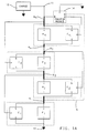
- FIG. 1 is illustrative of a first preferred embodiment which utilises unidirectional boost topology to carry out the present invention.
- a plurality (n) of modules having substantially equivalent terminal voltage ratings, each individually designated M, are further identified by a numerical subscript indicating their series positional relationship in an aggregate multi-module pack.
- the pack comprises at least the illustrated series coupled modules M1 through M n between aggregate pack ground terminal 10 and aggregate pack voltage terminal 11.
- the module coupled directly to aggregate pack ground 10 is identified with the subscript "1" as M1
- the module coupled directly to aggregate pack voltage terminal 11 is identified with the subscript "n" as M n .
- Relative positions of modules when discussed hereafter will be identified with the subscript "x" and numerical progressions therefrom (i.e. M1, M2 ... M x-1 , M x , M x+1 ... M n-1 , M n ).
- Each module M x has a positive and negative terminal, marked (+) and (-) respectively, in accordance with battery terminal convention and a respective module voltage thereacross (VM x ).
- Pack nodes N1 through N n are called out with the same subscript scheme used to identify the modules, each pack node N x being associated with the positive terminal of module M x . Nodes are exaggerated for clarity as heavy dark lines in the illustrations.
- Each module M x therefore has associated therewith a pack node voltage (VN x ) which is defined as the voltage at the respective pack node (N x ) associated with the positive terminal of the corresponding module (M x ) with respect to the aggregate pack ground.
- the aggregate pack voltage is defined as the voltage between aggregate pack voltage terminal 11 and aggregate pack ground 10 and may hereafter be referred to as VP.
- Charge source 12 is shown coupled between aggregate pack voltage terminal 11 and aggregate pack ground 10 for supplying DC charge current to the pack. Specific details of charge source 12 are not discussed herein, it being sufficient to note that the charge source need only provide a DC charge current. It is preferable, of course, that charge source 12 is appropriately either voltage or current controlled to prevent overcharging of the entire pack. Indeed, as part of an overall charging system it is desirable that charge source 12 is controlled to maximise charge efficiency, maximise pack and module life and minimise charge time.
- each module has associated therewith a corresponding converter means, preferably autonomously self-controlled.
- Each of the converter means is individually designated with an upper case C and further identified by a subscript identical to the subscript of the module to which it corresponds for purposes of this description.
- Each converter means is interactively coupled with a pair of modules but is demonstratively grouped with one of the pair herein for reasons which will be more fully developed.
- Each illustrated dashed-line box enclosing a module and corresponding converter means comprises an integral three lead unit.
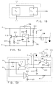
- Figure 1B illustrates one such unit standing alone with the three leads being identified as (+), (-) and EQ.
- the (+) lead is equivalent to a conventional module positive terminal
- the (-) lead is equivalent to a conventional module negative terminal.
- the EQ lead is a charge pump lead which redistributes charge current from a pack node N x associated with a module M x to the adjacent module pack node N x+1 associated with the module M x+1 having the next higher pack node voltage.
- any given converter means senses inequality of respective voltages of a pair of modules.
- the pair of modules comprises two series adjacent modules although any two modules in a pack may comprise a pair provided appropriate isolation circuitry is provided.
- An inequality wherein the module (M x ) with the lesser pack node voltage has a module voltage which exceeds the module voltage of the module (M x+1 ) having the greater pack node voltage causes controlled charge removal from the pack node N x associated with M x and redistribution of the removed charge to the pack node N x+1 associated with M x+1 .
- module M x associated with node N x subject to controlled charge removal may be referred to as the source module
- module M x+1 associated with node N x+1 subject to controlled charge infusion may be referred to as the destination module. Since each of the converter means is of the same boost topology, any redistribution of charge is caused to occur in one direction along the string of modules -- in other words charge is pumped up the string.
- Module M1 is the initial module relative the direction of charge redistribution and module M n is the terminal module relative the direction of charge redistribution.
- the converter means comprises switched mode converter circuitry thereby utilising minimal resistive elements while relying on near lossless energy storing reactive elements for charge redistribution. All of this translates into a very efficient equalisation apparatus which redistributes substantially all diverted charge within the system thereby dissipating minimal energy out of the system.
- a preferred switched mode converter means is described at a later point in conjunction with Figure 4.
- terminal module M n is illustrated having converter means C n associated therewith. This is a preferred arrangement for the terminal module in the direction of charge redistribution, although not a necessity for carrying out the invention. Without converter means C n , module M n may become overcharged since no means would exist for removing charge from pack node N n . With the inclusion of converter means C n in the preferred arrangement, it is necessary to establish another reference voltage in addition to that of module voltage VM n for its operation. A reference voltage that simulates that of a module is provided by phantom module 14. Additionally, a destination for any charge current removed from pack node N n is also needed, which phantom module 14 also provides.
- Phantom module 14 may present a controlled voltage to converter means C n in accordance with a calibrated voltage or alternatively may present a controlled voltage in accordance with the average module voltage "VM avg ".
- the latter referenced voltage scheme is utilised and the voltage presented to converter means C n is substantially the aggregate pack voltage divided by the number of modules VP/n which is equivalent to the average module voltage VM avg .
- Phantom module 14 is shown coupled to aggregate pack voltage VP (terminal 11) at phantom module terminal B, pack ground (terminal 10) at phantom module terminal C, and converter means C n terminal a at phantom module terminal A.
- any charge pumped up to terminal A of phantom module 14 is shunted therethrough to terminal B, the energy associated therewith being dissipated as heat.
- phantom module 14 can be configured such that the charge current pumped up thereto from pack node N n is redistributed within the system to the initial module M1 at pack node N1 as shown by dotted line 16 coupling phantom module 14 terminal D to pack node N1.
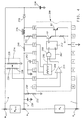
- FIG. 4 an exemplary boost converter topology circuit is illustrated for carrying out the present invention.
- the terminal designations of lower case a,b and c correspond to the same designations of the converters illustrated in the block diagram of Figure 1. While the circuitry illustrated could be fabricated using discrete components, prefabricated monolithic semiconductor switching regulators available in convenient DIP pin packages are the preferred foundation for the embodiment described herein. Shown in Figure 4 is one such 16 pin package, ⁇ A78S40, available commercially from Motorola, utilised in the present embodiment and hereinafter referred to as IC 200. An arbitrary pair of adjacent modules, M x and M x+1 , from a pack are also illustrated and labelled as are appropriate pack nodes, N x-1 , N x and N x+1 .
- FIG. 4 shows pins 3 and 9-16 only are utilised.
- Power for IC 200 is provided at pin 13 from terminal b which is also coupled to the common node N x between two adjacent modules as illustrated in Figure 1.
- IC ground reference for IC 200 is provided at pin 11 from terminal c which is also coupled to the negative terminal (node N x-1 ) of the module having the lesser pack node voltage at its positive terminal relative to the aggregate pack ground as illustrated in Figure 1.
- Each of the plurality of IC ground references is therefore relative to the negative terminal of module M x and should not be confused with the aggregate pack ground.
- External timing capacitor 202 is coupled between the IC ground reference and pin 12 to control the output period and duty cycle of free running oscillator 204. Timing capacitor is charged and discharged in accordance with the circuitry of oscillator 204 to yield an approximate output duty cycle ratio of 6:1 which may be reduced to provide over-current protection as discussed later.
- the oscillator output on line 206 is either a logical "1" or logical "0" input into two input AND gate 208.
- the other input to AND gate 208 is the output of comparator 210 on line 212.
- Comparator 210 has at its inverting input a voltage signal substantially representative of the midpoint voltage of the total voltage across series modules M x and M x+1 .
- the inverting input is coupled to the voltage signal through pin 10 which is itself coupled to voltage divider circuit 214 which establishes the midpoint voltage between terminals a and c.
- the non-inverting input of comparator 210 similarly is coupled to a voltage signal substantially representative of the voltage of the actual voltage at node N x via terminal b and c and resistors 230, 232. If the voltage of module M x is lower than the voltage of module M x+1 then the actual node voltage at N x relative node N x-1 will be lower or more negative than the midpoint voltage across the pair of adjacent modules.
- Comparator 210 is operative to output a logical "1" where the module voltage of M x+1 is less than the module voltage of M x , and a logical "0" where the voltage of M x+1 is greater than the voltage of M x .
- a logical "1" at the output of comparator 210 indicates an inequality as between the two module voltages to which the unidirectional boost topology of the present embodiment is designed to address.
- the logical output of comparator 210 is gated with the logical output of oscillator 204 at AND gate 208. When both logical inputs to AND gate 208 are high, the output of the gate is likewise high and in turn sets the output "Q" of SR latch 212 high via set input "S" thereof.
- Reset input "R" of the latch receives an inverted oscillator output signal via line 206' and as a result, SR latch 212 once set high at output Q will remain set high for so long as the output of oscillator 204 remains high regardless of the logical level of comparator 210. Similarly, once reset low at output Q, SR latch 212 will remain reset at least for so long as comparator 210 output is logical "0". Output Q therefore essentially follows the logical state of oscillator 204 for so long as equalisation is required as indicated by a high output from comparator 210.
- the output Q from SR latch when set is a logical "1" which in turn will force transistors Q1 and Q2 into saturation.
- Diode 216 is thereby reverse biased and current begins to flow out of node N x through over-current resistor 218, inductor 220, transistor Q2 to node N x-1 , thereby energising inductor 220 from module M x .
- transistors Q1 and Q2 are biased non-conductive resulting in a collapse of the magnetic field through inductor 220 and reversal of voltage thereacross.
- Inductor 220 thereby provides current into node N x+1 through diode 216 for charge equalising module M x+1 with module M x .
- Filter capacitor 234 provides output ripple reduction. This cycle of charge redistribution out of node N x and into node N x+1 continues in accordance with the period of oscillator 204 for so long as module M x+1 voltage is less than module M x voltage as indicated by the previously described logical "1" at the output of comparator 210.
- Over-current resistor 218 which, as previously mentioned, passes current contributing to the energization of inductor 220.
- the voltage drop across over-current resistor 218 is monitored at pin 14 which is coupled to overcurrent circuitry of oscillator 204.
- the voltage drop across over-current resistor increases and if it reaches a critical value as predetermined by the overcurrent circuitry of oscillator 204 causes the sourcing of additional charge current to timing capacitor 202 thereby attenuating the oscillator duty cycle for the current period and limiting further sourcing of current through inductor 220.
- Collector resistor 222 is chosen to ensure operation of transistor Q1 in saturation.
- Resistor R1 is nominally 170 ohms as provided internal IC 200. Further details on operation of IC 200 and considerations for external component values may be found in the manufacturers data sheets. The following table lists exemplary external component values for a preferred operative boost converter means used in conjunction with a pair of conventional 12 volt automotive lead acid modules. It should be understood that it may be desirable to alter component values consistent with the objectives and ordinary skill of the designer without deviating from the scope of the invention.
- FIG. 5A a first circuit for a phantom module for use in a unidirectional boost converter topology charge equalisation system as illustrated in Figure 1 is shown.
- This particular phantom module is effective to present a controlled voltage to the converter means C n associated with the terminal module M n substantially equivalent to the aggregate pack voltage VP divided by the number of modules n.
- Charge current redistributed from node N n corresponding to the terminal module M n is shunted and the energy associated therewith is dissipated as heat in order to maintain charge equalisation of the modules.
- terminal module M n is the source module and the phantom module simulates a destination module providing both a simulated module voltage and a charge destination.
- the circuit of Figure 5A generally designated 300 is based around operational amplifier 301. Power and ground are supplied thereto via terminals A and B respectively. As illustrated in Figure 1A, phantom module terminal A is coupled to converter means C n terminal a; phantom module terminal B is coupled to node N n and thereby to converter means C n terminal b; and, phantom module terminal C is coupled to pack ground. Power is coupled through resistor 302 and filter capacitor 303 is coupled between terminal B and resistor 302. Matched value resistors 304 and 305 divide the voltage across terminals A and B and couple it to the inverting input of operational amplifier 301. Capacitor 306 is coupled in negative feedback across the output and inverting input of amplifier 301.
- the non-inverting input of amplifier 301 is coupled to terminal A through resistor 307 and to terminal C through resistors 308 and 309.
- the output of amplifier 301 is coupled to the cathode of zener diode 310.
- the anode of zener diode 310 is coupled to terminal B through resistor 311 and to the base of NPN transistor 312.
- Transistor 312 is coupled to terminal A at its collector and to terminal B through resistor 313 at its emitter.
- circuit 5A is basically a shunt voltage regulator. It regulates a voltage V AB across terminal A and B as some fraction of the voltage V AC across terminal A and C.
- the output stage uses zener diode 310 and resistor 311 to allow transistor 312 to cut off even though amplifier 301 may not achieve an output of zero volts.
- Resistor 313 removes some of the power dissipation from transistor 312 thereby allowing a smaller transistor and providing some overcurrent protection.
- Amplifier 301 uses power bypass filtering of resistor 302 and capacitor 303. Negative feedback capacitor 306 is used to slow the response down thereby stabilising circuit operation.
- the voltage across terminals A and B is regulated when the voltage division provided by matched resistors 304 and 305 at the inverting input equals the voltage division provided by the resistive network 307, 308 and 309 across terminal A and C.
- Values for resistors 307, 308 and 309 are listed below assuming an exemplary pack having five modules.
- Resistor 308 is, as illustrated, a variable resistor used to trim the or fine tune the network.
- FIG. 5B a second circuit for a phantom module for use in a unidirectional boost converter topology charge equalisation system as illustrated in Figure 1A is shown.
- This embodiment of a phantom module closes the loop on the string of modules by (a) presenting module voltage VM1 to converter C n for comparison to the module voltage VM n , and (b) pumping current into node N1 when VM1 ⁇ VM n , thereby simulating adjacency of the terminal and initial modules.
- Isolation circuitry is necessary to accomplish this type of charge redistribution from one module to another module not immediately adjacent thereto.
- This redistributive phantom module designated 400 in FIG 5B comprises a pair of isolation amplifiers 402 and 404. Terminals A, B, C and D correspond to like designations of the phantom module shown in FIG 1A.
- Isolation amplifier 402 has its non-inverting terminal coupled to node N1 corresponding to the positive terminal of the module M1, and has its inverting terminal coupled to the pack ground, thereby presenting module voltage VM1 thereacross.
- the non-inverting terminal of isolation amplifier 402 is also coupled to the emitter of NPN transistor 406.
- the collector of transistor 406 is coupled to power source 420.
- the base of transistor 406 is coupled to the output of operational amplifier 408.
- the non-inverting terminal of amplifier 408 is coupled to ground and the inverting terminal thereof is coupled to the inverting terminal of isolation amplifier 402 through resistor 410 and to the output of isolation amplifier 404 through resistor 412.
- Resistor 414 is shown coupled between terminal C and aggregate pack ground.
- isolation amplifier 402 is coupled to the base of PNP transistor 416.
- the collector of transistor 416 is coupled to node N n corresponding to the module M n and to the output reference of isolation amplifier 402.
- the emitter of transistor 416 is shown coupled to the non-inverting terminal of isolation amplifier 404 and to one side of resistor 418.
- the other side of resistor 418 is commonly coupled to the inverting terminal of isolation amplifier 404, the feedback of isolation amplifier 402 and terminal A of converter means C n .
- module voltage VM1 between terminals C and D is translated to converter C n between terminals A and B via isolation amplifier 402 which uses PNP transistor 416 and limiting resistor 418 as a shunt voltage regulator.
- This is accomplished by using the feedback connection to the isolation operational amplifier in a manner to effect a voltage follower (i.e. the voltage between A and B follows the voltage between D and C).
- the current removed (or shunted) at terminal A is measured by resistor 418 and coupled to a current source connected to terminal D via isolation amplifier 404.
- the current source has a common 425 which is not that of the pack so it requires a floating power source 420.
- the current source is made with a pass transistor 406, error amplifier 408, current measuring shunt 414 and summing resistors 410, 412. Error amplifier 408 biases pass transistor 406 so that the voltage from current shunt 414 and the output voltage from isolation amplifier 404 are equal and opposite. This results in the current at terminal D being proportional to the command voltage at the output of isolation amplifier 404, which in turn is proportional to the current removed from terminal A. Exemplary component values are listed below. Component Value R 410 10 K ⁇ R 412 10 K ⁇ R 414 1 ⁇ R 418 1 ⁇
- a multi-module pack comprises a plurality (n) of modules M x and associated nodes N x identified by numerical subscripts in the manner previously describing Figure 1A.
- Charge source 22 is shown coupled between aggregate pack voltage terminal 21 and aggregate pack ground 20 for supplying DC charge current to the pack, preferably in a controlled manner as previously described.
- unidirectional buck converter topology is utilised in the present embodiment to remove charge from a pack node N x associated with a module M x and redistribute that charge to a pack node N x-1 corresponding to a module M x-1 at a lower aggregate pack voltage.
- terminal b of a converter means comprises the EQ lead for pumping charge into the pack node between a pair of adjacent modules.
- module M x associated with node N x subject to controlled charge removal may be referred to as the source module
- module M x-1 associated with node N x-1 subject to controlled charge infusion may be referred to as the destination module. Since each of the converter means is of the same buck topology, any redistribution of charge is caused to occur in one direction along the string of modules -- in this embodiment charge is pumped down the string. It can therefore be seen that the charge redistribution is unidirectional with respect to both the pair of modules associated with an individual converter means and the series arrangement of modules.
- Module M n is the initial module relative the direction of charge redistribution and module M1 is the terminal module relative the direction of charge redistribution.
- phantom module 24 in Figure 2 provides means for presenting a reference voltage to converter means C1 which simulates that of a charge equalised module.
- this reference voltage is substantially equal to the average module voltage, for example, the aggregate pack voltage divided by the number of modules.
- phantom module 24 provides a destination for charge current removed from node N1.
- Charge current may be shunted and dissipated as heat out of the system or redistributed to module M n as illustrated by line 26 coupling phantom module to node N n thereby retaining energy within the system. If the charge is redistributed to Node N n , then phantom module must be coupled also to node N n-1 as shown by dashed line 28 in order to provide a comparison between module voltages VM n and VM1. Otherwise, line 28 is not required to shunt the charge and dissipate the corresponding energy as heat.
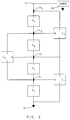
- FIG. 3 Another embodiment of the present charge equalisation invention is illustrated in block diagram Figure 3.
- This figure features a multi-module pack comprised of four modules M1 through M4 to simplify the illustration; however, as with the other embodiments, any number of modules may be employed. Modules and associated nodes are therefore identified by definite numerical subscripts.
- Charge source 32 is shown coupled between aggregate pack voltage terminal 31 and aggregate pack ground 30 for supplying DC charge current to the pack, preferably in a controlled manner as previously described.
- This embodiment in contrast to those of previous description, utilises bidirectional boost/buck topology converters for carrying out charge redistribution from either module in a pair of modules to the other module in the pair. Therefore, each module is both a source and destination module with respect to a commonly coupled converter means.
- An advantage of the bidirectional arrangement is that the number of converters required is one less than either of the two preferred unidirectional arrangements. Additionally, a phantom module is wholly superfluous since all converter means are capable of both removing and contributing charge to any pack node.
- bidirectional converter means tend to be more complicated from a hardware and control standpoint, and further do not have the grouping or packaging advantages of either of the unidirectional arrangements.
Landscapes
- Engineering & Computer Science (AREA)
- Power Engineering (AREA)
- Dc-Dc Converters (AREA)
- Charge And Discharge Circuits For Batteries Or The Like (AREA)
Abstract
Description
- The present invention relates to a module charge equalisation apparatus and method for rechargeable electrochemical batteries.
- Motor vehicles driven by electric motors typically require voltages of significantly greater magnitude than those commonly utilised in conventional internal combustion engine driven motor vehicles for powering accessories. A battery pack made up of at least one series arrangement -- and potentially multiple parallel connected series arrangements -- of individual modules is one common way for achieving a high voltage in a manageable form. Physical characteristics from one module to another are never identical even when modules are produced under the tightest control. This becomes an extremely important consideration in a series arrangement of modules wherein the discharge and charge current is identical through each module. During discharge or re-charge cycling of a series battery pack, one or another of the individual modules reaches -- prior to the remaining modules reaching -- certain physical discharge or re-charge limitations after which damage may occur.
- For example, in conventional lead acid aqueous electrolyte batteries, discharge beyond a certain point may lead to reversal of the electrodes and permanent damage to the module. Re-charge beyond a certain point may lead to gassing of the electrolyte thereby reducing the useful life of the module. Additionally, the module reaching a fully charged state prior to the others will thereby limit the charge of the remaining modules where charging is terminated in response thereto. This "weak link" in the series chain of modules will thereby promote the situation wherein the only fully charged module is the one to first reach that state, resulting in a battery pack which never reaches its full energy capacity.
- It is one object of the present invention to reduce or eliminate the influence that any one module has upon the remaining modules during re-charge of a series arrangement of individual modules.
- To this end, a module charge equalisation apparatus and method in accordance with the present invention is characterised by the features specified in
claims - The present invention preferably equalises the charge to all modules during re-charge such that each module reaches full capacity without detrimental overcharge to any module; and preferably accomplishes the foregoing objectives without microprocessor or other centralised control.
- Therefore, in accordance with one aspect of the present invention, a charge equalisation apparatus is provided utilising a plurality of switched mode power converter means, each effective between a pair of modules for equalising the voltage therebetween. Each power converter is effective to divert charge from the one of the pair of modules having a higher voltage to the other of the pair having the lower voltage.
- According to another aspect of the invention, each of the converter means is effective to divert charge either bidirectionally or unidirectionally between the pair of modules.
- The present invention will now be described, by way of example, with reference to the accompanying drawings, in which:-
- Figure 1A is a block diagram illustrating a distributed charge equalisation apparatus utilising unidirectional boost converter topology in accordance with an embodiment of the present invention;
- Figure 1B illustrates a preferred unitary grouping of a unidirectional boost converter with a module in accordance with an embodiment of the present invention;
- Figure 2 is a block diagram illustrating a distributed charge equalisation apparatus utilising unidirectional buck converter topology in accordance with an embodiment of the present invention;
- Figure 3 is a block diagram illustrating a charge equalisation apparatus utilising bidirectional boost/buck converter topology in accordance with an embodiment of the present invention;
- Figure 4 is a schematic diagram of a preferred unidirectional boost converter as applied to a distributed charge equalisation apparatus illustrated in Figure 1A;
- Figure 5A is a schematic of one system phantom module for charge shunting as illustrated in Figure 1; and
- Figure 5B is a schematic of an alternate system phantom module for charge internalising as illustrated in Figure 1.
- Figure 1 is illustrative of a first preferred embodiment which utilises unidirectional boost topology to carry out the present invention. A plurality (n) of modules having substantially equivalent terminal voltage ratings, each individually designated M, are further identified by a numerical subscript indicating their series positional relationship in an aggregate multi-module pack. The pack comprises at least the illustrated series coupled modules M₁ through Mn between aggregate
pack ground terminal 10 and aggregatepack voltage terminal 11. The module coupled directly toaggregate pack ground 10 is identified with the subscript "1" as M₁, and the module coupled directly to aggregatepack voltage terminal 11 is identified with the subscript "n" as Mn. Relative positions of modules when discussed hereafter will be identified with the subscript "x" and numerical progressions therefrom (i.e. M₁, M₂ ... Mx-1, Mx, Mx+1 ... Mn-1, Mn). - The aggregate pack ground throughout all figures is identified by a solid schematic ground symbol as illustrated in Figure 1. Each module Mx has a positive and negative terminal, marked (+) and (-) respectively, in accordance with battery terminal convention and a respective module voltage thereacross (VMx). Pack nodes N₁ through Nn are called out with the same subscript scheme used to identify the modules, each pack node Nx being associated with the positive terminal of module Mx. Nodes are exaggerated for clarity as heavy dark lines in the illustrations. Each module Mx therefore has associated therewith a pack node voltage (VNx) which is defined as the voltage at the respective pack node (Nx) associated with the positive terminal of the corresponding module (Mx) with respect to the aggregate pack ground. The aggregate pack voltage is defined as the voltage between aggregate
pack voltage terminal 11 andaggregate pack ground 10 and may hereafter be referred to as VP. -
Charge source 12 is shown coupled between aggregatepack voltage terminal 11 andaggregate pack ground 10 for supplying DC charge current to the pack. Specific details ofcharge source 12 are not discussed herein, it being sufficient to note that the charge source need only provide a DC charge current. It is preferable, of course, thatcharge source 12 is appropriately either voltage or current controlled to prevent overcharging of the entire pack. Indeed, as part of an overall charging system it is desirable thatcharge source 12 is controlled to maximise charge efficiency, maximise pack and module life and minimise charge time. - In the present exemplary unidirectional boost topology embodiment of Figure 1, each module has associated therewith a corresponding converter means, preferably autonomously self-controlled. Each of the converter means is individually designated with an upper case C and further identified by a subscript identical to the subscript of the module to which it corresponds for purposes of this description. Each converter means is interactively coupled with a pair of modules but is demonstratively grouped with one of the pair herein for reasons which will be more fully developed. Each illustrated dashed-line box enclosing a module and corresponding converter means comprises an integral three lead unit. Figure 1B illustrates one such unit standing alone with the three leads being identified as (+), (-) and EQ. The (+) lead is equivalent to a conventional module positive terminal, and the (-) lead is equivalent to a conventional module negative terminal. The EQ lead is a charge pump lead which redistributes charge current from a pack node Nx associated with a module Mx to the adjacent module pack node Nx+1 associated with the module Mx+1 having the next higher pack node voltage.
- It is noted that with the described grouping of a module and a converter means charge equalisation is accomplished without the necessity of a cumbersome common charge bus and more complicated converter topologies. Similarly, independent operation of each converter means distributes equalisation control thereby alleviating the necessity of centralised control; although centralised control where desirable may be implemented but is not discussed herein as it is beyond the scope of the present invention. Distributed equalisation allows a virtually unlimited number of series modules to be integrated into a desired pack. As can be seen from Figure 1A, a relatively simple and substantially repetitive coupling configuration allows for such desirable attributes. The grouping of a module together with a converter means into a stand alone unit as shown in Figure 1B and earlier described with reference thereto affords the designer a great deal of system flexibility and simplification.
- In operation, any given converter means senses inequality of respective voltages of a pair of modules. In the present unidirectional embodiment, the pair of modules comprises two series adjacent modules although any two modules in a pack may comprise a pair provided appropriate isolation circuitry is provided. An inequality wherein the module (Mx) with the lesser pack node voltage has a module voltage which exceeds the module voltage of the module (Mx+1) having the greater pack node voltage causes controlled charge removal from the pack node Nx associated with Mx and redistribution of the removed charge to the pack node Nx+1 associated with Mx+1. However, an inequality wherein the module (Mx) with the lesser pack node voltage has a module voltage which is less than the module voltage of the module (Mx+1) having the greater pack node voltage does not cause any charge redistribution. With respect to any pair of modules corresponding to a converter means, module Mx associated with node Nx subject to controlled charge removal may be referred to as the source module, and module Mx+1 associated with node Nx+1 subject to controlled charge infusion may be referred to as the destination module. Since each of the converter means is of the same boost topology, any redistribution of charge is caused to occur in one direction along the string of modules -- in other words charge is pumped up the string. It can therefore be seen that the charge redistribution is unidirectional with respect to both the pair of modules associated with an individual converter means and the series arrangement of modules. Module M₁ is the initial module relative the direction of charge redistribution and module Mn is the terminal module relative the direction of charge redistribution.
- A major advantage to be appreciated is that charge redistribution does not merely shunt current around a module and thereby does not suffer from high energy losses through heat dissipation associated with such techniques. The converter means comprises switched mode converter circuitry thereby utilising minimal resistive elements while relying on near lossless energy storing reactive elements for charge redistribution. All of this translates into a very efficient equalisation apparatus which redistributes substantially all diverted charge within the system thereby dissipating minimal energy out of the system. A preferred switched mode converter means is described at a later point in conjunction with Figure 4.
- Still with reference to Figure 1, terminal module Mn is illustrated having converter means Cn associated therewith. This is a preferred arrangement for the terminal module in the direction of charge redistribution, although not a necessity for carrying out the invention. Without converter means Cn, module Mn may become overcharged since no means would exist for removing charge from pack node Nn. With the inclusion of converter means Cn in the preferred arrangement, it is necessary to establish another reference voltage in addition to that of module voltage VMn for its operation. A reference voltage that simulates that of a module is provided by
phantom module 14. Additionally, a destination for any charge current removed from pack node Nn is also needed, whichphantom module 14 also provides.Phantom module 14 may present a controlled voltage to converter means Cn in accordance with a calibrated voltage or alternatively may present a controlled voltage in accordance with the average module voltage "VMavg". Preferably, the latter referenced voltage scheme is utilised and the voltage presented to converter means Cn is substantially the aggregate pack voltage divided by the number of modules VP/n which is equivalent to the average module voltage VMavg. -
Phantom module 14 is shown coupled to aggregate pack voltage VP (terminal 11) at phantom module terminal B, pack ground (terminal 10) at phantom module terminal C, and converter means Cn terminal a at phantom module terminal A. In operation, any charge pumped up to terminal A ofphantom module 14 is shunted therethrough to terminal B, the energy associated therewith being dissipated as heat. Alternatively,phantom module 14 can be configured such that the charge current pumped up thereto from pack node Nn is redistributed within the system to the initial module M₁ at pack node N₁ as shown by dottedline 16coupling phantom module 14 terminal D to pack node N₁. These two alternative embodiments ofphantom module 14 will be exemplified with respect to specific circuitry as shown in Figures 5A and 5B. - Referring now to Figure 4, an exemplary boost converter topology circuit is illustrated for carrying out the present invention. The terminal designations of lower case a,b and c correspond to the same designations of the converters illustrated in the block diagram of Figure 1. While the circuitry illustrated could be fabricated using discrete components, prefabricated monolithic semiconductor switching regulators available in convenient DIP pin packages are the preferred foundation for the embodiment described herein. Shown in Figure 4 is one such 16 pin package, µA78S40, available commercially from Motorola, utilised in the present embodiment and hereinafter referred to as
IC 200. An arbitrary pair of adjacent modules, Mx and Mx+1, from a pack are also illustrated and labelled as are appropriate pack nodes, Nx-1, Nx and Nx+1. When the module voltage VMx+1 coupled between terminals a and b exceeds the module voltage VMx coupled between terminal b and c, no charge transfer occurs from the pack node Nx to the pack node Nx+1. However, where the module voltage VMx coupled between terminals b and c exceeds the module voltage VMx+1 coupled between terminals a and b, charge transfer is caused to occur from the pack node Nx to the pack node Nx+1. - The preferred configuration of Figure 4 shows
pins 3 and 9-16 only are utilised. Power forIC 200 is provided atpin 13 from terminal b which is also coupled to the common node Nx between two adjacent modules as illustrated in Figure 1. IC ground reference forIC 200 is provided atpin 11 from terminal c which is also coupled to the negative terminal (node Nx-1) of the module having the lesser pack node voltage at its positive terminal relative to the aggregate pack ground as illustrated in Figure 1. Each of the plurality of IC ground references is therefore relative to the negative terminal of module Mx and should not be confused with the aggregate pack ground. -
External timing capacitor 202 is coupled between the IC ground reference andpin 12 to control the output period and duty cycle offree running oscillator 204. Timing capacitor is charged and discharged in accordance with the circuitry ofoscillator 204 to yield an approximate output duty cycle ratio of 6:1 which may be reduced to provide over-current protection as discussed later. The oscillator output online 206 is either a logical "1" or logical "0" input into two input ANDgate 208. The other input to ANDgate 208 is the output ofcomparator 210 online 212.Comparator 210 has at its inverting input a voltage signal substantially representative of the midpoint voltage of the total voltage across series modules Mx and Mx+1. The inverting input is coupled to the voltage signal throughpin 10 which is itself coupled tovoltage divider circuit 214 which establishes the midpoint voltage between terminals a and c. The non-inverting input ofcomparator 210 similarly is coupled to a voltage signal substantially representative of the voltage of the actual voltage at node Nx via terminal b and c andresistors -
Comparator 210 is operative to output a logical "1" where the module voltage of Mx+1 is less than the module voltage of Mx, and a logical "0" where the voltage of Mx+1 is greater than the voltage of Mx. A logical "1" at the output ofcomparator 210 indicates an inequality as between the two module voltages to which the unidirectional boost topology of the present embodiment is designed to address. The logical output ofcomparator 210 is gated with the logical output ofoscillator 204 at ANDgate 208. When both logical inputs to ANDgate 208 are high, the output of the gate is likewise high and in turn sets the output "Q" ofSR latch 212 high via set input "S" thereof. Reset input "R" of the latch receives an inverted oscillator output signal via line 206' and as a result,SR latch 212 once set high at output Q will remain set high for so long as the output ofoscillator 204 remains high regardless of the logical level ofcomparator 210. Similarly, once reset low at output Q,SR latch 212 will remain reset at least for so long ascomparator 210 output is logical "0". Output Q therefore essentially follows the logical state ofoscillator 204 for so long as equalisation is required as indicated by a high output fromcomparator 210. - The output Q from SR latch when set is a logical "1" which in turn will force transistors Q1 and Q2 into saturation.
Diode 216 is thereby reverse biased and current begins to flow out of node Nx throughover-current resistor 218,inductor 220, transistor Q2 to node Nx-1, thereby energisinginductor 220 from module Mx. When the output Q from SR latch goes to a logical "0", transistors Q1 and Q2 are biased non-conductive resulting in a collapse of the magnetic field throughinductor 220 and reversal of voltage thereacross.Inductor 220 thereby provides current into node Nx+1 throughdiode 216 for charge equalising module Mx+1 with module Mx. Filter capacitor 234 provides output ripple reduction. This cycle of charge redistribution out of node Nx and into node Nx+1 continues in accordance with the period ofoscillator 204 for so long as module Mx+1 voltage is less than module Mx voltage as indicated by the previously described logical "1" at the output ofcomparator 210. - Current limiting is one feature of the present embodiment provided through use of an appropriate
over-current resistor 218 which, as previously mentioned, passes current contributing to the energization ofinductor 220. The voltage drop acrossover-current resistor 218 is monitored atpin 14 which is coupled to overcurrent circuitry ofoscillator 204. As the current throughinductor 220 ramps up, the voltage drop across over-current resistor increases and if it reaches a critical value as predetermined by the overcurrent circuitry ofoscillator 204 causes the sourcing of additional charge current to timingcapacitor 202 thereby attenuating the oscillator duty cycle for the current period and limiting further sourcing of current throughinductor 220.Collector resistor 222 is chosen to ensure operation of transistor Q1 in saturation. Resistor R1 is nominally 170 ohms as providedinternal IC 200. Further details on operation ofIC 200 and considerations for external component values may be found in the manufacturers data sheets. The following table lists exemplary external component values for a preferred operative boost converter means used in conjunction with a pair of conventional 12 volt automotive lead acid modules. It should be understood that it may be desirable to alter component values consistent with the objectives and ordinary skill of the designer without deviating from the scope of the invention.Component Value R 230 10 KΩ R 232 10 KΩ R 224 10 KΩ R 226 3.3 KΩ R 228 100 KΩ R 218 0.22 Ω R 222 36 Ω C 236 470 µF C 234 470 µF C 202 680 pF L 220 180 µH - Referring now to Figure 5A, a first circuit for a phantom module for use in a unidirectional boost converter topology charge equalisation system as illustrated in Figure 1 is shown. This particular phantom module is effective to present a controlled voltage to the converter means Cn associated with the terminal module Mn substantially equivalent to the aggregate pack voltage VP divided by the number of modules n. Charge current redistributed from node Nn corresponding to the terminal module Mn is shunted and the energy associated therewith is dissipated as heat in order to maintain charge equalisation of the modules. In this embodiment, terminal module Mn is the source module and the phantom module simulates a destination module providing both a simulated module voltage and a charge destination.
- The circuit of Figure 5A generally designated 300 is based around
operational amplifier 301. Power and ground are supplied thereto via terminals A and B respectively. As illustrated in Figure 1A, phantom module terminal A is coupled to converter means Cn terminal a; phantom module terminal B is coupled to node Nn and thereby to converter means Cn terminal b; and, phantom module terminal C is coupled to pack ground. Power is coupled throughresistor 302 andfilter capacitor 303 is coupled between terminal B andresistor 302. Matchedvalue resistors operational amplifier 301.Capacitor 306 is coupled in negative feedback across the output and inverting input ofamplifier 301. The non-inverting input ofamplifier 301 is coupled to terminal A throughresistor 307 and to terminal C throughresistors amplifier 301 is coupled to the cathode ofzener diode 310. The anode ofzener diode 310 is coupled to terminal B throughresistor 311 and to the base ofNPN transistor 312.Transistor 312 is coupled to terminal A at its collector and to terminal B throughresistor 313 at its emitter. - In operation, circuit 5A is basically a shunt voltage regulator. It regulates a voltage VAB across terminal A and B as some fraction of the voltage VAC across terminal A and C. The output stage uses
zener diode 310 andresistor 311 to allowtransistor 312 to cut off even thoughamplifier 301 may not achieve an output of zero volts.Resistor 313 removes some of the power dissipation fromtransistor 312 thereby allowing a smaller transistor and providing some overcurrent protection.Amplifier 301 uses power bypass filtering ofresistor 302 andcapacitor 303.Negative feedback capacitor 306 is used to slow the response down thereby stabilising circuit operation. The voltage across terminals A and B is regulated when the voltage division provided by matchedresistors resistive network 
resistive network

resistors Resistor 308 is, as illustrated, a variable resistor used to trim the or fine tune the network.Component Value R 302 10 Ω R 304100 KΩ R 305 100 KΩ R 307 100 KΩ R 308 200 KΩ R 309 4.75 KΩ R 311 10 KΩ R 313 10 Ω C 303 0.1 µF C 306 0.1 µF - Referring to Figure 5B, a second circuit for a phantom module for use in a unidirectional boost converter topology charge equalisation system as illustrated in Figure 1A is shown. This embodiment of a phantom module, however, closes the loop on the string of modules by (a) presenting module voltage VM₁ to converter Cn for comparison to the module voltage VMn, and (b) pumping current into node N₁ when VM₁<VMn, thereby simulating adjacency of the terminal and initial modules. Isolation circuitry is necessary to accomplish this type of charge redistribution from one module to another module not immediately adjacent thereto.
- This redistributive phantom module designated 400 in FIG 5B comprises a pair of
isolation amplifiers Isolation amplifier 402 has its non-inverting terminal coupled to node N₁ corresponding to the positive terminal of the module M₁, and has its inverting terminal coupled to the pack ground, thereby presenting module voltage VM₁ thereacross. The non-inverting terminal ofisolation amplifier 402 is also coupled to the emitter ofNPN transistor 406. The collector oftransistor 406 is coupled topower source 420. The base oftransistor 406 is coupled to the output ofoperational amplifier 408. The non-inverting terminal ofamplifier 408 is coupled to ground and the inverting terminal thereof is coupled to the inverting terminal ofisolation amplifier 402 throughresistor 410 and to the output ofisolation amplifier 404 throughresistor 412.Resistor 414 is shown coupled between terminal C and aggregate pack ground. - The output of
isolation amplifier 402 is coupled to the base ofPNP transistor 416. The collector oftransistor 416 is coupled to node Nn corresponding to the module Mn and to the output reference ofisolation amplifier 402. The emitter oftransistor 416 is shown coupled to the non-inverting terminal ofisolation amplifier 404 and to one side ofresistor 418. The other side ofresistor 418 is commonly coupled to the inverting terminal ofisolation amplifier 404, the feedback ofisolation amplifier 402 and terminal A of converter means Cn. - In operation, module voltage VM₁ between terminals C and D is translated to converter Cn between terminals A and B via
isolation amplifier 402 which usesPNP transistor 416 and limitingresistor 418 as a shunt voltage regulator. This is accomplished by using the feedback connection to the isolation operational amplifier in a manner to effect a voltage follower (i.e. the voltage between A and B follows the voltage between D and C). The current removed (or shunted) at terminal A (terminal a of converter Cn) is measured byresistor 418 and coupled to a current source connected to terminal D viaisolation amplifier 404. The current source has a common 425 which is not that of the pack so it requires a floatingpower source 420. The current source is made with apass transistor 406,error amplifier 408, current measuringshunt 414 and summingresistors Error amplifier 408 biases passtransistor 406 so that the voltage fromcurrent shunt 414 and the output voltage fromisolation amplifier 404 are equal and opposite. This results in the current at terminal D being proportional to the command voltage at the output ofisolation amplifier 404, which in turn is proportional to the current removed from terminal A. Exemplary component values are listed below.Component Value R 410 10 KΩ R 412 10 KΩ R 414 1 Ω R 418 1 Ω - Embodiments of alternative unidirectional and bidirectional switched mode converter topologies for carrying forward the present invention are illustrated in block diagrams in Figures 2 and 3 respectively. With reference to Figure 2, a multi-module pack comprises a plurality (n) of modules Mx and associated nodes Nx identified by numerical subscripts in the manner previously describing Figure 1A. Charge
source 22 is shown coupled between aggregatepack voltage terminal 21 andaggregate pack ground 20 for supplying DC charge current to the pack, preferably in a controlled manner as previously described. - In the embodiment illustrated in Figure 2, charge redistribution is caused to occur in a unidirectional fashion substantially similar to that described in conjunction with Figure 1. However, unidirectional buck converter topology is utilised in the present embodiment to remove charge from a pack node Nx associated with a module Mx and redistribute that charge to a pack node Nx-1 corresponding to a module Mx-1 at a lower aggregate pack voltage. In this arrangement as illustrated, terminal b of a converter means comprises the EQ lead for pumping charge into the pack node between a pair of adjacent modules. With respect to any pair of modules corresponding to a converter means, module Mx associated with node Nx subject to controlled charge removal may be referred to as the source module, and module Mx-1 associated with node Nx-1 subject to controlled charge infusion may be referred to as the destination module. Since each of the converter means is of the same buck topology, any redistribution of charge is caused to occur in one direction along the string of modules -- in this embodiment charge is pumped down the string. It can therefore be seen that the charge redistribution is unidirectional with respect to both the pair of modules associated with an individual converter means and the series arrangement of modules. Module Mn is the initial module relative the direction of charge redistribution and module M₁ is the terminal module relative the direction of charge redistribution.
- Like the unidirectional boost topology previously discussed with reference to Figure 1, it is desirable to have a converter means C₁ associated with the terminal module in the direction of charge redistribution, although not absolutely necessary to carry out the invention. Without converter means C₁, module M₁ may become overcharged since no means would exist for removing charge from pack node N₁. Analogous to
phantom module 14 in the Figure 1 illustration of unidirectional boost topology,phantom module 24 in Figure 2 provides means for presenting a reference voltage to converter means C₁ which simulates that of a charge equalised module. Preferably, this reference voltage is substantially equal to the average module voltage, for example, the aggregate pack voltage divided by the number of modules. Also,phantom module 24 provides a destination for charge current removed from node N₁. Charge current may be shunted and dissipated as heat out of the system or redistributed to module Mn as illustrated byline 26 coupling phantom module to node Nn thereby retaining energy within the system. If the charge is redistributed to Node Nn, then phantom module must be coupled also to node Nn-1 as shown by dashedline 28 in order to provide a comparison between module voltages VMn and VM₁. Otherwise,line 28 is not required to shunt the charge and dissipate the corresponding energy as heat. - Another embodiment of the present charge equalisation invention is illustrated in block diagram Figure 3. This figure features a multi-module pack comprised of four modules M₁ through M₄ to simplify the illustration; however, as with the other embodiments, any number of modules may be employed. Modules and associated nodes are therefore identified by definite numerical subscripts. Charge
source 32 is shown coupled between aggregatepack voltage terminal 31 andaggregate pack ground 30 for supplying DC charge current to the pack, preferably in a controlled manner as previously described. - This embodiment, in contrast to those of previous description, utilises bidirectional boost/buck topology converters for carrying out charge redistribution from either module in a pair of modules to the other module in the pair. Therefore, each module is both a source and destination module with respect to a commonly coupled converter means. An advantage of the bidirectional arrangement is that the number of converters required is one less than either of the two preferred unidirectional arrangements. Additionally, a phantom module is wholly superfluous since all converter means are capable of both removing and contributing charge to any pack node. However, bidirectional converter means tend to be more complicated from a hardware and control standpoint, and further do not have the grouping or packaging advantages of either of the unidirectional arrangements.
- The disclosures in United States patent application no. 178,170, from which this application claims priority, and in the abstract accompanying this application are incorporated herein by reference.
Claims (14)
- A module charge equalisation apparatus for a rechargeable electrochemical battery system having a series arrangement of electrochemical modules (Mn) to define a battery pack, each module having a positive and negative terminal and a respective module voltage thereacross, the battery pack having an aggregate pack voltage terminal (11) and an aggregate pack ground terminal (10), each module further having a corresponding pack node voltage across its respective positive terminal and the aggregate pack ground terminal, the module charge equalisation apparatus comprising a charging source (12) couplable across the aggregate pack voltage terminal and aggregate pack ground terminal; and a plurality of switched mode power converter means (Cn), each switched mode power converter means being responsive to the respective module voltages of a pair of modules corresponding thereto, and each of the switch mode power converter means being operative in one ofa) a first mode effective to electrically couple the switched mode power converter means to the pair of modules to divert charge from one of the pair of modules to the other of the pair of modules when the module voltage of said one module exceeds the module voltage of said other module, andb) a second mode effective to electrically decouple the switched mode power converter means from the pair of modules.
- A module charge equalisation apparatus as claimed in claim 1, wherein each of the switched mode power converter means is operative in the first mode to divert charge unidirectionally from the positive terminal of a source module of the pair of modules to the positive terminal of a destination module of the pair of modules when the module voltage of the source module exceeds the module voltage of the destination module.
- A module charge equalisation apparatus as claimed in claim 2, further comprising means (14) for generating a simulated module voltage and presenting the simulated module voltage as the destination module to a converter means which has as the source module a terminal module relative the direction of charge redistribution.
- A module charge equalisation apparatus as claimed in claim 3, wherein the means (24) for generating a simulated module voltage comprises charge destination means operative to shunt the charge diverted from the positive terminal of the terminal module.
- A module charge equalisation apparatus as claimed in claim 3, wherein the means for generating a simulated module voltage comprises charge destination means operative to redistribute the charge diverted from the positive terminal of the terminal module to the positive terminal of an initial module relative the direction of charge redistribution.
- A module charge equalisation apparatus as claimed in claim 2, wherein the source module of the pair of modules comprises the one module of pair of modules having a greater pack node voltage than the other module of the pair of modules.
- A module charge equalisation apparatus as claimed in claim 2, wherein the source module of the pair of modules comprises the one module of the pair of modules having a lesser pack node voltage than the other module of the pair of modules.
- A module charge equalisation apparatus as claimed in claim 2, wherein each of the switched mode power converter means comprises boost converter topology.
- A module charge equalisation apparatus as claimed in claim 2, wherein each of the switched mode power converter means comprises buck converter topology.
- A method of module charge equalisation in a rechargeable electrochemical battery system having a series arrangement of electrochemical modules (Mn) to define a battery pack, each module having a positive and negative terminal and a respective module voltage thereacross, the battery pack having an aggregate pack voltage terminal (11) and an aggregate pack ground terminal (10), each module further having a corresponding pack node voltage across its respective positive terminal and the aggregate pack ground terminal, the method comprising the steps of supplying current into the aggregate pack voltage terminal; comparing a pair of module voltages; removing current from the positive terminal of the one of the pair of modules having a greater module voltage; and supplying the removed current to the positive terminal of the other of the pair of modules having a lesser module voltage.
- A method as claimed in claim 10, wherein the steps of removing and supplying current are carried out bidirectionally by boost/buck converter topology.
- A method as claimed in claim 10, wherein the steps of removing and supplying current are carried out unidirectionally by one of (a) boost converter topology, and (b) buck converter topology.
- A method as claimed in claim 12, wherein the steps of comparing, removing and supplying are performed on a pair of adjacent modules.
- A method as claimed in claim 12, wherein a terminal module and an initial module comprise a pair of adjacent modules.
Applications Claiming Priority (2)
| Application Number | Priority Date | Filing Date | Title |
|---|---|---|---|
| US17817094A | 1994-01-06 | 1994-01-06 | |
| US178170 | 1994-01-06 |
Publications (3)
| Publication Number | Publication Date |
|---|---|
| EP0662744A2 true EP0662744A2 (en) | 1995-07-12 |
| EP0662744A3 EP0662744A3 (en) | 1996-01-03 |
| EP0662744B1 EP0662744B1 (en) | 1999-03-24 |
Family
ID=22651487
Family Applications (1)
| Application Number | Title | Priority Date | Filing Date |
|---|---|---|---|
| EP94203571A Expired - Lifetime EP0662744B1 (en) | 1994-01-06 | 1994-12-08 | Module charge equalisation apparatus and method |
Country Status (4)
| Country | Link |
|---|---|
| US (1) | US5592067A (en) |
| EP (1) | EP0662744B1 (en) |
| JP (1) | JPH07212984A (en) |
| DE (1) | DE69417385T2 (en) |
Cited By (11)
| Publication number | Priority date | Publication date | Assignee | Title |
|---|---|---|---|---|
| DE19526836A1 (en) * | 1995-07-22 | 1997-01-23 | Fraunhofer Ges Forschung | Charge balancing device between a plurality of energy stores or converters |
| WO1997016879A1 (en) * | 1995-10-31 | 1997-05-09 | Xicon Battery Electronics Ab | System for equalizing the level of charge in batteries |
| EP0767524A3 (en) * | 1995-10-04 | 1997-07-23 | Motorola Inc | Method and structure for balancing energy sources |
| WO1998009364A1 (en) * | 1996-08-30 | 1998-03-05 | Telefonaktiebolaget Lm Ericsson (Publ) | Method and device for controlling the voltage across individual cells in a battery |
| WO1998053335A3 (en) * | 1997-05-20 | 1999-02-25 | Usko Jokinen | Condition monitoring system for batteries |
| EP0913292A2 (en) | 1997-10-30 | 1999-05-06 | Lockheed Martin Corporation | Method for equalizing the voltage of traction battery modules of a hybrid electric vehicle |
| EP0691725B1 (en) * | 1994-07-04 | 1999-10-06 | Alcatel | Controlling device for an electric storage battery |
| AU749477B2 (en) * | 1997-05-20 | 2002-06-27 | Usko Jokinen | Condition monitoring system for batteries |
| WO2007087662A3 (en) * | 2006-02-02 | 2008-09-12 | Martin Wieger | Method and arrangement for modifying the state of charge (soc) and state of health (soh) of a battery |
| EP1800380A4 (en) * | 2004-06-04 | 2009-06-24 | Maxwell Technologies Inc | Voltage balancing circuit for multi-cell modules |
| WO2010103182A3 (en) * | 2009-03-13 | 2010-12-16 | Oy Finnish Electric Vehicle Technologies Ltd | Charge management of a battery pack |
Families Citing this family (37)
| Publication number | Priority date | Publication date | Assignee | Title |
|---|---|---|---|---|
| DE4427077C1 (en) * | 1994-07-30 | 1996-03-21 | Fraunhofer Ges Forschung | Device for the exchange of charges between a plurality of energy stores or converters connected in pure |
| WO1998007226A1 (en) * | 1996-08-09 | 1998-02-19 | Volkswagen Aktiengesellschaft | Process and device for monitoring and/or controlling charging of a modular battery, particularly in a battery powered vehicle |
| JP3304777B2 (en) * | 1996-08-22 | 2002-07-22 | トヨタ自動車株式会社 | Electric vehicle |
| US5900716A (en) * | 1997-03-03 | 1999-05-04 | Northrop Grumman Corporation | Balanced battery charger |
| US6031355A (en) * | 1997-08-16 | 2000-02-29 | Rich; Joe G. | Circuit utilizing current flowing from a high-potential battery bank to a low-potential battery bank |
| US5821734A (en) * | 1997-08-29 | 1998-10-13 | Compaq Computer Corporation | Converting battery module with resistor programmation of default output voltage |
| US5945807A (en) * | 1997-08-29 | 1999-08-31 | Compaq Computer Corporation | Converting battery module with battery-powered controller |
| US6222341B1 (en) * | 1997-09-17 | 2001-04-24 | Johnson Controls Technology Company | Dual battery charge maintenance system and method |
| US5965996A (en) * | 1997-12-11 | 1999-10-12 | Vectrix Corporation | Electrical scooter having an equalization circuit for charging multiple batteries |
| US6064178A (en) * | 1998-05-07 | 2000-05-16 | Ford Motor Company | Battery charge balancing system having parallel switched energy storage elements |
| US6169334B1 (en) | 1998-10-27 | 2001-01-02 | Capstone Turbine Corporation | Command and control system and method for multiple turbogenerators |
| US6331365B1 (en) | 1998-11-12 | 2001-12-18 | General Electric Company | Traction motor drive system |
| US6172479B1 (en) | 1999-03-04 | 2001-01-09 | Baxter International Inc. | Battery control circuit |
| US6410992B1 (en) | 2000-08-23 | 2002-06-25 | Capstone Turbine Corporation | System and method for dual mode control of a turbogenerator/motor |
| US6285161B1 (en) * | 2000-09-11 | 2001-09-04 | O2 Micro International Limited | Battery cell charging system having voltage threshold and bleeder current generating circuits |
| AU2002224346A1 (en) | 2000-10-04 | 2002-04-15 | Leonardo Technologies, Inc. | Thermoelectric generators |
| US6664757B1 (en) * | 2002-06-20 | 2003-12-16 | Ford Motor Company | Method and assembly for selectively charging a high voltage vehicular battery |
| US7378818B2 (en) * | 2002-11-25 | 2008-05-27 | Tiax Llc | Bidirectional power converter for balancing state of charge among series connected electrical energy storage units |
| WO2004097868A2 (en) * | 2003-04-25 | 2004-11-11 | Maxwell Technologies, Inc. | Charge balancing circuit for double-layer capacitors |
| FR2860352B1 (en) * | 2003-09-29 | 2006-02-24 | Thales Sa | SYSTEM FOR BALANCING AN ENERGY STORAGE DEVICE |
| US20050285564A1 (en) * | 2004-06-25 | 2005-12-29 | Ford Global Technologies, Llc | Automatic charging of a high voltage battery in a hybrid electric vehicle |
| US7928691B2 (en) * | 2004-11-10 | 2011-04-19 | EaglePicher Technologies | Method and system for cell equalization with isolated charging sources |
| US20060097700A1 (en) * | 2004-11-10 | 2006-05-11 | Eaglepicher Technologies, Llc | Method and system for cell equalization with charging sources and shunt regulators |
| US20060097697A1 (en) * | 2004-11-10 | 2006-05-11 | Eaglepicher Technologies, Llc | Method and system for cell equalization with switched charging sources |
| US7450619B2 (en) * | 2005-06-09 | 2008-11-11 | Mindspeed Technologies, Inc. | Laser driver loop control and method |
| JP4546493B2 (en) * | 2007-02-26 | 2010-09-15 | Udトラックス株式会社 | Cell voltage equalization device for capacitor module |
| US8558508B2 (en) * | 2007-06-08 | 2013-10-15 | C & C Power, Inc. | Battery system and management method |
| US8288992B2 (en) * | 2009-01-14 | 2012-10-16 | Indy Power Systems, Llc | Cell management system |
| US20100289453A1 (en) * | 2009-05-15 | 2010-11-18 | Ford Global Technologies, Llc | Vehicle power system |
| CN102823104B (en) * | 2010-02-05 | 2016-05-11 | 法国原子能源和替代能源委员会 | Charge equalization system for batteries |
| US8723482B2 (en) * | 2010-11-04 | 2014-05-13 | Elite Power Solutions Llc | Battery unit balancing system |
| DE102011079253A1 (en) * | 2011-07-15 | 2013-01-17 | Osram Ag | Circuit arrangement for equalizing state of charge of series-connected energy storage device of battery, has energy storage device which is connected parallelly with respect to series circuit of secondary winding of transformer |
| JP2015100213A (en) * | 2013-11-19 | 2015-05-28 | 蔡富生 | Method and apparatus for executing battery cell control with support of virtual battery mechanism |
| US20170166078A1 (en) * | 2015-12-11 | 2017-06-15 | Ford Global Technologies, Llc | Battery charge equalization system |
| US11153819B2 (en) * | 2017-02-06 | 2021-10-19 | Itron Networked Solutions, Inc. | Battery control for safeguarding lower voltage integrated circuits |
| US10749218B2 (en) * | 2017-11-10 | 2020-08-18 | Qualcomm Incorporated | Circuitry for charging a multi-stack battery pack |
| DE102019208042A1 (en) * | 2019-06-03 | 2020-12-03 | Robert Bosch Gmbh | Method for operating an electrical energy store, electrical energy store and device |
Family Cites Families (14)
| Publication number | Priority date | Publication date | Assignee | Title |
|---|---|---|---|---|
| DE432639C (en) * | 1924-05-14 | 1926-08-07 | Ernst Hoffmann | Jumping stilt-like sports equipment that is strapped to the shoe |
| US3623139A (en) * | 1969-11-06 | 1971-11-23 | Gen Electric | Method and apparatus for automatically controlling the fast charging of rechargeable batteries |
| US4079303A (en) * | 1976-07-28 | 1978-03-14 | The United States Of America As Represented By The United States Department Of Energy | Charging system and method for multicell storage batteries |
| US4303877A (en) * | 1978-05-05 | 1981-12-01 | Brown, Boveri & Cie Aktiengesellschaft | Circuit for protecting storage cells |
| US4238721A (en) * | 1979-02-06 | 1980-12-09 | The United States Of America As Represented By The United States Department Of Energy | System and method for charging electrochemical cells in series |
| SE451924B (en) * | 1982-10-12 | 1987-11-02 | Ericsson Telefon Ab L M | REGULATOR FOR REGULATING A CHARGING CURRENT TO A SINGLE CELL IN A BATTERY OF CELLS |
| US4713597A (en) * | 1985-12-04 | 1987-12-15 | Powerplex Technologies, Inc. | Silicon diode looping element for protecting a battery cell |
| US4743830A (en) * | 1987-01-20 | 1988-05-10 | General Motors Corporation | Dual voltage electrical system |
| JPH088116B2 (en) * | 1988-07-01 | 1996-01-29 | トヨタ自動車株式会社 | Complete discharge method for equalization of metal / halogen battery and metal / halogen battery used for the same |
| US5003244A (en) * | 1989-05-09 | 1991-03-26 | Digital Equipment Corporation | Battery charger for charging a plurality of batteries |
| DE3940928C1 (en) * | 1989-12-12 | 1991-07-11 | Fraunhofer-Gesellschaft Zur Foerderung Der Angewandten Forschung Ev, 8000 Muenchen, De | |
| DE3940929C1 (en) * | 1989-12-12 | 1991-05-08 | Fraunhofer-Gesellschaft Zur Foerderung Der Angewandten Forschung Ev, 8000 Muenchen, De | |
| US5063340A (en) * | 1990-10-25 | 1991-11-05 | Motorola, Inc. | Capacitive power supply having charge equalization circuit |
| US5479083A (en) * | 1993-06-21 | 1995-12-26 | Ast Research, Inc. | Non-dissipative battery charger equalizer |
-
1994
- 1994-12-08 DE DE69417385T patent/DE69417385T2/en not_active Expired - Fee Related
- 1994-12-08 EP EP94203571A patent/EP0662744B1/en not_active Expired - Lifetime
-
1995
- 1995-01-06 JP JP7000634A patent/JPH07212984A/en active Pending
- 1995-01-23 US US08/376,631 patent/US5592067A/en not_active Expired - Fee Related
Cited By (16)
| Publication number | Priority date | Publication date | Assignee | Title |
|---|---|---|---|---|
| EP0691725B1 (en) * | 1994-07-04 | 1999-10-06 | Alcatel | Controlling device for an electric storage battery |
| DE19526836A1 (en) * | 1995-07-22 | 1997-01-23 | Fraunhofer Ges Forschung | Charge balancing device between a plurality of energy stores or converters |
| WO1997004513A1 (en) * | 1995-07-22 | 1997-02-06 | Fraunhofer-Gesellschaft zur Förderung der angewandten Forschung e.V. | Device for equalizing the charges in a multiplicity of accumulators or power converters |
| DE19526836C2 (en) * | 1995-07-22 | 1998-07-02 | Fraunhofer Ges Forschung | Charge balancing device between at least two energy stores or converters |
| EP0767524A3 (en) * | 1995-10-04 | 1997-07-23 | Motorola Inc | Method and structure for balancing energy sources |
| WO1997016879A1 (en) * | 1995-10-31 | 1997-05-09 | Xicon Battery Electronics Ab | System for equalizing the level of charge in batteries |
| CN1080017C (en) * | 1995-10-31 | 2002-02-27 | 西肯电池电子学公司 | System for equalizing level of charge in batteries |
| US5945804A (en) * | 1996-08-30 | 1999-08-31 | Telefonaktiebolaget Lm Ericsson | Method and device for controlling the voltage across individual cells in a battery |
| WO1998009364A1 (en) * | 1996-08-30 | 1998-03-05 | Telefonaktiebolaget Lm Ericsson (Publ) | Method and device for controlling the voltage across individual cells in a battery |
| WO1998053335A3 (en) * | 1997-05-20 | 1999-02-25 | Usko Jokinen | Condition monitoring system for batteries |
| AU749477B2 (en) * | 1997-05-20 | 2002-06-27 | Usko Jokinen | Condition monitoring system for batteries |
| EP0913292A2 (en) | 1997-10-30 | 1999-05-06 | Lockheed Martin Corporation | Method for equalizing the voltage of traction battery modules of a hybrid electric vehicle |
| EP0913292A3 (en) * | 1997-10-30 | 1999-12-29 | Lockheed Martin Corporation | Method for equalizing the voltage of traction battery modules of a hybrid electric vehicle |
| EP1800380A4 (en) * | 2004-06-04 | 2009-06-24 | Maxwell Technologies Inc | Voltage balancing circuit for multi-cell modules |
| WO2007087662A3 (en) * | 2006-02-02 | 2008-09-12 | Martin Wieger | Method and arrangement for modifying the state of charge (soc) and state of health (soh) of a battery |
| WO2010103182A3 (en) * | 2009-03-13 | 2010-12-16 | Oy Finnish Electric Vehicle Technologies Ltd | Charge management of a battery pack |
Also Published As
| Publication number | Publication date |
|---|---|
| EP0662744A3 (en) | 1996-01-03 |
| EP0662744B1 (en) | 1999-03-24 |
| DE69417385D1 (en) | 1999-04-29 |
| DE69417385T2 (en) | 1999-07-15 |
| JPH07212984A (en) | 1995-08-11 |
| US5592067A (en) | 1997-01-07 |
Similar Documents
| Publication | Publication Date | Title |
|---|---|---|
| EP0662744B1 (en) | Module charge equalisation apparatus and method | |
| JP3279071B2 (en) | Battery pack charging device | |
| KR101865442B1 (en) | Battery system | |
| US7800346B2 (en) | Device and method for equalizing charges of series-connected energy stores | |
| CN109039136B (en) | Power assembly system based on modularized multi-level converter | |
| Kutkut et al. | Charge equalization for an electric vehicle battery system | |
| US5710504A (en) | Switched capacitor system for automatic battery equalization | |
| US6271646B1 (en) | Battery cell by-pass circuit | |
| Kimball et al. | Increased performance of battery packs by active equalization | |
| AU637328B2 (en) | Battery charger | |
| US7394225B2 (en) | Pseudo constant current multiple cell battery charger configured with a parallel topology | |
| EP0752748B1 (en) | Multiple function battery charger, self-configuring as supply voltage regulator for battery powered apparatuses | |
| EP0914701A1 (en) | Auxiliary battery voltage/temperature compensation for automotive 12 volt system for electric vehicles | |
| US5754384A (en) | Overcurrent protection circuitry for non-isolated battery discharge controller | |
| JP2003513605A (en) | Modular battery charge equalizer and control method | |
| US5642029A (en) | Constant current battery charger with auxiliary output for portable apparatus | |
| JP3629791B2 (en) | Charge control device for battery pack | |
| US20230208151A1 (en) | Battery Unit, Method, and Apparatus for Operating the Battery Unit | |
| EP0545633A1 (en) | Improvements in battery charging | |
| CN211629888U (en) | Charging device | |
| KR102619260B1 (en) | Serial Battery Cell Charging-Discharging Apparatus | |
| KR20240025555A (en) | Bi-directional adaptive terminal voltage (BATV) of the battery pack | |
| JP2995142B2 (en) | Series battery charger | |
| CA1268518A (en) | Power generator | |
| JP3071491B2 (en) | Battery charger |
Legal Events
| Date | Code | Title | Description |
|---|---|---|---|
| PUAI | Public reference made under article 153(3) epc to a published international application that has entered the european phase |
Free format text: ORIGINAL CODE: 0009012 |
|
| AK | Designated contracting states |
Kind code of ref document: A2 Designated state(s): DE FR GB |
|
| PUAL | Search report despatched |
Free format text: ORIGINAL CODE: 0009013 |
|
| AK | Designated contracting states |
Kind code of ref document: A3 Designated state(s): DE FR GB |
|
| 17P | Request for examination filed |
Effective date: 19960703 |
|
| 17Q | First examination report despatched |
Effective date: 19970821 |
|
| GRAG | Despatch of communication of intention to grant |
Free format text: ORIGINAL CODE: EPIDOS AGRA |
|
| GRAG | Despatch of communication of intention to grant |
Free format text: ORIGINAL CODE: EPIDOS AGRA |
|
| GRAH | Despatch of communication of intention to grant a patent |
Free format text: ORIGINAL CODE: EPIDOS IGRA |
|
| GRAH | Despatch of communication of intention to grant a patent |
Free format text: ORIGINAL CODE: EPIDOS IGRA |
|
| GRAA | (expected) grant |
Free format text: ORIGINAL CODE: 0009210 |
|
| AK | Designated contracting states |
Kind code of ref document: B1 Designated state(s): DE FR GB |
|
| REF | Corresponds to: |
Ref document number: 69417385 Country of ref document: DE Date of ref document: 19990429 |
|
| ET | Fr: translation filed | ||
| PLBE | No opposition filed within time limit |
Free format text: ORIGINAL CODE: 0009261 |
|
| STAA | Information on the status of an ep patent application or granted ep patent |
Free format text: STATUS: NO OPPOSITION FILED WITHIN TIME LIMIT |
|
| 26N | No opposition filed | ||
| PGFP | Annual fee paid to national office [announced via postgrant information from national office to epo] |
Ref country code: GB Payment date: 20001127 Year of fee payment: 7 |
|
| PGFP | Annual fee paid to national office [announced via postgrant information from national office to epo] |
Ref country code: FR Payment date: 20001218 Year of fee payment: 7 |
|
| PG25 | Lapsed in a contracting state [announced via postgrant information from national office to epo] |
Ref country code: GB Free format text: LAPSE BECAUSE OF NON-PAYMENT OF DUE FEES Effective date: 20011208 |
|
| REG | Reference to a national code |
Ref country code: GB Ref legal event code: IF02 |
|
| PGFP | Annual fee paid to national office [announced via postgrant information from national office to epo] |
Ref country code: DE Payment date: 20020115 Year of fee payment: 8 |
|
| GBPC | Gb: european patent ceased through non-payment of renewal fee |
Effective date: 20011208 |
|
| PG25 | Lapsed in a contracting state [announced via postgrant information from national office to epo] |
Ref country code: FR Free format text: LAPSE BECAUSE OF NON-PAYMENT OF DUE FEES Effective date: 20020830 |
|
| REG | Reference to a national code |
Ref country code: FR Ref legal event code: ST |
|
| PG25 | Lapsed in a contracting state [announced via postgrant information from national office to epo] |
Ref country code: DE Free format text: LAPSE BECAUSE OF NON-PAYMENT OF DUE FEES Effective date: 20030701 |