EP0660498B1 - Vorrichtung und Verfahren zur Umformung von Drehstrom in Gleichstrom - Google Patents
Vorrichtung und Verfahren zur Umformung von Drehstrom in Gleichstrom Download PDFInfo
- Publication number
- EP0660498B1 EP0660498B1 EP94120245A EP94120245A EP0660498B1 EP 0660498 B1 EP0660498 B1 EP 0660498B1 EP 94120245 A EP94120245 A EP 94120245A EP 94120245 A EP94120245 A EP 94120245A EP 0660498 B1 EP0660498 B1 EP 0660498B1
- Authority
- EP
- European Patent Office
- Prior art keywords
- voltage
- phase
- current
- output
- breakers
- Prior art date
- Legal status (The legal status is an assumption and is not a legal conclusion. Google has not performed a legal analysis and makes no representation as to the accuracy of the status listed.)
- Expired - Lifetime
Links
Images


Classifications
-
- H—ELECTRICITY
- H02—GENERATION; CONVERSION OR DISTRIBUTION OF ELECTRIC POWER
- H02M—APPARATUS FOR CONVERSION BETWEEN AC AND AC, BETWEEN AC AND DC, OR BETWEEN DC AND DC, AND FOR USE WITH MAINS OR SIMILAR POWER SUPPLY SYSTEMS; CONVERSION OF DC OR AC INPUT POWER INTO SURGE OUTPUT POWER; CONTROL OR REGULATION THEREOF
- H02M1/00—Details of apparatus for conversion
- H02M1/42—Circuits or arrangements for compensating for or adjusting power factor in converters or inverters
- H02M1/4208—Arrangements for improving power factor of AC input
- H02M1/4216—Arrangements for improving power factor of AC input operating from a three-phase input voltage
-
- Y—GENERAL TAGGING OF NEW TECHNOLOGICAL DEVELOPMENTS; GENERAL TAGGING OF CROSS-SECTIONAL TECHNOLOGIES SPANNING OVER SEVERAL SECTIONS OF THE IPC; TECHNICAL SUBJECTS COVERED BY FORMER USPC CROSS-REFERENCE ART COLLECTIONS [XRACs] AND DIGESTS
- Y02—TECHNOLOGIES OR APPLICATIONS FOR MITIGATION OR ADAPTATION AGAINST CLIMATE CHANGE
- Y02B—CLIMATE CHANGE MITIGATION TECHNOLOGIES RELATED TO BUILDINGS, e.g. HOUSING, HOUSE APPLIANCES OR RELATED END-USER APPLICATIONS
- Y02B70/00—Technologies for an efficient end-user side electric power management and consumption
- Y02B70/10—Technologies improving the efficiency by using switched-mode power supplies [SMPS], i.e. efficient power electronics conversion e.g. power factor correction or reduction of losses in power supplies or efficient standby modes
Definitions
- the invention relates to a device for converting three-phase current into DC power according to the preamble of claim 1. Also relates the invention relates to a method for controlling and regulating the device the preamble of claim 6.
- the current state of the art is used to implement a three-phase Rectifier system when demandable for adjustable output voltage, ohmic Basic vibration network behavior and low harmonic current load of the A self-commutated three-phase bridge circuit with AC side upstream inductors and capacitive arranged on the DC side Smoothing used.
- the valves of the bridge circuit are a combination switchable power semiconductors and these antiparallel connected diodes. at Each bridge branch can only consider the basic function of the arrangement by a two-pole switch between positive and negative rail of the DC output voltage can be thought of replaced.
- the switches are controlled in the simplest case according to the undershoot method, which means on the input side of the Bridge circuit on, synchronous with the mains voltage, off sinusoidal A three-phase voltage system with pulse-width-modulated square-wave signals high fundamental component is generated.
- the amplitude of the rectifier phase voltages and their phase relation to the mains voltages can appropriate control can be specified so that from the upstream Difference occurring between the inductances of the two voltage systems is largely sinusoidal, Mains currents in phase with the mains voltage result.
- a device according to the preamble of claim 1 is known from DE-A1-42 19 222, 16, in particular.
- switchable power semiconductors in the three-phase bridge circuit has from DE-Al-42 19 222 known device on a diode bridge.
- the leading state of the diodes is by electronic switches and with the help of stored electrical energy controlled.
- the way such an arrangement works and its advantages and disadvantages are further below in the description of a device according to the invention explained.
- the known device through Capacitors reference numeral 115 in FIG. 16
- formed network star point 114 which is connected to an output voltage center 113. This replica of a Network star point is complex and is the cause of relatively high switching losses.
- FIG. 1 shows a three-phase, two-point rectifier in a delta connection, with three Electronic switches are present in a three-phase diode bridge are integrated. A series connection on the output side of capacitors is not available.
- Fig. 6 shows there a three-phase, three-point rectifier in a delta connection with an output-side series connection of two DC voltage sources E1, E2, also three electronic Switches are present. There are also six additional ones electronic switches arranged with the center of the output-side series connection are connected. With this 9 transistor switching will reduce the switching frequency and strived for an optimal load distribution.
- Document EP-A-0 427 143 shows one as a power semiconductor module executed bridge branch, being main connection lines are designed with wide bands and also module-internal connections are designed with low inductance.
- the invention is therefore based on the object the device known from DE-A1-42 19 222 with regard to implementation costs and mode of operation, or operating behavior and Operating area improved device, as well as a suitable Specify methods for controlling and regulating the device.
- a multilevel-voltage source rectifier with a three-phase diode bridge circuit as a main power circuit it is in this context known an additional circuit to the connection points of three-phase diode bridge and series inductors, to the center connection of the output side, series-connected capacitors and to connect to both DC voltage rails.
- the center connection is via an inductor and three electronic switches with the Connection points diode bridge / series inductors connectable. Furthermore is this center connection with another inductor and two electronic switches connectable to the two DC voltage rails.
- the additional circuit has that Function of an active filter and the function of a forced commutation circuit for the diodes and in particular improves the curve shape of the Input current.
- the input voltage gets due to this additional circuit a multi-point waveform.
- the invention is therefore based on the object compared to that from DE-A-42 19 222 known device with regard to implementation effort and mode of operation, or Operating behavior and operating range improved device, as well as a suitable Specify methods for controlling and regulating the device.
- Control signals by one which also detects the sign of the mains phase voltages Function block be modified so that regardless of the sign of the Line voltages when a threshold of a hysteresis element in the associated phase a change in the switching state of the respective electronic Switch in the sense of a reduction in the amount of the phase current control deviation is made.
- the rectifier system according to the invention is separated by a phase or combined into a three-phase magnetic memory Ballast inductors on the three-phase network three-phase diode bridge, one their control state controlling combination of switchable electronic switches and two connected in series, supporting the DC output voltage, for example as Capacitors or electrochemical storage, electrical energy storage formed Capacitors or output capacitors are also spoken of here.
- the electronic switches are between the AC terminals of the Three-phase diode bridge and that due to the series connection of the Output capacitors accessible midpoint of the DC output voltage arranged.
- a largely sinusoidal current consumption of the system is achieved in that the input side of the rectifier bridge by controlling the valves that can be switched off are synchronized to the mains voltage voltage system with pulse width modulated rectangular pulses high fundamental vibration component is formed.
- the current-generating effect of Harmonics of this voltage system is caused by the series inductances limited and the mains current of the rectifier system is therefore mainly due to the Difference of the phase position and amplitude which can be influenced by the control Fundamental component of the voltage system and the mains voltage defined.
- a purely ohmic minimizing the load on the network can thus be advantageous Fundamental vibration network behavior of the arrangement can be achieved.
- the rectifier system has in particular with respect to the harmonic spectrum Input voltage of the three-phase diode bridge - and thus also the mains current - and the reverse voltage load of the electronic switch advantages over the stand systems based on technology.
- each bridge branch can be switched by a three-pole switch which are replaced by pulse width modulation from three voltage levels for the Impression of the input current forms the fundamental voltage wave.
- the Arrangement can accordingly be referred to as a three-phase, three-point pulse rectifier become.
- Each half-voltage oscillation can be advantageous by pulse width modulation only the half and not the full output voltage.
- the in the form of Voltage harmonics and ultimately mains current harmonics occurring Deviations of the pulse width modulated voltage compared to the ideal pure sinusoidal course are hereby significantly reduced. This allows for a given maximum permissible harmonic current load on the network is a reduction in the Inductance of the series inductances (synonymous with an increase in the Power density) or while maintaining the inductance value a reduction in Clock frequency of the arrangement.
- the blocking voltage stress of the valves that can be switched off is reduced by half DC link voltage and not - as in the conventional version - due to the full Output voltage determined. This reduction enables even at high Output voltages the use of shut-off valves, their high Switching speed and low switching losses for an increase in the clock frequency can be used.
- the active power flow formed by the mains currents is via the three-phase diode bridge and the electronic switches in the output electrical Memory led.
- the regulation of the power flow and thus the regulation of the above Accordingly, the peak value of the chained line voltage output voltage can about the pulse width modulated voltages by the three phase system and the Mains voltage system defined active component of the mains current or with ohmic Mains behavior takes place via the amplitude of the mains current.
- phase current two-point control are prevented.
- the Correction signal is dependent on the measurement of a partial output voltage for a given output voltage setpoint detectable deviation from symmetrical voltage distribution formed and added to the phase current setpoints.
- This offset of the phase currents which is the same for all phases, can be due to the free Network star point, which forces the sum of the phase currents to 0, cannot be set, however, leads to an influence on the ratio of the lead time of the electronic Switch and the lead times of the diodes of each phase.
- a positive offset extends during the positive mains voltage or mains current semi-oscillation the duration of the electronic switch (with negative mains voltage or negative mains current due to the then existing inversion of the output signal of the Hysteresis switching element shortens the lead time), resulting in a result in each phase Voltage of the (lower) connected to the negative output voltage rail Output capacitor increasing or that of the positive Output voltage rail connected (reducing) capacitor Midpoint current occurs.
- the sign signal of the offset signal is reversed accordingly to increase the upper and lower the lower partial voltage.
- passive ones can also be used or active, between positive and negative output voltage rail and center arranged symmetry circuits and other methods known for three-point pulse inverters are used become.
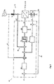
- FIG. 1 shows a three-phase, three-point pulse rectifier system 1 shown, whose basic function in the transformation of a Phase AC voltage sources 2, 3, 4 symbolized three-phase Voltage system 5 in a series connection of the output capacitors 6 and 7 DC voltage occurs.
- the input part of the system is arranged by in each phase Ballast inductors 8, 9 and 10 formed. That of the network side facing terminals of this magnetic energy storage are on connecting lines 11, 12, 13 to the AC side Terminals 14, 15, 16 of a three-phase diode bridge circuit 17 performed, the anode side indirectly to the Terminals 14, 15, 16 lying valves connected on the cathode side 18, 19, 20 via the one forming the positive output voltage rail Connection line 21 to the positive pole 22 of the output capacitor series circuit and the positive output voltage terminal 23 interconnected and their connected on the anode side, Valves located indirectly on terminals 14, 15, 16 on the cathode side 24, 25, 26 over which the negative output voltage rail connecting line 27 forming the negative pole 28 of the output capacitor series circuit and the negative output voltage terminal 29 are connected.
- the leading state and thus the image the output voltage to the input side of the three-phase bridge circuit 17 or the formation of the mains currents of the rectifier is influenced by switches 30, 31, 32.
- the electronic Circuit breakers 30, 31, 32 are in the three-phase diode bridge 17 integrated.
- the collector terminal is in every phase 77 or 79 or 81 of a unidirectional, unipolar, Power semiconductor 61 that can be switched off with the anode on the cathode side lying on the positive output voltage rail 21 Diode 18 or 19 or 20 and the emitter terminal 78 or 80 or 82 with the cathode of the anode side on the negative output voltage rail 27 lying diode 24 or 25 or 26 connected.
- the circuit breakers 30, 31, 32 are each formed by the Power semiconductors 61 that can be switched off, between the DC voltage side Output terminals 77 and 78, or 79 and 80, or 81 and 82 of a single-phase diode bridge circuit 60 is.
- the poles of the switches 30, 31, 32 are defined by the AC-side terminals 14, 15, 16, or those in one Star point 33 interconnected terminals are formed.
- the star point 33 is connected to the Center connection 35 of the series-connected capacitors 6, 7 connected.
- the output voltage is based on the output terminals 23 and 29 one over the connecting lines 37 and 38 consumer circuit 39 supplied.
- a control unit 40 is next to an external control signal 41 combined into a three-pole connecting line 42 Connecting lines 44, 45, 46 the mains phase voltages, the output midpoint voltage via the connecting line 47 and via the connecting line 48 the measured value of the output voltage supplied, with another external, multipole input 49, for example when realizing a current limitation, also the value of the output current or measured values of the switch currents can be included (for reasons of clarity not shown in Fig. 1).
- the system is advantageously controlled in such a way that the Terminals 14, 15, 16 pulse width modulated, with positive (physical current flow leading to the root points) between the Voltage level of the positive output voltage rail 21 and Voltage of the midpoint 35 of the output voltage changing and with physically negative mains current between the voltage level the negative output voltage rail 27 and the voltage the center 35 of the output voltage changing, accordingly the phase shift of the assigned line phase voltages 2, 3, 4 offset voltages are formed.
- the pulse width modulation of the, via control lines 50 (see Fig. 3) the control switches supplied to the electronic switches 30, 31, 32 is done taking into account the through the the series inductances 8, 9, 10 difference of Mains phase voltages and the terminals (14, 15, 16) voltages are impressed Mains phase current flow, which to minimize the Grid load advantageously largely sinusoidal and with respect the fundamental oscillation is in phase with the mains phase voltages is regulated.
- the active power flow resulting from the line phase currents is via the diodes 18, 19, 20, 24, 25, 26 and the electronic Switches 30, 31, 32 switched to the output, whereby the level of the output voltage occurring between terminals 22 and 28 by the amplitude of the mains currents (and thus ultimately through the terminal voltages defined by the control unit) and the load on the output by the DC voltage consumer 39 is determined.
- the center 35 of the Output voltage is via the series connection of output capacitors 6 and 7 are formed, furthermore by these capacitors Differences in the fed in and the consumer side required power flow balanced.
- 2a and 2b are further possible designs of the electronic switches 30, 31, 32 via a combination of power semiconductor elements specified.
- 2c shows for comparison the switch version used in Fig. 1.
- GTO Gate-Turn-Off Thyristor
- Fig. 2b shows an anti-parallel connection of two unidirectional via series combination of a diode 54 or 55 and IGBTs 56 or 57 (IGBT: Insulated Gate Bipolar Transistor) Switching elements 58 and 59 formed embodiment.
- IGBT Insulated Gate Bipolar Transistor
- Fig. 2c there is only one between the (DC side) Output terminals of the single-phase diode bridge circuit 60 switched unidirectional, switchable power semiconductors 61 having embodiment specified.
- the switch poles will through the (AC side) input terminals 62, 63 of the diode bridge circuit 60 is formed.
- the switchable Power semiconductors can also be asymmetrical blocking GTO, a bipolar transistor or a MOSFET replaced become.
- Fig. 3 shows the block diagram of an advantageous embodiment of the control unit, which is only shown schematically in FIG. 1 40.
- the power section is in the form of a single strand Equivalent circuit diagram 64 entered, with the reference numerals of the elements again with those already in connection with the description chosen from Fig. 1 match.
- double lines characterize the combination of three phase signals, ie the transition to a vector representation, which improves clarity the display should be increased.
- the control unit is responsible for regulating the output voltage and the balancing of the output capacitors 6 and 7 occurring partial output voltages.
- the output voltage regulation is double-loop due to a superimposed output voltage control loop 65 and a subordinate current control loop 66 executed.
- the one by an external adjustment device via the Signal line 41 predetermined setpoint related, by a comparison point 67 formed deviation of the output voltage is fed to a control element 68, at whose output the instantaneous value the setpoint of the amplitude of the phase currents and by multiplying by, from the line phase voltages derived signals supplied via the signal line 42 by means of a multiplier 69 into the mains phase current setpoints is reshaped.
- These mains current setpoints are via a Summation point 70 to the the target-actual difference of the phase currents forming comparator 71.
- the difference signal forms the input of a hysteresis switching element 72, at the Output corresponding to the entered switching characteristics pulse width modulated phase switching signals occur which by a functional unit 53 into that of the converter circuit 1 via the control line 50 control commands electronic switch 30, 31 and 32 is formed.
- the through circuit part taken into account function block 53 doing the job of formulating those components of, for example of a triple of binary control commands present by the hysteresis switching element 72 invert control vector formed, which one with respect to the positive count direction 73 negative Grid phase voltage instantaneous value assigned phase are.
- the current control 66 can be influenced the current control 66 via a depending on the asymmetry of the partial output voltages occurring across the capacitors 6 and 7 formed by the comparison element 75, by the Control element 76 of the summation point 70, for all Phases same offset signal also a regulation, in particular Balancing, the partial output voltages are made. If the output signal of the control element 76 is positive, the current controller tries to offset the line phase currents accordingly set which due to the free network star point and thus the amount of electricity forced to 0, however cannot occur.
- Fig. 4 shows a possible modification of that contained in Fig. 1 Power section of the circuit.
- the electronic circuit breakers 30, 31, 32 are not in the three-phase diode bridge 17 integrated.
- the module shown represents an implementation of the one in FIG Dashed lines outlined circuit part, i.e. one Branch 121 of the three-phase circuit arrangement DC parallel connection of three such modules the overall circuit shown in FIG. 7 is realized. It should be ensured that the Parallel connection of the modules is carried out with little inductance.
- One possible implementation for external module connections is EP-A-0 427 340 can be found. There is for external module connections a so-called strip line geometry chosen, the wave resistance with the characteristic impedance of internal module cables matches.
- the circuit shown in FIG. 7 corresponds to that shown in FIG. 1 Power section of the overall circuit.
- Such a low-inductance connection is e.g. in the case a current commutation, for example of transistor 107 the freewheeling diodes 101 and 104 are important. From Fig. 6 is also the desirable spatial close arrangement of two electrical transistors 107 connected in parallel can be seen. By doing 6 are the comb-like manufacturing step Ports 117 have not yet been bent towards the top of the module.
Landscapes
- Engineering & Computer Science (AREA)
- Power Engineering (AREA)
- Rectifiers (AREA)
Description
- daß die elektronischen Schalter in die Drehstrom-Diodenbrücke integriert sind, wobei die Drehstrom-Diodenbrücke durch von den Klemmen der Leistungshalbleiter abzweigende Dioden gebildet ist und
- daß die jeweils zweiten wechselspannungsseitigen Klemmen der elektronischen Schalter in einem Sternpunkt zusammengeschaltet sind, wobei der Mittelanschluß der seriengeschalteten Kondensatoren - abgesehen von Meßleitungen - ausschließlich mit diesem Stempunkt verbunden ist.
- Gegen-Serienschaltung zweier unidirektionaler elektronischer Schalter bzw. Leistungshalbleiter (beispielsweise von MOSFETs oder IGBTs) mit antiparalleler Freilaufdiode,
- die Aniparallelschaltung symmetrisch sperrender GTOs,
- die Antiparallelschaltung von Bipolartransistoren oder IGBTs mit Seriendiode oder durch
- Anordnung eines unidirektionalen elektronischen Schalters zwischen den Ausgangsklemmen einer Einphasen-Diodenbrückenschaltung, deren Eingangsklemmen die Schalterpole bilden,
- Fig. 1
- Struktur einer bevorzugten Ausführung des erfindungsgemäßen Dreiphasen-Dreipunkt-Pulsgleichrichters;
- Fig. 2a bis 2c
- alternative Ausführungsformen bidirektionaler elektronischer Schalter für den Einsatz im Dreiphasen-Dreipunkt-Pulsgleichrichter in entsprechender Schaltungsstruktur;
- Fig. 3
- die Grundstruktur einer Ausführungsvariante des Steuerteiles der erfindungsgemäßen Stromrichterschaltung, die eine Symmetrierung der Ausgangsteilspannungen über Einbeziehung eines Korrektursignales in die, der Ausgangsspannungsregelung unterlagerte Phasenstromregelung erlaubt;
- Fig. 4
- die Grundstruktur des Leistungsteiles des erfindungsgemäßen Systems bei Einsatz der in Fig. 2(c) angegebenen Ausführungsform der bidirektionalen elektronischen Schalter, die auch in Fig. 1 eingesetzt ist, aber in Abwandlung der Struktur gemäß Fig. 1;
- Fig. 5
- Realisierungsform eines Brückenzweigs aus Fig. 1 bzw. Fig. 7 als Modul;
- Fig. 6
- bestücktes Substrat des Moduls gemäß Fig. 5;
- Fig. 7
- der Modulausführung zugrundeliegende elektrische Schaltung.
- 1
- Dreiphasen-Dreipunkt-Pulsgleichrichtersystem
- 2, 3, 4
- Wechselspannungsquelle
- 5
- dreiphasiges Spannungssystem
- 6, 7
- Ausgangskondensator
- 8, 9, 10
- Vorschaltinduktivität
- 11, 12, 13
- Verbindungsleitung
- 14, 15, 16
- wechselspannungsseitige Klemme
- 17
- dreiphasige Diodenbrückenschaltung
- 18, 19, 20
- kathodenseitig verbundene Diode
- 21
- Verbindungsleitung
- 22
- positiver Pol der Serienschaltung der Kondensatoren 6, 7
- 23
- positive Ausgangsklemme
- 24. 25. 26
- anodenseitig verbundene Dioden
- 27
- Verbindungsleitung
- 28
- negativer Pol der Serienschaltung der Kondensatoren 6, 7
- 29
- negative Ausgangsklemme
- 30, 31, 32
- Schalter
- 33
- Sternpunkt, bzw. miteinander verbundene Klemmen
- 34
- Verbindungsleitung
- 35
- Mittelanschluß der seriengeschalteten Kondensatoren 6, 7
- 36, 37, 38
- Verbindungsleitung
- 39
- Verbraucher
- 40
- Steuereinheit
- 41
- externes Steuersignal
- 42
- dreipolige Verbindungsleitung (Signalleitung)
- 43
- -
- 44, 45, 46
- Verbindungsleitung
- 47, 48
- Meßleitung
- 49
- externer mehrpoliger Eingang
- 50
- Steuerleitungen
- 51
- symmetrisch sperrender GTO
- 52
- -
- 53
- Funktionseinheit (Funktionsblock)
- 54, 55
- Diode
- 56, 57
- IGBT
- 58, 59
- Schaltelement
- 60
- Einphasen-Diodenbrückenschaltung
- 61
- abschaltbarer Leistungshalbleiter
- 62, 63
- wechselspannungsseitige Eingangsklemmen der Diodenbrücke 60
- 64
- einsträngiges Ersatzschaltbild des Leistungsteils
- 65
- Ausgangsspannungsregelschleife
- 66
- Stromregelschleife
- 67
- Vergleichsstelle
- 68
- Regelelement
- 69
- Multiplizierglied
- 70
- Summationspunkt
- 71
- Vergleichsstelle
- 72
- Hystereseschaltglied
- 73
- positive Zählrichtung (Spannung)
- 74
- positive Zählrichtung (Strom)
- 75
- Vergleichselement
- 76
- Regelelement
- 77 bis 82
- gleichspannungsseitige Ausgangsklemmen
- 83 bis 100
- -
- 101 bis 107
- Leistungshalbleiterbauelemente
- 108 bis 114
- Anschlüsse
- 115
- Kupferfläche
- 116
- Drahtbonds
- 117
- Anschlüsse
- 118
- Gehäuse
- 119
- Substrat
- 120
- Modul
- 121
- Brückenzweig
Claims (7)
- Vorrichtung zur Umformung eines dreiphasigen Spannungssystems (5) in eine vorgebbare, einen Verbraucher (39) speisende Gleichspannung, welche mittels einer über Vorschaltinduktivitäten (8, 9, 10) an ein Wechselspannungsnetz (2, 3, 4) gelegten Drehstrom-Diodenbrücke (17), einer die Verbraucherspannung stützenden Serienschaltung von Kondensatoren (6, 7) und mittels elektronischer Schalter (30, 31, 32) eine weitgehend sinusförmige Netzstromaufnahme erreicht, wobeia) die elektronischen Schalter (30, 31, 32) durch eine Anordnung unidirektionaler, abschaltbarer, zwischen den gleichspannungsseitigen Klemmen (77 bis 82) von Einphasen-Diodenbrückenschaltungen (60) liegende Leistungshalbleiter (61) ausgeführt sind,b) die Schalterpole der elektronischen Schalter (30, 31, 32) durch die Wechselspannungsklemmen (14, 15, 16 und jeweils 33) gebildet sind,c) je eine wechselspannungsseitige Klemme (14, 15, 16) der elektronischen Schalter (30, 31, 32) mit einer der Vorschaltinduktivitäten (8, 9, 10) verbunden ist,d) die elektronischen Schalter (30, 31, 32) durch eine Steuereinrichtung (40) gesteuert sind, deren Eingangssignale aus der dreiphasigen Wechselspannung, der Ausgangs-Gleichspannung, dem Eingangsstrom, dem Ausgangsstrom und vorgegebenen Sollwerten gebildet und ausgewählt sind,
dadurch gekennzeichnet.e) daß die elektronischen Schalter (30, 31, 32) in die Drehstrom-Diodenbrücke (17) integriert sind, wobei die Drehstrom-Diodenbrücke (17) durch von den Klemmen (77 bis 82) der Leistungshalbleiter (61) abzweigende Dioden (18 bis 20 und 24 bis 26) gebildet ist undf) daß die jeweils zweiten wechselspannungsseitigen Klemmen (33) der elektronischen Schalter (30, 31, 32) in einem Sternpunkt zusammengeschaltet sind, wobei der Mittelanschluß (35) der seriengeschalteten Kondensatoren (6, 7) - abgesehen von Meßleitungen (47) - ausschließlich mit diesem Sternpunkt (33) verbunden ist. - Vorrichtung nach Anspruch 1, dadurch gekennzeichnet, daß die elektronischen Schalter (30, 31, 32) durch eine Gegenserienschaltung zweier unidirektionaler, abschaltbarer Leistungshalbleiter mit antiparalleler Freilaufdiode, z.B. Leistungs-MOS-FETs, gebildet sind.
- Vorrichtung nach Anspruch 1, dadurch gekennzeichnet, daß die elektronischen Schalter (30, 31, 32) durch eine Antiparallelschaltung unidirektionaler, abschaltbarer Leistungshalbleiter, z.B. symmetrisch sperrende GTOs, gebildet sind.
- Vorrichtung nach einem der Ansprüche 1 bis 3, dadurch gekennzeichnet, daß wenigstens ein mit Leistungshalbleiter-Bauelementen (101 bis 107) gebildeter Schaltungsteil, der wenigstens einen Brückenzweig (121) bildet, als Leistungshalbleitermodul (120) ausgeführt ist, wobei durch geeignete Anordnung der Leistungshalbleiter-Bauelemente (101 bis 107) und kurze modulinterne Verbindungsleitungen (115, 116) ein Aufbau mit geringen parasitären Induktivitäten erreicht ist.
- Vorrichtung nach Anspruch 4, dadurch gekennzeichnet, daß zur Bildung des gesamten Leistungshalbleiter-Schaltungsteils drei Leistungshalbleitermodule (120), die jeweils einen Brückenzweig (121) repräsentieren, gleichspannungsseitig parallelgeschaltet sind, wobei induktivitätsarme Verbindungselemente verwendet sind, die aus breiten Bändern mit geringem Abstand zueinander bestehen.
- Verfahren zur Steuerung und Regelung einer Vorrichtung zur Umformung eines dreiphasigen Spannungssystems (5) in eine vorgebbare, einen Verbraucher (39) speisende Gleichspannung, welche mittels einer über Vorschaltinduktivitäten (8, 9, 10) an ein Wechselspannungsnetz (2, 3, 4) gelegten Drehstrom-Diodenbrücke (17), einer die Verbraucherspannung stützenden Serienschaltung von Kondensatoren (6, 7) und mittels elektronischer Schalter (30, 31' 32) eine weitgehend sinusförmige Netzstromaufnahme erreicht, wobeidadurch gekennzeichnet, daß die Steuersignale durch einen auch das Vorzeichen der Netzphasenspannungen erfassenden Funktionsblock (53) derart modifiziert werden, daß unabhängig vom Vorzeichen der Netzspannungen bei Überschreiten einer Schwelle eines Hysteresegliedes (72) in der zugehörigen Phase eine Änderung des Schaltzustandes des jeweiligen elektronischen Schalters (30,31,32) im Sinne einer betragsmäßigen Verkleinerung der Phasenstrom-Regelabweichung vorgenommen wird.die elektronischen Schalter (30, 31' 32) durch eine Steuereinrichtung (40) gesteuert sind, deren Eingangssignale gebildet und ausgewählt sind aus der dreiphasigen Wechselspannung, derAusgangs-Gleichspannung, dem Eingangsstrom, dem Ausgangsstrom und vorgegebenen Sollwerten,die Bildung der den elektronischen Schaltern (30, 31' 32) über Steuerleitungen (50) zugeführten Ansteuersignale durch die Steuereinheit entsprechend der Funktion einer zweischleifigen Regelung der Ausgangsspannung der Vorrichtung erfolgt,der durch externe Einstellvorrichtungen vorgegebene Sollwert der Ausgangsspannung mittels einer Vergleichsstelle (67) mit dem über eine Signalleitung (48) zugeführten Istwert der Ausgangsspannung verglichen und das Ergebnis des Vergleiches an den Eingang eines Regelelementes (68) gelegt und dessen Ausgangssignal über ein Multiplizierglied (69) mit von den Netzphasenspannungen abgeleiteten Signalen zur Berechnung der Netz-Phasenstromsollwerte einer unterlagerten Stromregelschleife (66) herangezogen wird,die Regeldifferenzen der Phasenstrom-Sollwerte durch eine die Strom-Istwerte über Signalleitungen (49) erfassende Vergleichsstelle (71) gebildet und durch Hystereseschaltglieder (72) in pulsbreitenmodulierte Steuersignale umgeformt werden,
- Verfahren nach Anspruch 6, dadurch gekennzeichnet, daß zur Regelung des Potentials des kapazitiven Ausgangsspannungsmittelpunktes (35) der Vorrichtung (1) mit Hysteresestromregelung den Hystereseschaltgliedern (72) zugeführten Sollwerten ein für alle Phasen gleiches, in Abhängigkeit der Asymmetrie der Ausgangsteilspannungen gebildetes Offsetsignal überlagert wird, welches bei Überwiegen der Spannung des ersten Ausgangskondensators (6) gegenüber der Spannung des zweiten Ausgangskondensators (7) während der positiven Netzphasenspannungs- bzw. Netzphasenstromhalbschwingungen die Einschaltdauern der elektronischen Schalter der zugeordneten Phasen verlängert und innerhalb der negativen Halbschwingungen verkürzt, und über den damit auftretenden Mittelwert des in den beiden Kondensatoren (6,7) gemeinsamen Punkt (35) gespeisten Stromes eine Verringerung der Asymmetrie herbeiführt, wobei bei Überwiegen der Spannung des zweiten Kondensators (7) gegenüber der Spannung des ersten Kondensators (6) eine gegensinnige Beeinflussung des resultierend in den Knotenpunkt (35) gespeisten Stromes vorgenommen wird.
Applications Claiming Priority (3)
| Application Number | Priority Date | Filing Date | Title |
|---|---|---|---|
| AT261293 | 1993-12-23 | ||
| AT2612/93 | 1993-12-23 | ||
| AT0261293A AT406434B (de) | 1993-12-23 | 1993-12-23 | Vorrichtung zur umformung eines dreiphasigen spannungssystems in eine vorgebbare, einen verbraucher speisende gleichspannung |
Publications (3)
| Publication Number | Publication Date |
|---|---|
| EP0660498A2 EP0660498A2 (de) | 1995-06-28 |
| EP0660498A3 EP0660498A3 (de) | 1996-06-12 |
| EP0660498B1 true EP0660498B1 (de) | 2003-03-19 |
Family
ID=3537381
Family Applications (1)
| Application Number | Title | Priority Date | Filing Date |
|---|---|---|---|
| EP94120245A Expired - Lifetime EP0660498B1 (de) | 1993-12-23 | 1994-12-20 | Vorrichtung und Verfahren zur Umformung von Drehstrom in Gleichstrom |
Country Status (3)
| Country | Link |
|---|---|
| EP (1) | EP0660498B1 (de) |
| AT (1) | AT406434B (de) |
| DE (1) | DE59410258D1 (de) |
Cited By (2)
| Publication number | Priority date | Publication date | Assignee | Title |
|---|---|---|---|---|
| EP3501885A1 (de) | 2017-12-19 | 2019-06-26 | Dr.Ing. h.c. F. Porsche Aktiengesellschaft | Leistungselektronikmodul für eine ladestation sowie entsprechende ladestation und stromtankstelle |
| DE102019201706A1 (de) * | 2019-02-11 | 2020-08-13 | Vitesco Technologies GmbH | Fahrzeugseitige Ladeschaltung |
Families Citing this family (27)
| Publication number | Priority date | Publication date | Assignee | Title |
|---|---|---|---|---|
| JP2857094B2 (ja) * | 1995-12-28 | 1999-02-10 | 株式会社東芝 | 三相整流装置 |
| AT409569B (de) * | 1999-05-17 | 2002-09-25 | Ascom Energy Systems Ag | Vorrichtung und verfahren zur netzspannungsabhängig thyristorgesteuerten vorladung der ausgangskondensatoren eines dreipunkt-pulsgleichrichtersystems |
| WO2005006531A1 (ja) * | 2003-07-15 | 2005-01-20 | Mitsubishi Denki Kabushiki Kaisha | 三相電力変換装置および電力変換装置 |
| WO2005043742A2 (en) | 2003-10-30 | 2005-05-12 | The Regents Of The University Of California | Universal three phase controllers for power converters |
| CN100356672C (zh) * | 2003-12-29 | 2007-12-19 | 艾默生网络能源有限公司 | 三相功率因数校正电能变换装置 |
| US7751212B2 (en) | 2007-04-23 | 2010-07-06 | Raytheon Company | Methods and apparatus for three-phase rectifier with lower voltage switches |
| JP5167884B2 (ja) | 2008-03-14 | 2013-03-21 | ダイキン工業株式会社 | コンバータの制御方法及び制御装置 |
| EP2259420A1 (de) * | 2009-06-02 | 2010-12-08 | ABB Research Ltd. | Einphasen-Wechselrichter |
| JP4687824B2 (ja) * | 2009-06-26 | 2011-05-25 | 株式会社富士通ゼネラル | 3相整流器 |
| CN102783007B (zh) * | 2010-03-31 | 2015-08-05 | 日立空调·家用电器株式会社 | 转换器装置、马达驱动用模块以及冷冻机 |
| SE536410C2 (sv) | 2010-10-12 | 2013-10-15 | Ferroamp Elektronik Ab | Anordning för begränsning av en elektrisk ström |
| US9252670B2 (en) | 2012-12-19 | 2016-02-02 | General Electric Company | Multilevel converter |
| DK3068024T3 (en) * | 2015-03-09 | 2018-04-23 | Siemens Ag | Procedure for controlling a Vienna rectifier |
| FR3067886B1 (fr) * | 2017-06-15 | 2023-05-26 | Nissan Motor | Procede de commande d'un redresseur de vienne triphase |
| FR3082678B1 (fr) | 2018-06-15 | 2020-05-22 | Renault S.A.S | Procede de commande d'un redresseur de vienne. |
| US10944319B2 (en) | 2018-11-30 | 2021-03-09 | Schneider Electric It Corporation | Flying battery with AC switch PFC front end for ups |
| DE102019106485B4 (de) * | 2019-03-14 | 2021-04-08 | Dr. Ing. H.C. F. Porsche Aktiengesellschaft | Weissach-Gleichrichteranordnung |
| US11664722B2 (en) | 2019-12-05 | 2023-05-30 | Abb Power Electronics Inc. | Technologies for controlling AC-to-DC converters |
| WO2021144234A1 (de) * | 2020-01-13 | 2021-07-22 | Convertertec Deutschland Gmbh | Verfahren zum phasengetrennten überstromschutz einer dreiphasigen brückenschaltung |
| DE102020119104B3 (de) | 2020-07-21 | 2021-09-16 | Dr. Ing. H.C. F. Porsche Aktiengesellschaft | Gleichrichteranordnung |
| DE102020119105A1 (de) | 2020-07-21 | 2022-01-27 | Dr. Ing. H.C. F. Porsche Aktiengesellschaft | Gleichrichteranordnung |
| DE102020129247A1 (de) | 2020-11-06 | 2022-05-12 | Dr. Ing. H.C. F. Porsche Aktiengesellschaft | Gleichrichteranordnung |
| CN112271940B (zh) * | 2020-11-10 | 2024-07-12 | 中国矿业大学(北京) | 一种具有公共高压直流母线的五电平整流器及控制策略 |
| CN117353566A (zh) * | 2022-06-29 | 2024-01-05 | 佛山市顺德区美的电子科技有限公司 | 家电设备的三相电源变换电路、家电设备和上电控制方法 |
| FI131169B1 (en) | 2022-08-09 | 2024-11-15 | Lappeenrannan Lahden Teknillinen Yliopisto Lut | System and method of an electrochemical process |
| EP4654455A1 (de) | 2024-05-22 | 2025-11-26 | Diehl AKO Stiftung & Co. KG | Elektronische schaltung mit zwei zwischenkreisen, verfahren, leistungsmodul und elektrische vorrichtung |
| CN120468566B (zh) * | 2025-07-08 | 2025-09-23 | 中科兆和电力技术(山东)有限公司 | 一种矿热炉用供电功率模块测试系统 |
Family Cites Families (6)
| Publication number | Priority date | Publication date | Assignee | Title |
|---|---|---|---|---|
| DE2419222A1 (de) * | 1974-04-22 | 1975-10-30 | Hans Werner Johannsen | Spiralklammer |
| DE3127457C2 (de) * | 1981-07-11 | 1985-09-12 | Brown, Boveri & Cie Ag, 6800 Mannheim | Stromrichtermodul |
| DE3241508A1 (de) * | 1982-11-10 | 1984-05-10 | Brown, Boveri & Cie Ag, 6800 Mannheim | Leistungstransistor-modul |
| FR2564259B1 (fr) * | 1984-05-09 | 1986-09-19 | Commissariat Energie Atomique | Amplificateur a decoupage |
| DE3937045A1 (de) * | 1989-11-07 | 1991-05-08 | Abb Ixys Semiconductor Gmbh | Leistungshalbleitermodul |
| AT403865B (de) * | 1991-07-10 | 1998-06-25 | Fronius Schweissmasch | Spannungsumsetzungsvorrichtung für einen gleichspannungsverbraucher |
-
1993
- 1993-12-23 AT AT0261293A patent/AT406434B/de not_active IP Right Cessation
-
1994
- 1994-12-20 EP EP94120245A patent/EP0660498B1/de not_active Expired - Lifetime
- 1994-12-20 DE DE59410258T patent/DE59410258D1/de not_active Expired - Lifetime
Cited By (2)
| Publication number | Priority date | Publication date | Assignee | Title |
|---|---|---|---|---|
| EP3501885A1 (de) | 2017-12-19 | 2019-06-26 | Dr.Ing. h.c. F. Porsche Aktiengesellschaft | Leistungselektronikmodul für eine ladestation sowie entsprechende ladestation und stromtankstelle |
| DE102019201706A1 (de) * | 2019-02-11 | 2020-08-13 | Vitesco Technologies GmbH | Fahrzeugseitige Ladeschaltung |
Also Published As
| Publication number | Publication date |
|---|---|
| DE59410258D1 (de) | 2003-04-24 |
| EP0660498A3 (de) | 1996-06-12 |
| ATA261293A (de) | 1999-09-15 |
| AT406434B (de) | 2000-05-25 |
| EP0660498A2 (de) | 1995-06-28 |
Similar Documents
| Publication | Publication Date | Title |
|---|---|---|
| EP0660498B1 (de) | Vorrichtung und Verfahren zur Umformung von Drehstrom in Gleichstrom | |
| DE10103031B4 (de) | Stromrichterschaltung mit verteilten Energiespeichern und Verfahren zur Steuerung einer derartigen Stromrichterschaltung | |
| DE69327353T2 (de) | Regeleinrichtung für ein Hochspannungs-Gleichstromübertragungssystem | |
| EP3211784B1 (de) | Doppel-submodul für einen modularen mehrpunktstromrichter und modularer mehrpunktstromrichter mit diesem | |
| DE112008001796B4 (de) | Wechselrichtersystem und Steuerverfahren | |
| WO2007033852A2 (de) | Verfahren zur steuerung eines mehrphasigen stromrichters mit verteilten energiespeichern | |
| EP0299339A1 (de) | Vorrichtung zur verlustarmen Beschaltung der Halbleiterschaltelemente eines Dreipunktwechselrichters | |
| EP1336242A2 (de) | Verfahren zur steuerung eines matrixumrichters | |
| DE10153738B4 (de) | Gleichrichterschaltung und Verfahren zu deren Steuerung | |
| DE19829856A1 (de) | Dreipunkt-Stromrichter und Verfahren zum Betrieb | |
| EP1245074B1 (de) | Netzrückwirkungsarmes dreiphasen-stromzwischenkreis-pulsgleich-richtersystem mit weitem stellbereich der ausgangsspannung | |
| EP2807738B1 (de) | Multizellenkonverter | |
| DE69610000T2 (de) | Leistungswandler | |
| EP3605821B1 (de) | Selbstgeführter direktumrichter und ansteuerverfahren für selbstgeführten direktumrichter | |
| WO2009156021A1 (de) | Spannungswandlerschaltung und wechselrichter | |
| EP1137160B1 (de) | Stromrichterschaltung | |
| EP3806314B1 (de) | Umrichter für ein wechselstromnetz | |
| WO2013186006A2 (de) | Multizellenkonverter | |
| EP2409394B1 (de) | Verfahren zum betrieb einer umrichterschaltung sowie vorrichtung zur durchführung des verfahrens | |
| DE3831126C2 (de) | Wechselrichter mit eingeprägter Zwischenkreisspannung | |
| DE102022119531B4 (de) | Stromrichtereinrichtung mit einem Stromrichter und mit einer Steuereinrichtung | |
| DE19942258A1 (de) | Schaltung und Verfahren zur Einschaltentlastung von abschaltbaren Leistungsschaltern in Dreipunkt-Stromrichtern | |
| AT404527B (de) | Aktive netzspannungsfilterung mit vorgebbarer innerer impedanz | |
| DE102007046511B4 (de) | Stromrichter mit unterbrechbarem Parallelkreis und Umrichter mit zwei parallelkreis-unterbrechenden Stromrichtern | |
| EP1011189B1 (de) | Verfahren und Schaltungsanordnung zur Anpassung der Zwischenkreisspannung an die Versorgungsspannung |
Legal Events
| Date | Code | Title | Description |
|---|---|---|---|
| PUAI | Public reference made under article 153(3) epc to a published international application that has entered the european phase |
Free format text: ORIGINAL CODE: 0009012 |
|
| AK | Designated contracting states |
Kind code of ref document: A2 Designated state(s): DE FR GB IT |
|
| PUAL | Search report despatched |
Free format text: ORIGINAL CODE: 0009013 |
|
| AK | Designated contracting states |
Kind code of ref document: A3 Designated state(s): DE FR GB IT |
|
| 17P | Request for examination filed |
Effective date: 19960610 |
|
| 17Q | First examination report despatched |
Effective date: 19970707 |
|
| GRAG | Despatch of communication of intention to grant |
Free format text: ORIGINAL CODE: EPIDOS AGRA |
|
| GRAG | Despatch of communication of intention to grant |
Free format text: ORIGINAL CODE: EPIDOS AGRA |
|
| GRAH | Despatch of communication of intention to grant a patent |
Free format text: ORIGINAL CODE: EPIDOS IGRA |
|
| GRAH | Despatch of communication of intention to grant a patent |
Free format text: ORIGINAL CODE: EPIDOS IGRA |
|
| GRAA | (expected) grant |
Free format text: ORIGINAL CODE: 0009210 |
|
| AK | Designated contracting states |
Designated state(s): DE FR GB IT |
|
| REG | Reference to a national code |
Ref country code: GB Ref legal event code: FG4D Free format text: NOT ENGLISH |
|
| REF | Corresponds to: |
Ref document number: 59410258 Country of ref document: DE Date of ref document: 20030424 Kind code of ref document: P |
|
| GBT | Gb: translation of ep patent filed (gb section 77(6)(a)/1977) |
Effective date: 20030429 |
|
| ET | Fr: translation filed | ||
| PLBE | No opposition filed within time limit |
Free format text: ORIGINAL CODE: 0009261 |
|
| STAA | Information on the status of an ep patent application or granted ep patent |
Free format text: STATUS: NO OPPOSITION FILED WITHIN TIME LIMIT |
|
| 26N | No opposition filed |
Effective date: 20031222 |
|
| REG | Reference to a national code |
Ref country code: DE Ref legal event code: R082 Ref document number: 59410258 Country of ref document: DE Representative=s name: OPPERMANN, FRANK, DIPL.-ING., DE Ref country code: DE Ref legal event code: R082 Ref document number: 59410258 Country of ref document: DE Representative=s name: FRANK OPPERMANN, DE |
|
| PGFP | Annual fee paid to national office [announced via postgrant information from national office to epo] |
Ref country code: DE Payment date: 20131213 Year of fee payment: 20 Ref country code: GB Payment date: 20131209 Year of fee payment: 20 |
|
| PGFP | Annual fee paid to national office [announced via postgrant information from national office to epo] |
Ref country code: FR Payment date: 20131126 Year of fee payment: 20 Ref country code: IT Payment date: 20131216 Year of fee payment: 20 |
|
| REG | Reference to a national code |
Ref country code: DE Ref legal event code: R071 Ref document number: 59410258 Country of ref document: DE |
|
| REG | Reference to a national code |
Ref country code: DE Ref legal event code: R071 Ref document number: 59410258 Country of ref document: DE |
|
| REG | Reference to a national code |
Ref country code: GB Ref legal event code: PE20 Expiry date: 20141219 |
|
| PG25 | Lapsed in a contracting state [announced via postgrant information from national office to epo] |
Ref country code: GB Free format text: LAPSE BECAUSE OF EXPIRATION OF PROTECTION Effective date: 20141219 |