EP0660330A2 - Data processing system having a memory with a low power operating mode and method therefor - Google Patents
Data processing system having a memory with a low power operating mode and method therefor Download PDFInfo
- Publication number
- EP0660330A2 EP0660330A2 EP94118906A EP94118906A EP0660330A2 EP 0660330 A2 EP0660330 A2 EP 0660330A2 EP 94118906 A EP94118906 A EP 94118906A EP 94118906 A EP94118906 A EP 94118906A EP 0660330 A2 EP0660330 A2 EP 0660330A2
- Authority
- EP
- European Patent Office
- Prior art keywords
- address
- control
- signal
- memory
- memory array
- Prior art date
- Legal status (The legal status is an assumption and is not a legal conclusion. Google has not performed a legal analysis and makes no representation as to the accuracy of the status listed.)
- Withdrawn
Links
Images


Classifications
-
- G—PHYSICS
- G06—COMPUTING; CALCULATING OR COUNTING
- G06F—ELECTRIC DIGITAL DATA PROCESSING
- G06F13/00—Interconnection of, or transfer of information or other signals between, memories, input/output devices or central processing units
- G06F13/14—Handling requests for interconnection or transfer
-
- G—PHYSICS
- G11—INFORMATION STORAGE
- G11C—STATIC STORES
- G11C8/00—Arrangements for selecting an address in a digital store
-
- G—PHYSICS
- G11—INFORMATION STORAGE
- G11C—STATIC STORES
- G11C11/00—Digital stores characterised by the use of particular electric or magnetic storage elements; Storage elements therefor
- G11C11/21—Digital stores characterised by the use of particular electric or magnetic storage elements; Storage elements therefor using electric elements
- G11C11/34—Digital stores characterised by the use of particular electric or magnetic storage elements; Storage elements therefor using electric elements using semiconductor devices
- G11C11/40—Digital stores characterised by the use of particular electric or magnetic storage elements; Storage elements therefor using electric elements using semiconductor devices using transistors
- G11C11/41—Digital stores characterised by the use of particular electric or magnetic storage elements; Storage elements therefor using electric elements using semiconductor devices using transistors forming static cells with positive feedback, i.e. cells not needing refreshing or charge regeneration, e.g. bistable multivibrator or Schmitt trigger
- G11C11/413—Auxiliary circuits, e.g. for addressing, decoding, driving, writing, sensing, timing or power reduction
- G11C11/417—Auxiliary circuits, e.g. for addressing, decoding, driving, writing, sensing, timing or power reduction for memory cells of the field-effect type
- G11C11/418—Address circuits
Definitions
- This invention relates generally to data processing systems, and more particularly, to a data processing system having a memory with a low power operating mode.
- SRAM static random access memory
- the on-board SRAM may be disabled when it is not being used.
- an access to the SRAM requires that it be re-enabled before the access can occur, which requires the data processing system to wait until the SRAM is reenabled.
- lower power consumption has been achieved in a SRAM by operating the SRAM at a lower clock frequency.
- lowering the clock frequency at which the SRAM operates also affects the operation of the entire data processing system.
- a semiconductor memory having a memory array, an address decoder, and control circuitry.
- the memory array has a plurality of memory cells arranged in rows and columns, each memory cell coupled to a word line and to a bit line.
- the address decoder is coupled to the memory array and accesses a memory cell of the memory array in response to an address signal.
- the control circuitry is coupled to the address decoder and causes the memory cell to be accessed within a first predetermined time in response to a control signal being in a first predetermined logic state.
- the control circuitry causes the memory cell to be accessed within a second predetermined time in response to the control signal being in a second predetermined logic state.
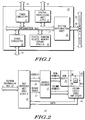
- FIG. 1 illustrates in block diagram form, a data processing system in accordance with one embodiment of the present invention.
- FIG. 2 illustrates in block diagram form, the static random access memory of FIG. 1 in accordance with one embodiment of the present invention.
- FIG. 3 illustrates in block diagram form, the bus interface unit of FIG. 2 in accordance with one of embodiment the present invention.
- FIG. 4 illustrates in block diagram form, the control register of FIG. 3 in accordance with one embodiment of the present invention.
- FIG. 5 illustrates a timing diagram of various signals of the static random access memory of FIG. 2 during a one cycle access mode.
- FIG. 6 illustrates a timing diagram of various signals of the static random access memory of FIG. 2 during a two cycle access mode.
- the present invention provides a low power operating mode for an on-board memory in a data processing system. This is accomplished by providing a programmable control bit for switching from a one clock cycle access mode to a two clock cycle access mode.
- BIU bus interface unit
- the address is compared to determine if the address is a valid SRAM address. If the address is valid, the address decoders are enabled, or activated, and a data transfer is completed on the next cycle. If the address is not valid, the address decoders are not enabled and the memory array remains in a quiescent state consuming minimum power.
- the SRAM decodes every address so that it can respond in one cycle to a valid address.
- the present invention can be more fully described with reference to FIG. 1 - 6.
- assert and “negate” will be used when referring to the rendering of a signal, status bit, or similar apparatus into its logically true or logically false state, respectively. If the logically true state is a digital logic level one, the logically false state will be a digital logic level zero. And if the logically true state is a digital logic level zero, the logically false state will be a digital logic level one.
- bus will be used to refer to a plurality of signals which may be used to transfer one or more various types of information, such as data, addresses, control, or status.
- FIG. 1 illustrates in block diagram form, a data processing system 10 in accordance with one embodiment of the present invention.
- Data processing system 10 can be implemented as a single integrated circuit called a microcontroller.
- Data processing system 10 has various on-board peripherals which are bi-directionally coupled by way of an information bus 22.
- the particular embodiment of data processing system 10 illustrated in FIG. 1 has a central processing unit (CPU) 12, timer circuitry 14, static random access memory (SRAM) 18, other circuitry 16, and system integration unit 20, which are all bi-directionally coupled to information bus 22.
- Other circuitry 16 may include, for example, a read only memory (ROM), an analog-to-digital converter, serial circuitry, or an electrically erasable programmable read only memory (EEPROM).
- ROM read only memory
- EEPROM electrically erasable programmable read only memory
- System integration unit 20 can receive and transmit signals external to data processing system 10 by way of integrated circuit pins 38.
- Integrated circuit pins 38 may optionally be coupled to an external bus 40.
- CPU 12 may optionally receive and transmit signals external to data processing system 10 by way of integrated circuit pins 32.
- Timer circuitry 14 can receive and transmit signals external to data processing system 10 by way of integrated circuit pins 34.
- FIG. 1 illustrates one particular microcontroller within a family of microcontrollers. Because microcontrollers in the same family generally have a plurality of differing on-board peripherals, FIG. 1 provides only one embodiment of data processing system 10. Alternate embodiments of data processing system 10 may have fewer, more, or different on-board peripherals than those illustrated in FIG. 1.
- FIG. 2 illustrates in block diagram form, static random access memory 18 of FIG. 1 in accordance with one embodiment of the present invention.
- SRAM 18 includes bus interface unit (BIU) 41, address decoders 42, row select circuits 45, column logic/sense amplifiers 46, and memory array 43.
- BIU bus interface unit
- BIU 41 is coupled to information bus 22 in order to allow SRAM 18 to communicate with other. portions of circuitry in data processing system 10. For example, BIU 41 may receive address and data signals from CPU 12 across information bus 22, and BIU 41 may transfer data signals back to CPU 12 across information bus 22. BIU 41 transfers address signals to address decoders 42. BIU 41 is also bi-directionally coupled to column logic/sense amplifiers 46 for transferring data signals to and from column logic/sense amplifiers 46. BIU 41 also provides an address decode enable signal 47 for enabling or disabling address decoders 42. Address decode enable signal 47 will be discussed later in more detail in the discussion of FIG. 3.
- Memory array 43 is a conventional SRAM array and includes an array of SRAM cells arranged in rows and columns. Each SRAM cell is coupled to a word line and to a bit line pair. The word lines are connected to row select circuits 45, and the bit line pairs are connected to column logic/sense amplifiers 46.
- a predetermined number of address signals are provided to address decoders 42.
- the predetermined number of address signals includes a row address portion and a column address portion.
- the row address portion is provided to the row select circuit 45 and the column address portion is provided to column logic/sense amplifiers 46.
- the row address is used to select a particular word line and the column address is used to select a particular bit line pair.
- memory array 43 may be subdivided into sections or blocks. Included in SRAM 18, but not shown, are bit line loads, write drivers, bit line precharge and equalization circuitry. A memory cell located at the intersection of a selected word line and bit line pair may be accessed for either a read cycle or a write cycle. A representative memory cell 44 is shown connected to a word line labeled "WL”, and to a bit line pair labeled "BL" and "BL*". Note that an asterisk (*) after a signal or line name indicates that the signal or line is a logical complement of a signal or line having the same name but lacking the asterisk (*).
- a valid address selects a memory cell to be accessed, for example memory cell 44.
- Information is provided by memory cell 44 to bit line pair BL/BL*, in the form of a differential voltage across the bit line pair.
- Sense amplifiers in column logic/sense amplifiers 46 senses and amplifiers the differential voltage and provides the differential voltage to BIU 41.
- a selected bit line pair for example bit line pair BL/BL*, receives the data in the form of a differential voltage, and provides the differential voltage to a memory cell that is coupled to the selected word line and bit line pair.
- SRAM 18 has two modes of operation which are programmable by a user, a normal, or one cycle mode, and a low power, or two cycle mode.
- address decode enable signal 47 is asserted to enable the address decoders on each transaction from information bus 22, so that an access of memory array 43 occurs in one clock cycle to allow high speed operation.
- an access of SRAM 18 requires two clock cycles.
- Address decode enable signal 47 is asserted in the next clock cycle after a valid address is received from information bus 22.
- power consumption is reduced as compared to the one cycle mode of operation. Note that in the illustrated embodiment, during low power mode, an access to memory array 43 occurs in two clock cycles. In other embodiments, an access to memory array 43 may occur in a predetermined time that is different than two clock cycles. Also, in the illustrated embodiment, memory array 43 is an SRAM array.
- memory array 43 may be any other type of volatile or nonvolatile memory array, including but not limited to, dynamic random access memory (DRAM), read only memory (ROM), programmable read only memory (PROM), and electrically erasable programmable read only memory (EEPROM)
- DRAM dynamic random access memory
- ROM read only memory
- PROM programmable read only memory
- EEPROM electrically erasable programmable read only memory
- FIG. 3 illustrates in block diagram form, BIU 41 of FIG. 2 in accordance with one embodiment of the present invention.
- BIU 41 includes address latches 51 and 52, multiplexer 54, address comparator 53, state machine 55, control registers 49, and counter 56.
- Address latch 51 has input terminals coupled to information bus 22, an input terminal for receiving control signal C3, and output terminals coupled to address latch 52, multiplexer 54, and address comparator 53.
- address latch 52 has an input terminal for receiving control signal C1, and output terminals connected to multiplexer 54.
- Address comparator 53 has input terminals for receiving an address from address latch 51, an input terminal for receiving control signal C4, and an output terminal for providing an address match signal labeled "MATCH".
- State machine 55 has an input terminal connected to address comparator 53 for receiving match signal MATCH, an input terminal connected to control registers 49, and an output terminal connected to address decoders 42 for providing decode enable signal 47.
- Control registers 49 has an input terminal connected to counter 56, and an output terminal for providing control bit 57 of control registers 49 to state machine 55 and to multiplexer 54.
- Counter 56 has an input terminal for receiving match signal MATCH from address comparator 53, an input terminal for receiving a transfer start signal labeled "TRANSFER START", and an output terminal connected to control registers 49.
- Control signals C1, C3, and C4 are numbered to correspond to the phase of the clock signal shown in the timing diagrams of FIG. 5 and FIG. 6. FIG. 5 and 6 will be discussed later.
- BIU 41 functions to interface memory array 43 to information bus 22.
- Address latch 51 receives an address from information bus 22 on each clock cycle and provides the address to address latch 52. The address is also provided to address comparator 53 and to multiplexer 54 based on timing information provided by control signals C1, C3, and C4 respectively. Address comparator 53 provides a match signal to state machine 55. Control information is also provided to state machine 55 by control bit 57. Another input to multiplexer 54 is provided by address latch 52.
- control bit 57 is programmed by the user to provide a logic zero to state machine 55 and to multiplexer 54.
- the output of address latch 51 is provided to address decoders 42 on every clock cycle via multiplexer 54.
- address decoder 42 (FIG. 2) is enabled during each clock cycle by decode enable signal 47 from state machine 55. This allows memory array 43 to transfer data to or from BIU 41 in the same cycle that a valid address is received.
- control bit 57 is programmed by the user to provide a logic one to state machine 55 and to multiplexer 54.
- the output of second address latch 52 is provided to address decoders 42 on every clock cycle via multiplexer 54.
- Address decoders 42 are disabled by decode enable signal 47 from state machine 55.
- address comparator 53 determines if the address it receives is a valid address for accessing memory array 43 for a read or a write operation. When a valid address is received, match signal MATCH is asserted by address comparator 53 and provided to state machine 55. During a subsequent cycle, state machine 55 asserts decode enable signal 47.
- Decode enable signal 47 causes address decoders 42 to be enabled, thus accessing the memory array for a read or a write operation. Data is then transferred between BIU 41 and memory array 43. If a valid address is not received, decode enable signal 47 is negated. The address decoders then remain disabled, or inactive, to reduce the power consumption of data processing system 10.
- Counter 56 monitors transfer start signal TRANSFER START from information bus 22 as well as match signal MATCH from address comparator 53. Based on this information, the counter can automatically assert or negate the control bit 57 to automatically change from two cycle mode to one cycle mode or back.
- Counter 56 provides an automatic, self-monitoring mechanism to switch SRAM 18 from one cycle mode to two cycle mode and back to one cycle mode.
- Counter 56 monitors transfer start signal TRANSFER START from information bus 22 and match signal MATCH from address comparator 53 to determine the number of information bus 22 transactions which target SRAM 18. If counter 56 determines that the number of consecutive SRAM 18 accesses falls below a predetermined value, SRAM 18 automatically switches to two cycle mode for reduced power consumption. While in two cycle mode, SRAM 18 may automatically switch to single cycle mode if counter 56 determines that the number of consecutive SRAM 18 accesses rises above the predetermined value.
- the predetermined value may be defined as either a fixed number of consecutive SRAM 18 accesses or as a ratio of SRAM 18 accesses compared with a fixed number of past information bus 22 transactions.
- match signal MATCH from address comparator 53 could simply cause counter 56 to put SRAM 18 into one cycle mode for a predetermined number of assertions of transfer start signal TRANSFER START from information bus 22.
- the predetermined number of cycles could be programmed via a data transfer on information bus 22.
- state machine 55 may be another type of control logic such as a programmable logic array.
- FIG. 4 illustrates in block diagram form, control registers 49 of FIG. 3 in accordance with one embodiment of the present invention.
- Control registers 49 includes 32 control bits. In other embodiments, control registers 49 may include more or fewer control bits.
- Control bit 57 is programmable by the user to provide a predetermined control value, and controls whether memory array 43 is accessed in one clock cycle or two clock cycles. When control bit 57 is asserted, SRAM 18 operates in two cycle mode. When control bit 57 is negated, SRAM 18 operates in one cycle mode. In other embodiments, control bit 57 may include more that one control bit.
- FIG. 5 illustrates a timing diagram of various signals of SRAM 18 of FIG. 2 during one cycle, or normal access mode. Note that the clock signal is divided into four phases per cycle for reference, and each phase is labeled uniquely by "T” followed by a number. Note also that the various signals of FIG. 5 are not drawn to scale.
- a transaction on information bus 22, that is directed to SRAM 18, begins at time T3.
- Address information and transfer start signal TRANSFER START are supplied at time T3.
- Address latch 51 captures addresses from information bus 22 during time T3 in response to control signal C3.
- address comparator 53 begins decoding the address held in address latch 51 to determine if the address is valid for accessing SRAM 18.
- the address information held in address latch 51 is also passed through multiplexer 54 to address decoder 42.
- Address decoder 42 decodes rows and columns in memory array 43 during time T4. If the address is valid, and a read operation is required, the sense amplifiers in column logic/sense amplifiers 46 transfer data from memory array 43 to BIU 41 during times T5 and T6. BIU 41 relays data onto information bus 22 during time T7 if address comparator 53 determines that the information bus 22 transaction targets SRAM 18.
- address comparator 53 determines that the information bus 22 transaction does not target SRAM 18, BIU 41 does not transfer data onto information bus 22. Note that the address held in address latch 51 is decoded by address decoder 42 during time T4, even though the transaction may not have been targeting SRAM 18. This is because address comparator 53 does not have time to determine ownership of the information bus 22 transaction, and still be able to allow an access of SRAM 18 in one clock cycle. Therefore, the rows and columns of memory array 43 are decoded on every active bus cycle so that SRAM 18 is able to respond by the end of the cycle. Decoding each address allows high speed operation of SRAM 18 at the cost of increased power consumption.
- FIG. 6 illustrates a timing diagram of various signals of SRAM 18 of FIG. 2 during a two cycle, or low power access mode. Note that the clock signal illustrated in FIG. 6 is divided into four phases per cycle for reference, and the phases are labeled uniquely by "T" and a number. Note also that the various signals in FIG. 6 are not drawn to scale.
- address latch 51 In two cycle mode, the beginning of the information bus 22 transaction is the same as for a one cycle mode access. Address information from information bus 22 is held at time T3 in address latch 51. The address in address latch 51 is decoded by address comparator 53 during time T4 to determine ownership of the transaction. Address comparator 53 generates match signal MATCH, which is provided to state machine 55 and counter 56 at the end of time T4, if the address in address latch 51 is valid for accessing SRAM 18. The address information in address latch 51 is passed to address latch 52 during time T5 for future use. When match signal MATCH is asserted by address comparator 53, decode enable signal 47 is asserted by state machine 55.
- address stored in address latch 52 is passed through multiplexer 54 to address decoders 42 for row and column decoding at time T8. At times T9 and T10 data is transferred between column logic/sense amplifiers 46 and BIU 18. If a read operation is required, BIU 18 drives data onto information bus 22 at time T11.
- match signal MATCH is not asserted at the end of time T4 by address comparator 53, state machine 55 does not assert decode enable signal 47, and the address information stored in address latch 52 is not passed to address decoder 42 for row and column decoding. Address decoder 42, row select 45, and column logic/sense amplifiers 46 are not enabled and remain in a low power quiescent state, thus reducing the power consumption of data processing system 10.
- address latches 51 and 52 allow for "pipelining" of sequential transactions to SRAM 18.
- the additional clock cycle allows address comparator 53 to determine ownership of an information bus 22 transaction while holding address decoder 42, row select 45, column logic/sense amplifiers 46, and memory array 43 in a low power quiescent state until this circuitry is really needed.
Abstract
Description
- This invention relates generally to data processing systems, and more particularly, to a data processing system having a memory with a low power operating mode.
- Data processing systems, such as microcontrollers, commonly use on-board memory. There are various types of memory used on-board a microcontroller, including both volatile and nonvolatile memory. One type of volatile memory that is used in high speed applications, such as when the microcontroller is used in a workstation, is static random access memory (SRAM). Compared to other types of on-board memory, a SRAM can operate at relatively high access speeds. However, high speed operation generally requires high power consumption, which is undesirable for applications such as battery powered computers, where low power consumption may be more important than high speed operation.
- To reduce power consumption in prior art data processing systems having an on-board SRAM, the on-board SRAM may be disabled when it is not being used. However, an access to the SRAM requires that it be re-enabled before the access can occur, which requires the data processing system to wait until the SRAM is reenabled. Also, lower power consumption has been achieved in a SRAM by operating the SRAM at a lower clock frequency. However, lowering the clock frequency at which the SRAM operates also affects the operation of the entire data processing system.
- Accordingly, there is provided, in one form, a semiconductor memory having a memory array, an address decoder, and control circuitry. The memory array has a plurality of memory cells arranged in rows and columns, each memory cell coupled to a word line and to a bit line. The address decoder is coupled to the memory array and accesses a memory cell of the memory array in response to an address signal. The control circuitry is coupled to the address decoder and causes the memory cell to be accessed within a first predetermined time in response to a control signal being in a first predetermined logic state. The control circuitry causes the memory cell to be accessed within a second predetermined time in response to the control signal being in a second predetermined logic state.
- Also, there is provided, in another form, a method for accessing the memory array. These and other features and advantages will be more clearly understood from the following detailed description taken in conjunction with the accompanying drawings.
- FIG. 1 illustrates in block diagram form, a data processing system in accordance with one embodiment of the present invention.
- FIG. 2 illustrates in block diagram form, the static random access memory of FIG. 1 in accordance with one embodiment of the present invention.
- FIG. 3 illustrates in block diagram form, the bus interface unit of FIG. 2 in accordance with one of embodiment the present invention.
- FIG. 4 illustrates in block diagram form, the control register of FIG. 3 in accordance with one embodiment of the present invention.
- FIG. 5 illustrates a timing diagram of various signals of the static random access memory of FIG. 2 during a one cycle access mode.
- FIG. 6 illustrates a timing diagram of various signals of the static random access memory of FIG. 2 during a two cycle access mode.
- Generally, the present invention provides a low power operating mode for an on-board memory in a data processing system. This is accomplished by providing a programmable control bit for switching from a one clock cycle access mode to a two clock cycle access mode. During two cycle mode, only the bus interface unit (BIU) for the memory is active during each bus transation. During the first cycle of the two cycle access, the address is compared to determine if the address is a valid SRAM address. If the address is valid, the address decoders are enabled, or activated, and a data transfer is completed on the next cycle. If the address is not valid, the address decoders are not enabled and the memory array remains in a quiescent state consuming minimum power. During one cycle mode, the SRAM decodes every address so that it can respond in one cycle to a valid address.
- The present invention can be more fully described with reference to FIG. 1 - 6. The terms "assert" and "negate" will be used when referring to the rendering of a signal, status bit, or similar apparatus into its logically true or logically false state, respectively. If the logically true state is a digital logic level one, the logically false state will be a digital logic level zero. And if the logically true state is a digital logic level zero, the logically false state will be a digital logic level one. The term "bus" will be used to refer to a plurality of signals which may be used to transfer one or more various types of information, such as data, addresses, control, or status.
- FIG. 1 illustrates in block diagram form, a
data processing system 10 in accordance with one embodiment of the present invention.Data processing system 10 can be implemented as a single integrated circuit called a microcontroller.Data processing system 10 has various on-board peripherals which are bi-directionally coupled by way of aninformation bus 22. The particular embodiment ofdata processing system 10 illustrated in FIG. 1 has a central processing unit (CPU) 12,timer circuitry 14, static random access memory (SRAM) 18,other circuitry 16, andsystem integration unit 20, which are all bi-directionally coupled toinformation bus 22.Other circuitry 16 may include, for example, a read only memory (ROM), an analog-to-digital converter, serial circuitry, or an electrically erasable programmable read only memory (EEPROM). -
System integration unit 20 can receive and transmit signals external todata processing system 10 by way of integratedcircuit pins 38.Integrated circuit pins 38 may optionally be coupled to anexternal bus 40.CPU 12 may optionally receive and transmit signals external todata processing system 10 by way of integratedcircuit pins 32.Timer circuitry 14 can receive and transmit signals external todata processing system 10 by way of integratedcircuit pins 34. - The embodiment of
data processing system 10 which is shown in FIG. 1 illustrates one particular microcontroller within a family of microcontrollers. Because microcontrollers in the same family generally have a plurality of differing on-board peripherals, FIG. 1 provides only one embodiment ofdata processing system 10. Alternate embodiments ofdata processing system 10 may have fewer, more, or different on-board peripherals than those illustrated in FIG. 1. - FIG. 2 illustrates in block diagram form, static
random access memory 18 of FIG. 1 in accordance with one embodiment of the present invention. SRAM 18 includes bus interface unit (BIU) 41,address decoders 42, rowselect circuits 45, column logic/sense amplifiers 46, andmemory array 43. - BIU 41 is coupled to
information bus 22 in order to allow SRAM 18 to communicate with other. portions of circuitry indata processing system 10. For example, BIU 41 may receive address and data signals fromCPU 12 acrossinformation bus 22, and BIU 41 may transfer data signals back toCPU 12 acrossinformation bus 22. BIU 41 transfers address signals to addressdecoders 42. BIU 41 is also bi-directionally coupled to column logic/sense amplifiers 46 for transferring data signals to and from column logic/sense amplifiers 46. BIU 41 also provides an address decode enablesignal 47 for enabling or disablingaddress decoders 42. Address decode enablesignal 47 will be discussed later in more detail in the discussion of FIG. 3. -
Memory array 43 is a conventional SRAM array and includes an array of SRAM cells arranged in rows and columns. Each SRAM cell is coupled to a word line and to a bit line pair. The word lines are connected to rowselect circuits 45, and the bit line pairs are connected to column logic/sense amplifiers 46. When accessingmemory array 43, a predetermined number of address signals are provided to addressdecoders 42. The predetermined number of address signals includes a row address portion and a column address portion. The row address portion is provided to the rowselect circuit 45 and the column address portion is provided to column logic/sense amplifiers 46. The row address is used to select a particular word line and the column address is used to select a particular bit line pair. The particular number of address signals or amount of decoding is not important for purposes of describing the invention, and may be different in other embodiments. Also, in other embodiments,memory array 43 may be subdivided into sections or blocks. Included inSRAM 18, but not shown, are bit line loads, write drivers, bit line precharge and equalization circuitry. A memory cell located at the intersection of a selected word line and bit line pair may be accessed for either a read cycle or a write cycle. Arepresentative memory cell 44 is shown connected to a word line labeled "WL", and to a bit line pair labeled "BL" and "BL*". Note that an asterisk (*) after a signal or line name indicates that the signal or line is a logical complement of a signal or line having the same name but lacking the asterisk (*). - During a read cycle of
SRAM 18, a valid address selects a memory cell to be accessed, forexample memory cell 44. Information is provided bymemory cell 44 to bit line pair BL/BL*, in the form of a differential voltage across the bit line pair. Sense amplifiers in column logic/sense amplifiers 46 senses and amplifiers the differential voltage and provides the differential voltage toBIU 41. - During a write cycle of
SRAM 18, the operation is essentially reversed. Data is provided to column logic/sense amplifiers 46 byBIU 41. A selected bit line pair, for example bit line pair BL/BL*, receives the data in the form of a differential voltage, and provides the differential voltage to a memory cell that is coupled to the selected word line and bit line pair. -
SRAM 18 has two modes of operation which are programmable by a user, a normal, or one cycle mode, and a low power, or two cycle mode. During the one cycle mode, address decode enablesignal 47 is asserted to enable the address decoders on each transaction frominformation bus 22, so that an access ofmemory array 43 occurs in one clock cycle to allow high speed operation. - During the two cycle mode, an access of
SRAM 18 requires two clock cycles. Address decode enablesignal 47 is asserted in the next clock cycle after a valid address is received frominformation bus 22. In two cycle mode, since the address decoders are only enabled when a valid address is received, power consumption is reduced as compared to the one cycle mode of operation. Note that in the illustrated embodiment, during low power mode, an access tomemory array 43 occurs in two clock cycles. In other embodiments, an access tomemory array 43 may occur in a predetermined time that is different than two clock cycles. Also, in the illustrated embodiment,memory array 43 is an SRAM array. In other embodiments,memory array 43 may be any other type of volatile or nonvolatile memory array, including but not limited to, dynamic random access memory (DRAM), read only memory (ROM), programmable read only memory (PROM), and electrically erasable programmable read only memory (EEPROM) - FIG. 3 illustrates in block diagram form,
BIU 41 of FIG. 2 in accordance with one embodiment of the present invention.BIU 41 includes address latches 51 and 52,multiplexer 54,address comparator 53,state machine 55, control registers 49, andcounter 56.Address latch 51 has input terminals coupled toinformation bus 22, an input terminal for receiving control signal C3, and output terminals coupled to addresslatch 52,multiplexer 54, and addresscomparator 53. Also, addresslatch 52 has an input terminal for receiving control signal C1, and output terminals connected tomultiplexer 54.Address comparator 53 has input terminals for receiving an address fromaddress latch 51, an input terminal for receiving control signal C4, and an output terminal for providing an address match signal labeled "MATCH".State machine 55 has an input terminal connected to addresscomparator 53 for receiving match signal MATCH, an input terminal connected to controlregisters 49, and an output terminal connected to addressdecoders 42 for providing decode enablesignal 47. Control registers 49 has an input terminal connected to counter 56, and an output terminal for providingcontrol bit 57 of control registers 49 tostate machine 55 and tomultiplexer 54.Counter 56 has an input terminal for receiving match signal MATCH fromaddress comparator 53, an input terminal for receiving a transfer start signal labeled "TRANSFER START", and an output terminal connected to controlregisters 49. Control signals C1, C3, and C4 are numbered to correspond to the phase of the clock signal shown in the timing diagrams of FIG. 5 and FIG. 6. FIG. 5 and 6 will be discussed later. -
BIU 41 functions to interfacememory array 43 toinformation bus 22.Address latch 51 receives an address frominformation bus 22 on each clock cycle and provides the address to addresslatch 52. The address is also provided to addresscomparator 53 and to multiplexer 54 based on timing information provided by control signals C1, C3, and C4 respectively.Address comparator 53 provides a match signal tostate machine 55. Control information is also provided tostate machine 55 bycontrol bit 57. Another input tomultiplexer 54 is provided byaddress latch 52. - In one cycle mode,
control bit 57 is programmed by the user to provide a logic zero tostate machine 55 and tomultiplexer 54. The output ofaddress latch 51 is provided to addressdecoders 42 on every clock cycle viamultiplexer 54. Also, address decoder 42 (FIG. 2) is enabled during each clock cycle by decode enablesignal 47 fromstate machine 55. This allowsmemory array 43 to transfer data to or fromBIU 41 in the same cycle that a valid address is received. - In two cycle mode,
control bit 57 is programmed by the user to provide a logic one tostate machine 55 and tomultiplexer 54. The output ofsecond address latch 52 is provided to addressdecoders 42 on every clock cycle viamultiplexer 54.Address decoders 42 are disabled by decode enablesignal 47 fromstate machine 55. On each clock cycle, addresscomparator 53 determines if the address it receives is a valid address for accessingmemory array 43 for a read or a write operation. When a valid address is received, match signal MATCH is asserted byaddress comparator 53 and provided tostate machine 55. During a subsequent cycle,state machine 55 asserts decode enablesignal 47. Decode enablesignal 47 causes addressdecoders 42 to be enabled, thus accessing the memory array for a read or a write operation. Data is then transferred betweenBIU 41 andmemory array 43. If a valid address is not received, decode enablesignal 47 is negated. The address decoders then remain disabled, or inactive, to reduce the power consumption ofdata processing system 10. -
Counter 56 monitors transfer start signal TRANSFER START frominformation bus 22 as well as match signal MATCH fromaddress comparator 53. Based on this information, the counter can automatically assert or negate thecontrol bit 57 to automatically change from two cycle mode to one cycle mode or back. -
Counter 56, as shown in FIG. 3, provides an automatic, self-monitoring mechanism to switchSRAM 18 from one cycle mode to two cycle mode and back to one cycle mode.Counter 56 monitors transfer start signal TRANSFER START frominformation bus 22 and match signal MATCH fromaddress comparator 53 to determine the number ofinformation bus 22 transactions which targetSRAM 18. Ifcounter 56 determines that the number ofconsecutive SRAM 18 accesses falls below a predetermined value,SRAM 18 automatically switches to two cycle mode for reduced power consumption. While in two cycle mode,SRAM 18 may automatically switch to single cycle mode ifcounter 56 determines that the number ofconsecutive SRAM 18 accesses rises above the predetermined value. The predetermined value may be defined as either a fixed number ofconsecutive SRAM 18 accesses or as a ratio ofSRAM 18 accesses compared with a fixed number ofpast information bus 22 transactions. - In an alternative implementation, match signal MATCH from
address comparator 53 could simply cause counter 56 to putSRAM 18 into one cycle mode for a predetermined number of assertions of transfer start signal TRANSFER START frominformation bus 22. The predetermined number of cycles could be programmed via a data transfer oninformation bus 22. Also, in other embodiments,state machine 55 may be another type of control logic such as a programmable logic array. - FIG. 4 illustrates in block diagram form, control registers 49 of FIG. 3 in accordance with one embodiment of the present invention. Control registers 49 includes 32 control bits. In other embodiments, control registers 49 may include more or fewer control bits.
Control bit 57 is programmable by the user to provide a predetermined control value, and controls whethermemory array 43 is accessed in one clock cycle or two clock cycles. When control bit 57 is asserted,SRAM 18 operates in two cycle mode. When control bit 57 is negated,SRAM 18 operates in one cycle mode. In other embodiments,control bit 57 may include more that one control bit. - FIG. 5 illustrates a timing diagram of various signals of
SRAM 18 of FIG. 2 during one cycle, or normal access mode. Note that the clock signal is divided into four phases per cycle for reference, and each phase is labeled uniquely by "T" followed by a number. Note also that the various signals of FIG. 5 are not drawn to scale. - A transaction on
information bus 22, that is directed toSRAM 18, begins at time T3. Address information and transfer start signal TRANSFER START are supplied at time T3.Address latch 51 captures addresses frominformation bus 22 during time T3 in response to control signal C3. During time T4, in response to receiving control signal C4, addresscomparator 53 begins decoding the address held inaddress latch 51 to determine if the address is valid for accessingSRAM 18. The address information held inaddress latch 51 is also passed throughmultiplexer 54 to addressdecoder 42.Address decoder 42 decodes rows and columns inmemory array 43 during time T4. If the address is valid, and a read operation is required, the sense amplifiers in column logic/sense amplifiers 46 transfer data frommemory array 43 to BIU 41 during times T5 and T6.BIU 41 relays data ontoinformation bus 22 during time T7 ifaddress comparator 53 determines that theinformation bus 22transaction targets SRAM 18. - If
address comparator 53 determines that theinformation bus 22 transaction does not targetSRAM 18,BIU 41 does not transfer data ontoinformation bus 22. Note that the address held inaddress latch 51 is decoded byaddress decoder 42 during time T4, even though the transaction may not have been targetingSRAM 18. This is becauseaddress comparator 53 does not have time to determine ownership of theinformation bus 22 transaction, and still be able to allow an access ofSRAM 18 in one clock cycle. Therefore, the rows and columns ofmemory array 43 are decoded on every active bus cycle so thatSRAM 18 is able to respond by the end of the cycle. Decoding each address allows high speed operation ofSRAM 18 at the cost of increased power consumption. - FIG. 6 illustrates a timing diagram of various signals of
SRAM 18 of FIG. 2 during a two cycle, or low power access mode. Note that the clock signal illustrated in FIG. 6 is divided into four phases per cycle for reference, and the phases are labeled uniquely by "T" and a number. Note also that the various signals in FIG. 6 are not drawn to scale. - In two cycle mode, the beginning of the
information bus 22 transaction is the same as for a one cycle mode access. Address information frominformation bus 22 is held at time T3 inaddress latch 51. The address inaddress latch 51 is decoded byaddress comparator 53 during time T4 to determine ownership of the transaction.Address comparator 53 generates match signal MATCH, which is provided tostate machine 55 and counter 56 at the end of time T4, if the address inaddress latch 51 is valid for accessingSRAM 18. The address information inaddress latch 51 is passed to addresslatch 52 during time T5 for future use. When match signal MATCH is asserted byaddress comparator 53, decode enablesignal 47 is asserted bystate machine 55. The address stored inaddress latch 52 is passed throughmultiplexer 54 to addressdecoders 42 for row and column decoding at time T8. At times T9 and T10 data is transferred between column logic/sense amplifiers 46 andBIU 18. If a read operation is required,BIU 18 drives data ontoinformation bus 22 at time T11. - If match signal MATCH is not asserted at the end of time T4 by
address comparator 53,state machine 55 does not assert decode enablesignal 47, and the address information stored inaddress latch 52 is not passed to addressdecoder 42 for row and column decoding.Address decoder 42, row select 45, and column logic/sense amplifiers 46 are not enabled and remain in a low power quiescent state, thus reducing the power consumption ofdata processing system 10. - Note that the presence of two address latches, address latches 51 and 52, allow for "pipelining" of sequential transactions to
SRAM 18. - By providing a user controlled or automatically controlled two cycle access mode for on-board memory in a data processing system, significant power savings may be derived. The additional clock cycle allows
address comparator 53 to determine ownership of aninformation bus 22 transaction while holdingaddress decoder 42, row select 45, column logic/sense amplifiers 46, andmemory array 43 in a low power quiescent state until this circuitry is really needed. - While the invention has been described in the context of a preferred embodiment, it will be apparent to those skilled in the art that the present invention may be modified in numerous ways and may assume many embodiments other than that specifically set out and described above. Accordingly, it is intended by the appended claims to cover all modifications of the invention which fall within the true spirit and scope of the invention.
Claims (10)
- A semiconductor memory (18), comprising:
a memory array (43) having a plurality of memory cells (44) arranged in rows and columns, each memory cell (44) coupled to a word line and to a bit line;
an address decoder (42), coupled to the memory array (43), the address decoder (42) accessing a memory cell (44) of the memory array (43) in response to an address signal; and
control circuitry (41), coupled to the address decoder (42), the control circuitry (41) causing the memory cell (44) to be accessed within a first predetermined time in response to a control signal being in a first predetermined logic state, and the control circuitry (41) causing the memory cell (44) to be accessed within a second predetermined time in response to the control signal being in a second predetermined logic state. - The semiconductor memory (18) of claim 1, wherein the control signal is a control bit (57) in a control register (49).
- The semiconductor memory (18) of claim 1, wherein the first predetermined time is one clock cycle, and the second predetermined time is two clock cycles.
- A data processing system (10) having a central processing unit (12) and an information bus (22), comprising:
a memory array (43) having a plurality of memory cells, each memory cell (44) of the plurality of memory cells coupled to a word line and to a bit line, the memory array (43) providing data in response to receiving an address signal;
an address decoder (42), coupled to the memory array (43), for providing the address signal;
a storage element (57), coupled to the information bus (22), for storing a control value; and
control circuitry (41), coupled to the memory array (43) and to the storage element (57), the control circuitry (41) causing the memory array (43)to be accessed within a first predetermined number of clock cycles in response to the control value being a first predetermined value, and the control circuitry (41) causing the memory array (43) to be accessed within a second predetermined number of clock cycles in response to the control value being a second predetermined value. - The data processing system (10) of claim 4, wherein the storage element (57) is a portion of a control register (49).
- The data processing system (10) of claim 4, wherein the control circuitry (41) comprises:
an address latch (51) for receiving the address signal during a first clock cycle;
a multiplexer (54), coupled to the address latch (51), for receiving the address signal during the first clock cycle when the control bit (57) is the first predetermined value, and for receiving the address signal during a second clock cycle when the control bit (57) is the second predetermined value;
a compare circuit (53), coupled to the address latch (51), the compare circuit (53) receiving the address signal to determine if the address signal is valid, and in response to determining the address signal is valid, the compare circuit (53) providing an address valid signal in a first logic state, and in response to the compare circuit (53) determining the address signal is invalid, the compare circuit (53) providing the address valid signal in a second logic state; and
control logic (55) for receiving the control bit (57) and the address valid signal, and in response to the control bit (57) being the first predetermined value, the control logic (55) enabling the address decoders (42) during the first clock cycle, and in response to the control bit being in the second predetermined value, the control logic (55) enabling the address decoders during the second clock cycle. - The data processing system (10) of claim 6, wherein the control circuitry (41) further comprises a counter (56), coupled to the compare circuit (53) and to the control logic (55), the counter disabling the address decoders (42) in response to receiving a predetermined number of consecutive address valid signals in the second logic state.
- The data processing system (10) of claim 6, wherein the control bit (57) is user programmable.
- In a data processing system (10) having a memory array (43), a method for accessing the memory array (43) comprising the steps of:
receiving a plurality of address signals during a first clock cycle;
comparing at least a portion of the plurality of address signals to a predetermined address value and providing a match signal of a first logic state in response to the at least a portion of the plurality of address signals matching the predetermined address value;
providing a control value to a control logic circuit;
if the control value has a first value, enabling an address decoder (42) to decode the plurality of address signals during a second clock cycle; and
if the control value has a second value, enabling an address decoder (42) to decode the plurality of address signals during the first clock cycle. - The method of claim 9, further comprising the steps of:
incrementing a counter (56) during each clock cycle that the match signal is received having a second logic state; and
disabling the address decoder (42) after a predetermined number of consecutive match signals of the second logic state are received.
Applications Claiming Priority (2)
| Application Number | Priority Date | Filing Date | Title |
|---|---|---|---|
| US08/169,103 US5737566A (en) | 1993-12-20 | 1993-12-20 | Data processing system having a memory with both a high speed operating mode and a low power operating mode and method therefor |
| US169103 | 1993-12-20 |
Publications (2)
| Publication Number | Publication Date |
|---|---|
| EP0660330A2 true EP0660330A2 (en) | 1995-06-28 |
| EP0660330A3 EP0660330A3 (en) | 1995-08-30 |
Family
ID=22614277
Family Applications (1)
| Application Number | Title | Priority Date | Filing Date |
|---|---|---|---|
| EP94118906A Withdrawn EP0660330A3 (en) | 1993-12-20 | 1994-12-01 | Data processing system having a memory with a low power operating mode and method therefor. |
Country Status (5)
| Country | Link |
|---|---|
| US (1) | US5737566A (en) |
| EP (1) | EP0660330A3 (en) |
| JP (1) | JPH07200385A (en) |
| KR (1) | KR950020173A (en) |
| SG (1) | SG43163A1 (en) |
Families Citing this family (7)
| Publication number | Priority date | Publication date | Assignee | Title |
|---|---|---|---|---|
| JP2635945B2 (en) * | 1995-03-10 | 1997-07-30 | 川崎重工業株式会社 | Method and apparatus for manufacturing eye anchor hydride |
| JPH09293388A (en) * | 1996-04-24 | 1997-11-11 | Toshiba Corp | Semiconductor storage device |
| KR100272163B1 (en) * | 1997-12-30 | 2000-11-15 | 윤종용 | Semiconductor memory device having standby array voltage generator |
| US6205506B1 (en) * | 1998-08-25 | 2001-03-20 | Stmicroelectronics, Inc. | Bus interface unit having multipurpose transaction buffer |
| US6101568A (en) * | 1998-08-25 | 2000-08-08 | Stmicroelectronics, Inc. | Bus interface unit having dual purpose transaction buffer |
| US6675273B2 (en) | 2001-05-31 | 2004-01-06 | International Business Machines Corporation | Memory circuitry with auxiliary word line to obtain predictable array output when an invalid address is requested |
| JP5481823B2 (en) * | 2008-10-08 | 2014-04-23 | 株式会社バッファロー | Memory module and memory auxiliary module |
Citations (3)
| Publication number | Priority date | Publication date | Assignee | Title |
|---|---|---|---|---|
| EP0239951A2 (en) * | 1986-03-31 | 1987-10-07 | Wang Laboratories Inc. | Pseudo-static memory subsystem |
| JPH01260690A (en) * | 1988-04-08 | 1989-10-17 | Fujitsu Ltd | Memory access control system |
| US5062078A (en) * | 1988-10-19 | 1991-10-29 | Kabushiki Kaisha Toshiba | Nonvolatile semiconductor memory device operable in different write modes |
Family Cites Families (25)
| Publication number | Priority date | Publication date | Assignee | Title |
|---|---|---|---|---|
| EP0073726B1 (en) * | 1981-09-01 | 1987-11-25 | Fujitsu Limited | Semi-conductor memory circuit |
| JPS6052519B2 (en) * | 1981-12-28 | 1985-11-19 | 富士通株式会社 | Decoder circuit of semiconductor memory device |
| US4575821A (en) * | 1983-05-09 | 1986-03-11 | Rockwell International Corporation | Low power, high speed random access memory circuit |
| JPS59221891A (en) * | 1983-05-31 | 1984-12-13 | Toshiba Corp | Static semiconductor storage device |
| JPS60134461A (en) * | 1983-12-23 | 1985-07-17 | Hitachi Ltd | Semiconductor memory device |
| US4814982A (en) * | 1984-12-24 | 1989-03-21 | General Electric Company | Reconfigurable, multiprocessor system with protected, multiple, memories |
| JPS62214597A (en) * | 1986-03-17 | 1987-09-21 | Fujitsu Ltd | Nonvolatile memory circuit |
| US5121492A (en) * | 1987-03-02 | 1992-06-09 | Meridian Data, Inc. | System for simulating access times of a CD ROM on a hard disk by slowing the operation of the hard disk |
| US4899315A (en) * | 1987-04-28 | 1990-02-06 | Texas Instruments Incorporated | Low-power, noise-resistant read-only memory |
| JP3023425B2 (en) * | 1987-10-09 | 2000-03-21 | 株式会社日立製作所 | Data processing device |
| US5208783A (en) * | 1988-04-05 | 1993-05-04 | Matsushita Electric Industrial Co., Ltd. | Memory unit delay-compensating circuit |
| US5301278A (en) * | 1988-04-29 | 1994-04-05 | International Business Machines Corporation | Flexible dynamic memory controller |
| US5237699A (en) * | 1988-08-31 | 1993-08-17 | Dallas Semiconductor Corp. | Nonvolatile microprocessor with predetermined state on power-down |
| JP2762138B2 (en) * | 1989-11-06 | 1998-06-04 | 三菱電機株式会社 | Memory control unit |
| JP2676966B2 (en) * | 1990-03-16 | 1997-11-17 | 日本電気株式会社 | Single chip microcomputer |
| US5325499A (en) * | 1990-09-28 | 1994-06-28 | Tandon Corporation | Computer system including a write protection circuit for preventing illegal write operations and a write poster with improved memory |
| JP2669133B2 (en) * | 1990-09-30 | 1997-10-27 | 日本電気株式会社 | Semiconductor storage device |
| US5257233A (en) * | 1990-10-31 | 1993-10-26 | Micron Technology, Inc. | Low power memory module using restricted RAM activation |
| US5239639A (en) * | 1990-11-09 | 1993-08-24 | Intel Corporation | Efficient memory controller with an independent clock |
| US5251178A (en) * | 1991-03-06 | 1993-10-05 | Childers Jimmie D | Low-power integrated circuit memory |
| US5276858A (en) * | 1991-12-26 | 1994-01-04 | Intel Corporation | Memory controller with integrated delay line circuitry |
| DE4213717A1 (en) * | 1992-04-25 | 1993-10-28 | Asea Brown Boveri | Method for determining a frequency-time profile of events and device for carrying out the method |
| US5418924A (en) * | 1992-08-31 | 1995-05-23 | Hewlett-Packard Company | Memory controller with programmable timing |
| US5384747A (en) * | 1994-01-07 | 1995-01-24 | Compaq Computer Corporation | Circuit for placing a memory device into low power mode |
| US5432747A (en) * | 1994-09-14 | 1995-07-11 | Unisys Corporation | Self-timing clock generator for precharged synchronous SRAM |
-
1993
- 1993-12-20 US US08/169,103 patent/US5737566A/en not_active Expired - Lifetime
-
1994
- 1994-12-01 SG SG1996004689A patent/SG43163A1/en unknown
- 1994-12-01 EP EP94118906A patent/EP0660330A3/en not_active Withdrawn
- 1994-12-15 JP JP6332799A patent/JPH07200385A/en active Pending
- 1994-12-19 KR KR1019940035792A patent/KR950020173A/en not_active Application Discontinuation
Patent Citations (3)
| Publication number | Priority date | Publication date | Assignee | Title |
|---|---|---|---|---|
| EP0239951A2 (en) * | 1986-03-31 | 1987-10-07 | Wang Laboratories Inc. | Pseudo-static memory subsystem |
| JPH01260690A (en) * | 1988-04-08 | 1989-10-17 | Fujitsu Ltd | Memory access control system |
| US5062078A (en) * | 1988-10-19 | 1991-10-29 | Kabushiki Kaisha Toshiba | Nonvolatile semiconductor memory device operable in different write modes |
Non-Patent Citations (1)
| Title |
|---|
| PATENT ABSTRACTS OF JAPAN vol. 14, no. 15 (P-989) 12 January 1990 & JP-A-01 260 690 (FUJITSU LTD) 17 October 1989 * |
Also Published As
| Publication number | Publication date |
|---|---|
| SG43163A1 (en) | 1997-10-17 |
| EP0660330A3 (en) | 1995-08-30 |
| KR950020173A (en) | 1995-07-24 |
| US5737566A (en) | 1998-04-07 |
| JPH07200385A (en) | 1995-08-04 |
Similar Documents
| Publication | Publication Date | Title |
|---|---|---|
| US7120754B2 (en) | Synchronous DRAM with selectable internal prefetch size | |
| US5349566A (en) | Memory device with pulse circuit for timing data output, and method for outputting data | |
| EP0049988B1 (en) | High speed data transfer for a semiconductor memory | |
| US5483660A (en) | Method and apparatus for performing multiplexed and non-multiplexed bus cycles in a data processing system | |
| US5062081A (en) | Multiport memory collision/detection circuitry | |
| US5893135A (en) | Flash memory array with two interfaces for responding to RAS and CAS signals | |
| CN1043928C (en) | Multi-bit test circuit of semiconductor memory device | |
| US20010027506A1 (en) | Method and system for processing pipelined memory commands | |
| US5982699A (en) | Parallel write logic for multi-port memory arrays | |
| JP3754593B2 (en) | Integrated circuit having memory cells for storing data bits and method for writing write data bits to memory cells in integrated circuits | |
| JPH03147152A (en) | Memory system and data storage accessing | |
| EP0549218B1 (en) | A memory apparatus and method for use in a data processing system | |
| US5805523A (en) | Burst counter circuit and method of operation thereof | |
| CN101023237A (en) | Memory device with a data hold latch | |
| US6484244B1 (en) | Method and system for storing and processing multiple memory commands | |
| US20010021960A1 (en) | Memory device command buffer apparatus and method and memory devices and computer systems using same | |
| US5737566A (en) | Data processing system having a memory with both a high speed operating mode and a low power operating mode and method therefor | |
| US5621695A (en) | SRAM with simplified architecture for use with pipelined data | |
| JP2612446B2 (en) | Integrated circuit device including a memory array including a plurality of respective memory locations for storing binary data | |
| US5699309A (en) | Method and apparatus for providing user selectable low power and high performance memory access modes | |
| US6055606A (en) | Writeback cache cell with a dual ported dirty bit cell and method for operating such a cache cell | |
| US6092167A (en) | Robust interface for high speed memory access | |
| JP3028932B2 (en) | I / O buffer memory circuit | |
| US5946269A (en) | Synchronous RAM controlling device and method | |
| JP3180877B2 (en) | Memory interface circuit |
Legal Events
| Date | Code | Title | Description |
|---|---|---|---|
| PUAI | Public reference made under article 153(3) epc to a published international application that has entered the european phase |
Free format text: ORIGINAL CODE: 0009012 |
|
| AK | Designated contracting states |
Kind code of ref document: A2 Designated state(s): DE FR GB |
|
| PUAL | Search report despatched |
Free format text: ORIGINAL CODE: 0009013 |
|
| AK | Designated contracting states |
Kind code of ref document: A3 Designated state(s): DE FR GB |
|
| 17P | Request for examination filed |
Effective date: 19960229 |
|
| 17Q | First examination report despatched |
Effective date: 19980610 |
|
| STAA | Information on the status of an ep patent application or granted ep patent |
Free format text: STATUS: THE APPLICATION IS DEEMED TO BE WITHDRAWN |
|
| 18D | Application deemed to be withdrawn |
Effective date: 19981021 |