The present invention generally relates to a method of creating a shaped
image in a workpiece. More specifically, the present invention relates to a
method of creating a shaped image in a workpiece using a pulsed radiation in
combination with a template.
Techniques for forming a shaped image in a workpiece are many. Such
techniques are widely used in the manufacture of many types of electronic
devices, such as magnetic disks, memory card circuits and flexible circuits.
Related techniques are also employed to mark various devices with information
such as bar-codes, to create printing elements such as lithographic plates, and to
generate ornamental designs.
Stamping is one technique for creating a shaped image in a workpiece.
For example, presses with stamping dies create optically readable servo stitches
in magnetic disks. One problem with the stamping technique is that stamping
dies have relatively short life spans. Also, the elastic nature of the disks causes
changes in the geometry of stamped stitches over time.
Chemical etching is another technique for creating a shaped image in a
workpiece. In this technique, photoresist is applied to a substrate and patterned
in a known manner. Developed portions of the resist are then removed by
chemical etching to leave the shaped image. The chemicals that perform the
etch are not entirely beneficial. For instance, the chemicals tend to undercut
undeveloped portions of the workpiece. This undercutting limits the size and
location of the shaped image which can be formed in the workpiece.
Other well-known processes for creating a shaped image in a workpiece
include electron-beam, ion beam, corona, and plasma treatment. These
methods are either continuous or long pulse length etching processes which, due
to their low energy flux, yield a low heat transfer rate. The low heat transfer
rates are detrimental when etching surface coatings such as polymer-based
coatings. Specifically, the low heat transfer rates create an undesirable thermal
treatment effect in areas of the coating other than the etched areas.
Laser-based techniques are also useful for creating a shaped image in a
workpiece. One technique utilizes an Argon/Ion laser to directly burn
optically-readable servo stitches one by one into magnetic disks. The laser
beam is optically switched on and off while the disk is spinning and a final lens
objective is translated. Another technique concerns a method of producing a
machine readable coded marking in a surface of a workpiece, such as a glass
faceplate panel of a television picture tube, by vaporizing parallel areas of
similar width in the panel surface using a carbon dioxide laser.
A technique for directly marking a glass funnel of a television picture
tube by ablating image features into a pigmented inorganic coating placed on
the funnel is also known. Additionally, patterning of metal coatings of polymer
substrates using high energy laser ablation techniques is known in the art.
Others have developed a technique for ablating patterns in metal coatings
located on the front and back sides of a polymer film with an excimer laser.
The laser first ablates a pattern in the coating on the front side of the polymer
film in a single pulse. The laser then ablates a pattern in the coating on the
rear side of the polymer film in a single pulse by passing radiation through the
pattern ablated on the front side and through the film toward the coating on the
rear side.
Another consideration is that, though direct formation of individual
image features is sometimes beneficial for workpieces with fewer image
features and for smaller batches of workpieces, direct feature formation is not
always an optimum choice. For example, direct laser formation of image
features, one at a time, requires much more time than if the laser operated on
multiple images or image features arranged about the workpiece.
Technological advances have been developed which allow laser
Operation on more than one image or image feature at a time. For example, a
contact lithographic technique for forming a shaped image in a workpiece, such
as an alumina-coated ceramic substrate is known. According to the technique,
a mask of material that is highly reflective in the wavelengths of the selected
laser is placed in contact with the alumina coating. Radiation from a carbon
dioxide laser is applied to the mask to remove portions of the alumina coating
that are not masked. The reflective surface of the mask reflects the laser
radiation away from areas of the workpiece covered by the mask.
It is also known to apply an ink pattern to a workpiece for forming a
shaped image in the workpiece. Typically, the workpiece includes a metal or
polymer coating on a ceramic or polymer-based substrate. The ink pattern is
applied directly to the coating. Radiation from a laser, such as an excimer
laser, is applied to the ink pattern to remove portions of the coating that are not
covered by the ink pattern.
A projection lithography process that incorporates an excimer laser and
a mask is known. The mask is positioned away from the workpiece, and
radiation from the laser is directed through the mask at the workpiece to ablate
vias in a polyimide coating of a multi-layer printed circuit board. The excimer
laser, which is positioned about 4.2 meters from the projection optics, has a
rectangular shaped output beam (1 cm x 3 cm).
When flooding a mask to create a shaped image, the laser beam is
preferably as large or larger than the area being ablated to insure adequate
coverage of all images or image features. Output beams of lasers typically
require reshaping and focusing with optics to assure that optimum beam shape
and adequate energy density exist. Beams smaller than the area being ablated
must be scanned over the mask and are incapable of flooding the mask.
Though lasers may be beneficial in some applications, lasers are not
always the best response to pattern imaging projects. Laser imaging processes
typical require sophisticated optics for shaping and translating the beam and for
concentrating beam energy. Lasers, even higher powered lasers, such as
excimer lasers, are not always capable of fully flooding desired image areas.
Instead, complex scanning configurations are required which may decrease laser
economics and productivity, as compared to flooding configurations. Laser
imaging processes, especially those requiring sophisticated optics, have high
equipment costs.
Also, it has been discovered that an excimer laser creates a narrow
region of damaged material during ablation. Each pulse of the laser generates a
separate region of damaged material. The region extends around the edges of
the area ablated by the laser. In metal coatings, the damaged regions frequently
include crazed metal and thickened metal, relative to the non-imaged metal
coating. For polymer coatings, the damaged regions contain a large amount of
surface debris. No matter the coating, damaged material is typically more
difficult to fully ablate than non-damaged material. Some amount of damaged
material must usually be removed to fully ablated the shaped image in the
workpiece. Repeated translation of the workpiece through the laser beam to
ablate the damaged material is time-consuming and may not fully ablate the
damaged material.
Lasers are also problematic when used in combination with ink patterns
to create a shaped image in a workpiece. Ink patterns, especially thinner ink
patterns, are often somewhat porous and may have voids that extend through
the ink pattern. It has been found that high resolution lasers such as excimer
lasers tend to ablate pinholes in the workpiece that correspond to the voids in
the ink pattern. Pinholes may cause opens if associated with certain conductive
patterns, such as a conductive pattern ablated in a metal coating.
Other comments concern irradiation of a surface layer of semi-crystalline
polymer with a flashlamp to render portions of the surface layer
quasi-amorphous. It has been noted that the presence of the quasi-amorphous
layer tends to enhance bonding of the semi-crystalline polymer to other
materials generally, including adhesive materials. It has also been said that the
presence of the quasi-amorphous layer reduces optical reflectance and increases
optical transmission of the semi-crystalline polymer, increases coating adhesion
to the semi-crystalline polymer, and reduces the coefficient of friction of the
surface of the semi-crystalline polymer.
Irradiation of a surface layer of semi-crystalline polymer with a
flashlamp to create an imagewise distribution of quasi-amorphous polymer
within the surface layer has been mentioned. A reactive ion etching process is
utilized to preferentially remove the semi-crystalline polymer after irradiation of
the surface layer.
It has been disclosed that paint coatings may be removed from metal and
polymer substrates using a flashlamp. The flashlamp has a relatively long pulse
width ranging between 1200 and 2400 microseconds during which the energy
density is in the range of 9-10 J/cm2 and the wavelength of emitted radiation
ranges from 170 nm to 5000 nm. The paint removal process employing the
flashlamp is controlled by monitoring spectral emissions of the paint coating.
From US-A-4,529,991 a method for copying optical
information is known. This known method comprises the
steps of disposing a master mask with a tracking signal or
other information recorded therein over an optical memory
material comprised of heat mode recording material which
can be thermally altered in order to deform the material
upon the application of an energy beam, permitting
recording on the altered recording material and
irradiating the master disk with flash light for a period
of 1 µsec or less, or in the alternative, scanning with a
laser beam focussed to a spot having a diameter of at
least 10 µm on the master mask with the exposure time at
each area of the optical memory material being preferably
1 µsec or less.
It is the object of the present invention to provide a
method and an apparatus for effectively creating a shaped
image in a workpiece.
According to the invention, this object is solved in a
method and apparatus as defined in claims 1 and 9,
respectively. The subclaims relate to preferred
embodiments.
The present invention includes a method of creating a shaped image in a
workpiece using a flashlamp. This method comprises positioning a template
proximate the workpiece and directing radiation emitted by the flashlamp during
a short pulse of less than approximately 100 µsec through the template toward
the workpiece. The present invention also includes a method of creating a
shaped image in a workpiece using a broadband light source that emits radiation
during a short pulse of less than approximately 100 µsec. The present
invention further includes a system for creating a shaped image in a workpiece
using a flashlamp that emits radiation during a short pulse of less than
approximately 100 µsec.
The invention will be described in more detail hereinbelow,
referring to preferred embodiments shown in the drawing in
which:
The present invention includes a method of creating a shaped image in a
workpiece using a short pulse flashlamp and a system for creating a shaped
image in a workpiece with a short pulse flashlamp.
In accordance with the method and system of the present invention,
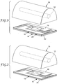
broadband radiation from a short pulse light source, preferably a flashlamp 12
as in Figure 1, is directed at a workpiece 14 to form a shaped image, such as a
three dimensional pattern 13, in the workpiece 14. A reflector 15 is placed
over the flashlamp 12 to guide the radiation, at a selected energy density,
toward the workpiece 14. A template 16, such as a mask 18 with a guide
shape, is positioned proximate the workpiece 14 to cast radiation onto the
workpiece 14 in the shape of the pattern 13.
Workpieces 14 of particular interest include a substrate (not shown).
One or more sides of the substrate may include a coating (not shown). If the
substrate does not include the coating, the substrate includes a boundary portion
(not shown) instead of the coating. The pattern 13 is preferably created in the
coating, if the substrate includes the coating, or in the boundary portion, if the
substrate does not include the coating.
The substrate may be made of many organic or inorganic materials,
including silicon, metal, composite materials that are impregnated with fibers
such as carbon and glass, or polymers, such as polyester, polycarbonate,
polyethylene, polyethylene terephthalate, polyamide, or polyimide. The
substrate may be flexible or rigid in structure. The boundary portion is
preferably made of the same material as the substrate. The coating includes a
surface coating layer and may include one or more additional coating layers.
The coating layers may be arranged in any desired order. The pattern 13 may
be formed in any of the coating layers, as desired, so long as the desired
coating layer is visible to a sufficient amount of radiation to form the pattern
13. Preferably, the coating layer in which the pattern 13 is formed is less than
about 1 µm thick.
Organic and inorganic materials may be included in the coating layers to
provide desired operative, structural, identifying, and aesthetic features. For
instance, one or more of the coating layers may be made of a conductive metal
to provide desired conductive characteristics. Examples of conductive metals of
interest include copper, silver, nickel, chromium, alloys of these, and indium
tin oxide. Also, one or more of the coating layers may be made of a magnetic
metal to provide desired magnetic characteristics. The magnetic metal, for
purposes of this disclosure, is an elemental metal or a metallic compound that
possesses magnetic properties. The magnetic metal may be the sole component
of a particular coating layer or may be a single component of several
components making up the particular coating layer, such as magnetic particles
distributed within the particular coating layer. Examples of magnetic metals
include iron, iron oxide, barium ferrite, cobalt nickel, cobalt phosphorous,
cobalt chrome, and oxides of cobalt.
Examples of potential workpieces include substrates coated with
magnetic metal or magnetic material, such as magnetic data storage disks,
sometimes referred to as floppy disks. Other examples of potential workpieces
include substrates coated with conductive metal, such as memory card circuits
and touch screen circuits. Additional examples of potential workpieces include
polymer-coated substrates, such as objects on which bar code information is
placed.
The short pulse light source, preferably the flashlamp 12, selectively
patterns the coating or boundary portion of the workpiece 14 by a well known
process called ablative decomposition, hereinafter referred to as ablation.
Ablative formation of the pattern 13 depends upon a substantial level of
absorption of short pulse width, high density energy in the coating or boundary
portion. Absorption of short pulse width, high density energy is known to
generate a substantial amount of heat in the coating or boundary portion in a
very short time period such that the generated heat stays in the coating or
boundary portion during the short time increments of the pattern ablation
process. The short pulse length, high density energy is believed to concentrate
in the coating or boundary portion proximate the pattern 13, rather than
bleeding into areas of the workpiece 14 away from the pattern 13 or into areas
of the workpiece 14 other than the coating or the boundary portion.
Favorable pattern ablation conditions include energy densities greater
than or equal to approximately 0.5 J/cm2 generated during a pulse width of less
than about one hundred microseconds (100 µsec). Lower density (less than
approximately 0.5 J/cm2), longer pulse width (greater than approximately 100
µsec) energy is not believed to fully concentrate in the coating or boundary
portion proximate the pattern 13, but instead is thought to cause undesirable
thermal effects in areas of the workpiece 14 located away from the pattern 13.
Preferably, the broadband radiation of the flashlamp 12 has high energy density
(greater than approximately 1.5 joules/centimeter2) that is achieved during a
short pulse width (less than about 100 µsec) to assure satisfactory ablative
imaging of the pattern 13 in the coating or the boundary portion of the
workpiece 14.
The range and distribution of the radiation wavelengths is also relevant
to selection of the light source, preferably the flashlamp 12. This wavelength
information is considered in combination with substrate and coating
characteristics, such as composition and thickness. Coatings and boundary
portions associated with different workpieces 14 absorb different wavelengths of
radiation at different rates, depending upon many variables, such as workpiece
14 composition, coating composition and thickness, and energy density of the
radiation. Since desirable ablation characteristics depend upon rapid absorption
of radiation energy, selection of radiation wavelengths which are quickly
absorbed by the coating or boundary portion of the workpiece 14 typically
improves pattern ablation. For example, it has been found that, for some
substrates and coatings, concentration of the radiation in the shorter
wavelengths, less than approximately 800 nm, improves ablation imaging and
economic and process efficiencies associated with ablation imaging.
Absorption of the radiation may be enhanced by application of
absorption enhancing agents. Absorption enhancing agents, for purposes of this
disclosure, are chemical agents that are applied to the coating or boundary
portion of the workpiece 14 for the purpose of enhancing absorption of
radiation, preferably select wavelengths of radiation, by the coating or the
boundary portion. Examples of absorption enhancing agents include certain
dyes and pigments. Another example of an absorption enhancing agent is an
oxide created in the surface of a metal coating. Such an oxide may offset the
reflective nature of certain metals such as aluminum.
The wavelength of the radiation contacting the coating or boundary
portion of the workpiece 14 may be varied to better match the wavelengths
absorbed by the coating or the boundary portion in several ways. For instance,
variation of power input to the flashlamp 12 typically varies the wavelength
distribution and the peak wavelength of the radiation. In another technique, an
optical filter (not shown) may be placed between the flashlamp 12 and the
workpiece 14 such that the radiation passes through the optical filter. The
optical filter may be configured to selectively screen undesired wavelength
components from the radiation. Screening of undesired wavelengths also
concentrates the energy density of the radiation in wavelengths of interest.
Screening of undesired wavelengths may optimize ablation of the pattern 13 by
reducing detrimental workpiece effects of the radiation such as heating of the
workpiece.
The substrate may also be selected or modified with absorbing dyes or
particles to reduce the intensity of energy reaching a coating on the backside of
the substrate. Alternatively, a reflective material can be used in the substrate
or as a sublayer to the backside coating to reduce the energy absorbed by the
backside coating or substrate.
In one embodiment, the flashlamp 12 is preferably a linear flashlamp.
The linear flashlamp is able to produce high power and energy density
discharges at shorter wavelengths in relatively short pulses on the order of 5
µsec. The linear flashlamp typically includes a quartz lamp tube with a wall
thickness of about 1 mm, an internal bore with a diameter in the range of about
3-20 mm, and a length of up to many centimeters. Electrodes, often made of
tungsten, are sealed into the ends of the lamp tube. Also, the lamp tube is
filled with a noble gas, preferably xenon for efficiency reasons.
The linear flashlamp is pulsed by quickly applying a high voltage,
typically in the range of 5-40 kv, to the electrodes using a capacitor bank. The
charge ionizes the xenon atoms to form a plasma that emits the radiation. The
high voltage is applied to the capacitor bank at a high rate, using a fast closing
dump switch to create a shortened pulse width on the order of 5 µsec. A flow
of low voltage direct current on the order of a few amps, known as a simmer
current, is preferably maintained through the electrodes, both during and
between pulses of the flashlamp 12, to keep the plasma warm. Warming of the
plasma prevents thermal shock within the flashlamp 12 when the flashlamp 12
is pulsed.
Additionally, the high density energy of the linear flashlamp is available
over a relatively large area, as compared to other radiation sources, such as
lasers. The large radiation coverage area coupled with the guide shape of the
mask 18 sometimes allows the light source, such as the flashlamp 12 to
desirably create multiple image features at a time without movement of the
flashlamp 12 relative to the mask 18 or the workpiece 14.
The large radiation coverage area of flashlamps, relative to the radiation
coverage area of lasers such as excimer lasers, minimizes undesirable regions
of damaged material in the coating or boundary portion that is ablated. As
already noted, each pulse of a laser creates a separate region of damaged
material. It is believed that the damaged material associated with the laser
results from diminished energy density in the coating or boundary portion
proximate the perimeter of the laser beam. It is thought that the diminished
energy density may be caused by beam divergence, beam jitter due to system
vibration, and beam jitter caused by non-uniform laser plasma generation.
The flashlamp 12 also creates a region of damaged material in the
coating or boundary portion during each pulse of the flashlamp. It is thought
that the damaged material associated with the flashlamp 12 is attributable to
diminished energy density in the coating or boundary portion proximate the
perimeter of the radiation emitted by the flashlamp 12. It is believed that the
diminished energy density associated with the flashlamp 12 may be due to
thermal diffusion proximate the perimeter of the pattern that is ablated. The
thermal diffusion apparently occurs due to absorption of radiation over a longer
period of time than observed for the laser. The slower absorption arises
because the energy density of the flashlamp is generated during a longer pulse
than that of the laser.
Though the flashlamp does create damaged material, the region of
damaged material of the flashlamp is less problematic than the region of
damaged material of the laser. The region of damaged material generated by
the laser is a significantly larger percentage of the area ablated than is the
region of damaged material associated with the flashlamp. Consequently,
ablation of the damaged material associated with the flashlamp requires less
corrective imaging than does ablation of the damaged material associated with
the laser. Consequently, the damaged material diminishes productivity of the
flashlamp at a significantly lower rate than for the laser.
In accordance with the present invention, the template 16, such as the
mask 18 with the guide shape, may be positioned proximate the coating or
boundary portion. The guide shape of the mask 18 comprises essentially one or
more shaped windows (not shown) which direct the radiation of the flashlamp
12 at the coating or boundary portion to form the pattern 13 in the workpiece
14. The workpiece 14 is located on one side of the mask 18, and the flashlamp
12 is located on the other side of the mask 12.
The mask 18 preferably includes underlying support for the window
portions of the mask 18. Supported masks avoid many alignment and mask
shape distortion problems. Also, supported masks are able to include isolated
areas of mask material, such as an X-Y pattern or the center of the letter "O".
Preferably, the mask 18 is made of a base material with high
transparency to the radiation of the flashlamp 12, such as fused silica,
commonly known as synthetic quartz. High transparency of the base material,
which spans the window areas of the mask, minimizes distortion and diffraction
of radiation passing through the mask and minimizes heating of the mask due to
absorption of radiation. The mask 18 also includes a surface coating that is
highly reflective to the radiation of the flashlamp 12. High mask 18 reflectivity
minimizes etching of the mask 18 in areas of the mask 18 where it is desired to
block the radiation and also minimizes undesirable heating of the mask 18.
In one embodiment, the surface coating of the mask 18 is made of
aluminum that is vacuum deposited on the fused silica base material to a depth
of approximately 600 nm. The aluminum is shaped to form the guide shape in
the mask 18 by standard semiconductor industry photolithographic and wet etch
processing techniques.
As an alternative to the mask 18, the template 16 may be an ink
formation (not shown) placed on or proximate the coating or boundary portion.
The ink formation is substituted for the mask 18. The ink formation serves as
a guide for the radiation of the flashlamp 12.
It has been found that the ink formation sometimes has voids that may
cause ablation of pinholes in the coating of the workpiece. When the laser,
such as the excimer laser, images the pattern in the workpiece through the ink
formation having voids, high resolution pinholes may be ablated in the coating
of the workpiece. However, when the flashlamp 12 images the pattern in the
workpiece through the ink formation that is substantially similar to the ink
formation used with the laser, a significant decrease in pinhole ablation has
been observed. Both the size and number of pinholes is diminished when the
flashlamp 12 ablates the pattern, as compared to when the laser ablates the
pattern. Minimizing the size and number of pinholes is desirable to reduce the
likelihood of opens in certain conductive patterns, such as the pattern 13 when
ablated in conductive metal.
It is believed that pinhole imaging decreases for the flashlamp, relative
to the laser, because of increased thermal effects in the coating that are
attributed to the flashlamp. Specifically, the energy density of the flashlamp 12
is applied to the coating during a longer time period than is the energy density
of the laser. Consequently, it is believed that thermal energy generated in the
coating by the flashlamp diffuses away from portions of the workpiece imaged
by flashlamp radiation that passes through voids in the ink formation. It is
thought that the decreased concentration of thermal energy in the workpiece
caused by diffusion of the energy in the workpiece decreases both the number
and size of pinholes imaged in the coating by the flashlamp. Other potential
explanations for diminished pinhole imaging associated with the flashlamp
include elevated radiation divergence of the flashlamp and decreased directional
uniformity of flashlamp rays.
In one embodiment, as in Figure 1, a buffer layer 20 is positioned
proximate the coating or boundary portion of the workpiece 14. It is known
that ablation of the pattern 13 in the coating or boundary portion leads to high
energy fragmentation of debris, and it is believed that the fragments of debris
travel on the order of one or two centimeters from the workpiece 14 absent the
buffer layer 20. The buffer layer 20 acts as a physical, impermeable barrier
that prevents movement of debris away from the workpiece 14, and thus
prevents debris from contacting the template 16, such as the mask 18.
The buffer layer 20 is located close enough to the coating or boundary
portion of the workpiece 14, it is believed, to prevent movement of debris more
than a few millimeters away from the workpiece 14. If the buffer layer 20
were not present, it is known that debris would contact and adhere to the mask
18 within the windows. Cleaning of the debris from the mask 18 or
replacement of the mask 18 would be needed to prevent dispersion and
diffraction of the radiation and undesirable imaging effects. Debris cleaning is
disruptive and mask 18 replacement is expensive.
When used with the ink formation, the buffer layer 20 acts as a
physical, impermeable barrier that prevents movement of the debris away from
the workpiece 14, and thus prevents debris from contacting the flashlamp 12.
The ink formation is positioned between the buffer layer 20 and the workpiece
14 if the ink formation is applied directly to the coating or boundary portion.
Otherwise, the buffer layer 20 is positioned between the ink formation and the
workpiece 14. If the buffer layer 20 were not present, it is known that debris
would contact and adhere to the flashlamp 12. Cleaning of debris from the
flashlamp 12 or replacement of the flashlamp 12 would be needed to prevent
dispersion and diffraction of the radiation and undesirable imaging effects.
Debris cleaning is disruptive to production, and flashlamp 12 replacement is
expensive.
In one embodiment, as in Figure 2, the substrate of the workpiece 14 is
the buffer layer 20. A coated side (not shown) of the substrate includes the
coating. The substrate also includes a non-coated side (not shown). The coated
and non-coated sides oppose each other. The flashlamp 12 is located on the
non-coated side of the substrate. The radiation of the flashlamp 12 enters the
non-coated side of the substrate and passes through the substrate. The radiation
contacts the coating on a side of the coating that is in contact with the substrate
and creates the pattern 13 in the coating of the workpiece 14.
In more preferred embodiments, the buffer layer 20 is either a sheet of
film 22, as in Figure 1, or a web of film (not shown) positioned to isolate the
coating or boundary portion from the flashlamp 12. All comments about the
buffer layer 20 apply to the sheet of film 22, the web of film, and the substrate
(when the substrate is the buffer layer 20), unless otherwise indicated. The
buffer layer 20 is durable enough to provide adequate handling characteristics
and strong enough to prevent passage of debris liberated from the workpiece
14.
It is generally desirable to place the buffer layer 20 proximate the
coating or the boundary portion such that the flashlamp 12 may be placed close
to the workpiece 14. Close spacing of the flashlamp 12 to the workpiece 14
may produce more favorable imaging economics and improved pattern
characteristics. Close spacing also limits contamination of non-imaged portions
of the workpiece 14 located outside the pattern 13.
However, the degree of close contact desired between the buffer layer
20 and the coating or the boundary portion may depend upon workpiece
variables, such as the roughness of the coating or the boundary portion of the
workpiece 14. For example, some coatings have rougher surfaces than other
coatings. It is believed that if the buffer layer 20 is in intimate contact with a
rough surface such that the buffer layer 20 conforms to the rough surface, the
pattern 13 created by the radiation will likely have somewhat poorer resolution.
It is believed that the poorer resolution will arise due to dispersion and
diffraction effects created when the radiation passes through the buffer layer 20
at other than a substantially perpendicular orientation, relative to the buffer
layer 20.
Close spacing of the buffer layer 20 and the coating is inherently present
when the substrate is the buffer layer 20. Otherwise, referring to Figure 1,
close spacing of the buffer layer 20 and the coating or the boundary portion
may be obtained by laying the buffer layer 20 against the coating or the
boundary portion of the workpiece 14 such that the buffer layer 20 and the
workpiece 14 are in fixed contact with each other. Also, the buffer layer 20,
such as the sheet of film, may be laminated or extruded onto the coating or the
boundary portion using conventional lamination or extrusion techniques and
equipment.
In another alternative, the coating or boundary portion and the buffer
layer 20 may be placed in dynamic relationship using a continuous staging
system such that the buffer layer 20 and the coating or the boundary portion
each move at the same speed and in the same direction and are in contact with
each other, but are not fixed to each other. Here, the workpiece 14 takes the
form of a workpiece web (not shown) and the buffer layer 20 takes the form of
a buffer web (not shown).
The buffer layer 20 is preferably selected to assure optimum image
shaping in the coating or the boundary portion of the workpiece 14 and efficient
use of the radiation. The radiation desired at the coating or the boundary
portion to create the pattern 13 depends heavily on the absorption characteristics
of the coating or the boundary portion of the workpiece 14. The radiation
actually reaching the coating or the boundary portion depends on the
transmittance of the radiation through the buffer layer 20. A higher
transmittance through the buffer layer 20 decreases the energy requirements of
the flashlamp 12 and decreases absorptive heating of the buffer layer 20. The
transmittance of the buffer layer 20 is highly dependant upon the material the
buffer layer 20 is made of and the thickness of the buffer layer 20.
The buffer layer 20 is sufficiently transparent to the radiation of the
flashlamp 12 such that the radiation, after passing through the buffer layer 20,
has sufficient remaining energy to form the pattern 13 in the coating or the
boundary portion of the workpiece 14. The buffer layer 20 is preferably highly
transparent to the radiation such that the flashlamp 12 efficiently develops the
pattern 13 in the coating or the boundary portion. Preferably, the buffer layer
20 is sufficiently transparent to the radiation to allow at least about fifty percent
(50%), and more preferably at least about eighty percent (80%), of the
radiation to pass through the buffer layer 20.
The buffer layer 20 is also selected to assure optimum image shaping in
the coating or the boundary portion. Image shaping depends on the geometric
changes in the radiation, such as scattering and diffraction of the radiation, due
to passage of the radiation through the buffer layer 20. The geometric changes
in the radiation are created by manufacturing defects, such as extrusion lines,
surface irregularities, and caliper non-uniformity. Preferably, the buffer layer
20 has minimal manufacturing defects and is of sufficient quality to produce
good image resolution in the coating or the boundary portion.
The transmittance of the buffer layer 20 and the geometric changes
imposed upon the radiation depend upon the material the buffer layer 20 is
made of, the thickness of the buffer layer 20, and manufacturing defects present
in the buffer layer 16. It has been discovered that some organic polymer films,
such as particular grades of polypropylene film, are particularly conducive to
optimum image shaping and efficient use of radiation from the flashlamp 12,
under certain circumstances.
The buffer layer 16, preferably the sheet of film, may be made of a
commercial grade of polymer film, such as commercial grade polypropylene
and commercial grade polyethylene. However, commercial grades of polymer
film are not the film of choice because commercial grades of polymer film
typically have manufacturing defects, such as extrusion lines, surface
irregularities and caliper non-uniformity. These defects typically introduce
irregularities into the radiation as the radiation passes through the sheet of film.
Additionally, commercial grades of polymer films with these defects tend to
absorb energy from the radiation. This causes the film to heat up and may
decrease the durability and useful life of the polymer film.
If commercial grade polymers are nonetheless selected, it has been
found that commercial grade polyethylene, relative to commercial grade
polypropylene, is significantly less transparent to some wavelength bands of
interest. Correspondingly, the power supplied to the flashlamp 12 for creating
an identical pattern in an identical workpiece 14 is increased for a particular
flashlamp 12 emitting radiation through commercial grade polyethylene film as
compared to a similar flashlamp 12 emitting radiation through commercial
grade polypropylene film.
Preferably, the buffer layer 20 is made of capacitor grade biaxially-oriented
polypropylene (BOPP). It has been found that capacitor grade
polypropylene provides a high transmittance to radiation of the flashlamp 12.
Additionally, the capacitor grade polypropylene has a smooth finish, uniform
thickness, and minimal surface imperfections, such as casting marks. These
qualities minimize changes in radiation geometry as the radiation passes through
the sheet of film, thereby preserving pattern resolution and extending film life.
After the pattern 13 is created in the coating or boundary portion, the
buffer layer 20 is removed from the workpiece 14. Significant amounts of
debris are typically removed with the sheet of film when the buffer layer 20 is
made of biaxially-oriented polypropylene film. The coating or boundary
portion is then cleaned of remaining debris using a conventional carbon dioxide
snow blasting process. According to the snow blasting process, carbon dioxide
at approximately 850 PSI (59.76 kg/cm2) is mixed with ambient air to produce
crystallized snow granules. The crystallized snow granules are projected at the
coating or the boundary portion of the workpiece 14 in "sand blast" fashion
using a commercially available blasting gun.
Although many embodiments may be practiced in accordance with this
invention, the invention is demonstrated by the following illustrative but
nonlimiting examples.
EXAMPLES
Examples 1-2 (Flashlamp Ablation of A Metal-Coated Substrate)
The workpiece 14 of each example, referring to Figure 1, was a vacuum
metalized polymer film made by evaporating a 75 nm coating of copper onto a
polyethylene terephthalate (PET) substrate using a standard E-beam evaporation
technique within a vacuum chamber. The buffer layer 20 was made of
capacitor grade biaxially oriented polypropylene film available from Bollmet
Inc., of Dayville, Connecticut. The buffer layer 20 was 0.001 inches (25 µm)
thick.
The flashlamp 12 was a Part No. ILCT-18 linear flashlamp available
from ILC Technology, Inc. of Sunnyvale, California. The flashlamp 12
included a transparent fused silica tube with a wall thickness of 1.0 mm and a
6.0 mm diameter bore. The bore contained pressurized xenon at a gauge
pressure of 400 mm of Hg (0°C). The flashlamp 12 had a pulse width of 6
µseconds (FWHM) with input energy of 100 joules. A charging voltage of
about 10 kv was applied to a capacitor with about 2 µF of capacitance to pulse
the flashlamp 12. A simmer current of about 1.7 amps was applied to the
electrodes of the flashlamp 12 to keep the plasma warm and prevent thermal
shock to the flashlamp 12. Radiation from the flashlamp 12 was directed by
the reflector 15, which was elliptically shaped, toward a portion of the
workpiece 14 with an area of about 44.5 cm2. The reflector aperture was 5.0
cm wide and the flashlamp arc was 8.9 cm long.
Example 1
The ink formation was printed on the copper coating of the workpiece
14 by a conventional technique prior to flashlamp 12 exposure. The pattern 13
was a series of about 30 parallel rows of lines. Each row of lines included
lines ranging in width from 0.002 inches (50 µm) to 0.010 inches (250 µm).
The buffer layer 20 was placed over the ink formation in close contact with the
ink formation and the copper coating. An area of about 14 cm2 of the targeted
44.5 cm2 area was ablated when the flashlamp was pulsed. This 14 cm2 area
included good resolution for lines as small as 0.004 inches (100 µm) wide with
0.002 inch (50 µm) line-to-line spacing. Additionally, the buffer layer 20
prevented ablation debris from dirtying the flashlamp 12 and the reflector 15.
Example 2
The buffer layer 20 was placed over the workpiece 14 in close contact
with the copper coating. The mask 18 with the guide shape was placed in close
contact with the buffer layer 20. The base material of the mask 18 was made
of fused silica and the surface coating material was aluminum. The aluminum
was vacuum deposited on the fused silica base material to a depth of
approximately 600 nm. The aluminum was shaped to form the guide shape in
the mask 18 by standard semiconductor industry photolithographic and wet etch
processing techniques.
The pattern 13 was a series of about 30 parallel rows of lines. Each
row of lines included lines ranging in width from 0.002 inches (50 µm) to
0.010 inches (250 µm). An area of about 14 cm2 of the targeted 44.5 cm2 area
was ablated. This 14 cm2 area included good resolution for lines as small as
0.006 inches (150 µm) wide with 0.003 inch (75 µm) line to line spacing.
Also, the buffer layer 20 prevented ablation debris from contacting and dirtying
the mask 18, the flashlamp 12, and the reflector 15.
Example 3
The workpiece 14 of this example was substantially the workpiece
described for Examples 1 and 2. The template 16 was the ink formation
formed of a conventional organic ink and printed on the copper coating of the
workpiece 14 by a conventional technique. The guide pattern of the ink
formation included 0.004 inch (100 µm) wide lines with 0.008 inch (200 µm)
center to center spacing. The buffer layer 20 was made of capacitor grade
biaxially oriented polypropylene film available from Bollmet Inc., of Dayville,
Connecticut. The buffer layer 20 was 0.001 inches (25 µm) thick.
The flashlamp 12 was a Model No. L786E linear flashlamp available
from ILC Technology, Inc. of Sunnyvale, California. The flashlamp 12
included a transparent fused silica tube with a wall thickness of 1.0 mm and a
8.0 mm diameter bore. The bore contained pressurized xenon at a gauge
pressure of 400 mm of Hg (0°C). The flashlamp 12 had a pulse width of 4
µseconds (FWHM) with input energy of 200 joules and ablated about 60 square
centimeters per pulse.
A charging voltage of about 21.8 kv was applied to a capacitor with
about 0.84 µF of capacitance to pulse the flashlamp 12. A simmer current of
about 1.9 amps was applied to the electrodes of the flashlamp 12. Radiation
from the flashlamp 12 was directed by the reflector 15, which had a cusp
shape, toward a portion of the workpiece 14. The reflector aperture was 5.0
cm wide and the flashlamp arc was 20.3 cm long. The flashlamp 12 produced
an energy density of 1.5 J/cm2 at the workpiece 14.
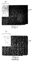
(In Figures 3 and 5, light colored areas are areas where coating was
ablated, and dark colored areas are areas where coating was not ablated).
(Also, Figure 3 is magnified about 12.5 times and Figure 5 is magnified about
200 times).
The flashlamp 12 generated a pattern of lines 23 in the workpiece 14 as
in Figure 3. The flashlamp 12 ablated the pattern of lines 23 with acceptable,
reduced resolution, as compared to the laser of Comparison Example 1. It is
believed that lower energy density per unit time associated with the flashlamp
12 was responsible for the reduced resolution.
Each pulse of the flashlamp 12 also created the narrow region (not
shown) of damaged material in the coating. The area of damaged material
created by each pulse of the laser of Comparison Example 1, as a percentage of
the coating ablated, was several times larger than that created by each pulse of
the flashlamp 12.
Comparison Example 1
The workpiece 14, template 16, and buffer layer 20 of this example
were substantially the same as the workpiece 14, template 16, and buffer layer
20 of Example 3. A laser (not shown) was substituted in place of the flashlamp
12 and the reflector 15.
The laser was a Model LPX 315 150 Watt Excimer laser available from
Lambda Physik of Acton, Massachusetts. The Model LPX 315 laser was
capable of selective beam energy output ranging from 400 to 800 mJ at up to a
150 Hz pulse rate. The laser had a pulse width of 0.02 microseconds (FWHM)
and ablated in the range of 2 to 3 square centimeters per pulse. The excimer
Laser was optimized for fluorine and produced ultraviolet radiation with a wave
length of 248 nm. A cylindrical converging lens with a 42 inch (106.68 cm)
focal length and a cylindrical diverging lens with a 6 inch (15.24 cm) focal
length were arranged to focus and shape the beam of the laser. The distances
between the converging lens and the laser and between the converging lens and
the diverging lens were adjusted to provide the combination of beam width,
height, and energy density required for ablation of the copper coating.
The workpiece 14 was mounted on an X-Y translation stage that was
translated through the laser beam to scan the guide shape of the ink formation
to create the pattern in the copper coating. The X-Y translation stage was
translated in the Y direction at a linear rate of 100 inches/min (254 cm/min).
The laser produced an energy density of 125 mJ/cm2 at the workpiece 14. The
energy density was measured by an apertured Model ED-500 Joulemeter
available from Gentech of Ste-Fog, Quebec, Canada. The meter was placed the
same distance from the laser as existed between the laser and the workpiece 14.
(In Figures 4 and 6, light colored areas are areas where coating was
ablated, and dark colored areas are areas where coating was not ablated).
(Also, Figure 4 is magnified about 12.5 times and Figure 6 is magnified about
200 times).
The laser generated a pattern of lines 25 in the workpiece 14 as in
Figure 4. The laser ablated the pattern of lines 25 with good resolution and
also ablated pinholes 26 where the ink formation covered the workpiece 14.
The pinholes 26, as compared to the pinholes 24 ablated by the flashlamp 12 in
Example 3, are significantly larger in size and greater in number. The pinholes
26 in the metal coating, more clearly shown in Figure 6, are more likely to
create a circuit path open than are the pinholes 24 formed by the flashlamp 12
due to the larger size and increased number of the pinholes 26 relative to the
pinholes 24.
During each pulse, the laser created the narrow region (not shown) of
damaged material in the coating proximate the coating that was ablated. The
area of damaged material created per pulse of the laser, as a percentage of the
coating ablated, was several times larger than that created by each pulse of the
flashlamp 12 in Example 3.