EP0658047A1 - Automatic adapting image sensing and display system - Google Patents
Automatic adapting image sensing and display system Download PDFInfo
- Publication number
- EP0658047A1 EP0658047A1 EP94119604A EP94119604A EP0658047A1 EP 0658047 A1 EP0658047 A1 EP 0658047A1 EP 94119604 A EP94119604 A EP 94119604A EP 94119604 A EP94119604 A EP 94119604A EP 0658047 A1 EP0658047 A1 EP 0658047A1
- Authority
- EP
- European Patent Office
- Prior art keywords
- sweeping
- image
- circuit
- signal
- vertical
- Prior art date
- Legal status (The legal status is an assumption and is not a legal conclusion. Google has not performed a legal analysis and makes no representation as to the accuracy of the status listed.)
- Granted
Links
Images


Classifications
-
- H—ELECTRICITY
- H04—ELECTRIC COMMUNICATION TECHNIQUE
- H04N—PICTORIAL COMMUNICATION, e.g. TELEVISION
- H04N3/00—Scanning details of television systems; Combination thereof with generation of supply voltages
- H04N3/10—Scanning details of television systems; Combination thereof with generation of supply voltages by means not exclusively optical-mechanical
- H04N3/16—Scanning details of television systems; Combination thereof with generation of supply voltages by means not exclusively optical-mechanical by deflecting electron beam in cathode-ray tube, e.g. scanning corrections
- H04N3/27—Circuits special to multi-standard receivers
-
- H—ELECTRICITY
- H04—ELECTRIC COMMUNICATION TECHNIQUE
- H04N—PICTORIAL COMMUNICATION, e.g. TELEVISION
- H04N25/00—Circuitry of solid-state image sensors [SSIS]; Control thereof
Definitions
- the invention relates to an image sensor and display device, and more particularly to an image sensor and display device available to various size pixels of image sensors by compensation of image stress of image signals and subsequent display.
- the image sensor has a plurality of unit pixels aligned in matrix within an active image area having a predetermined screen ratio.
- Each of the unit pixels performs a photo-electric conversion to generate image signals for sequential reading out operations and subsequent transfer thereof to the display device with a predetermined screen ratio.
- the screen ratio of a vertical length to a horizontal length of the active image area is 3 : 4 in the NTSC and PAL regulations, while in the high definition television system the screen ratio is 9 : 16.
- the optical image informations are converted to the image signals by the image sensor with a predetermined vertical-to-horizontal ratio of the active image area on which the pixels are aligned in matrix.
- the image signals are transferred to the display device for display on various sizes of the regulated screens as described above.
- the display screen comprises an active image area having a vertical-to-horizontal ratio of 9 : 16 and having scanning line numbers of 1036 in which the scanning lines run in the horizontal direction as illustrated in FIG. 1.
- the one time scanning on all the scanning lines are carried out in a time of 1/30 seconds for the two-dimensional display.
- the screen comprises an interlace scanning of A and B fields.
- the active image are defined by a vertical scanning period and a horizontal scanning period.
- Inactive area outside the active image area but on the screen comprises a L-shaped area defined by a vertical retrace line period of 89 scanning lines and a horizontal retrace line period as illustrated in FIG. 1.
- the active image area has a vertical size of 7.9 mm and a horizontal size of 14.0 mm for the alignment of the plurality of unit pixels.
- 2,000,000 pixels are aligned in such a matrix that 1036 pixels are aligned in the vertical direction and 1920 pixels are aligned in the horizontal direction wherein each pixel has a size of 7.6 X 7.3 micrometers.
- 1035 pixels are aligned in the vertical direction and 1258 pixels are aligned in the horizontal direction wherein each pixel has a size of 7.61 X 13.56 micrometers.
- each pixel is rectangular-shaped, but not square-shaped.
- each pixel is rectangular-shaped, but not square-shaped.
- 250,000 pixels, 330,000 pixels and 380,000 pixels are used wherein unit pixels have the same vertical size but various horizontal sizes to improve a horizontal resolution.
- the unit pixel is square-shaped.
- the reading out operation for the image signals from the image sensors is carried out.
- 2,000,000 pixels requires 4.25 MHz and 1,300,000 pixels requires 48.6MHz.
- a single scanning line on the screen is continued to be scanned for 29.6 microseconds.
- the active image area on the display screen includes 1035 or 1036 scanning lines.
- the image in the active image area of the solid state image sensor is displayed without any lack of the image.
- a variation of the frequency for the reading put operation may merely be represented as a variation of the horizontal resolution on the screen.
- FIG. 2 illustrates configurations of an image camera 1 and a display device 5.
- the image camera 1 is provided with a camera lens 2.
- the image camera 1 includes a solid state image sensor 3, a driving circuit 41 being connected to the solid state image sensor 3 for driving the sold state image sensor 3 and an image signal processor 42 being connected to the solid state image sensor 3 for processing the image signals into which the optical images are converted by the solid state image sensor 3.
- the image signal processed by the image signal processor is outputted from an output terminal to be inputted into in input terminal of the display device 5.
- the display device 5 includes a screen section 6 with a cathode ray tube, a horizontal scanning circuit for permitting a horizontal scanning of electron beam on the screen section and a vertical scanning circuit for permitting a vertical scanning of electron beam on the screen section as well as an image signal display circuit for permitting an image signal display on the screen.
- image signals corresponding to 1125 scanning limes on the screen or 1045 to 1036 scanning lines on the active image area are red out by the solid state image sensor 3 in cooperation with the driving circuit 41 for processing of the image signals and subsequent output from the output terminal of the image camera 1. Thereafter, the image signals are inputted into the input terminal of the display device 5 to be supplied through the display circuit 81 to the screen on which all image informations picked put in the active image area of the solid state image sensor 3 are surely displayed.
- the enlargement and reduction of the image are used.
- An improvement in the resolution by the interpolation between the pixels in the digital processing and a color tone compensation are also required.
- the squired pixels of the solid state image sensor are suitable.
- a high definition image is essential. At present, a one dimensional high definition image input scanner has been realized.
- the high definition television system image sensor with the rectangular-shaped pixels picks up the image for computer processing.
- the image signals are required to be converted into analog signals for sampling at a predetermined frequency and subsequent conversion of digital signals for the squared pixels.
- This analog to digital signal conversion may result in a deterioration of signal-to-noise ratio.
- Beat with the sampling frequency may permit a periodic noise generation.
- An expensive high speed analog-to-digital converter is required thereby resulting in an increase of the cost of the device.
- a firs way is to keep the number of scanning lines but vary the number of pixels aligned in the horizontal direction.
- unit pixels are designed to have the squared definition of 7.3 micrometers and 7.3 micrometers while normally the vertical and horizontal sizes of the unit pixels are 7.6 micrometers and 7.3 micrometers respectively in use for the high definition television system.
- a second way is to design the squared unit pixels to have a size of 7.3 micrometers X 7.3 micrometers so that the number of the active squared pixels is increased from 1036 up to 1080.
- 1080 X 1920 pixels are aligned in the active image area. Notwithstanding, the number of the pixels aligned in the horizontal direction is not changed. Hence, the reading out frequency for the image signal is the same as that of the 2,000,000 pixels.
- a vertical sweeping time is compensated to be extended by 4% so that 1080 scanning lines may be displayed on the screen thereby as illustrated in FIG. 3, the image picked up by the image sensor with the squared pixels may be completely displayed on the high definition television screen of 9 : 16 without any lack of the image or any image distortion. Notwithstanding, this way requires a judgment of whether the image signals are picked up by the rectangular-shaped pixels of the high definition television image sensor or by the squared pixels image sensor and subsequent switching operations of the vertical sweeping voltage and the sweeping time. Actually, it is difficult to judge whether the image displayed on the screen has the 4% image distortion. In the above viewpoints, it has been required to develop a novel display device.
- the invention provides a novel image camera including an image sensor for conversion into image signals and a processor being connected to the image sensor for fetching the image signals and subsequent processing the image signals to superimpose recognition signals, that indicate a kind of the image sensors, on a part of a retrace line period of the image signals.
- the invention also provides a novel display device including a monitor screen, a detector for detecting the recognition signals superimposed on the part of the retrace line period of the image signals and a control section for controlling vertical and horizontal sweeping speeds on a monitor screen of the display device.
- the invention also provides a novel image sensing and displaying system including an image camera and a display device being connected to receive image signals and other informations from the image camera, wherein the camera includes an image sensor for conversion into image signals and a processor being connected to the image sensor for fetching the image signals and subsequent processing the image signals to superimpose recognition signals, that indicate a kind of the image sensors, on a part of a retrace line period of the image signals, and also wherein the display device includes a monitor screen, a detector for detecting the recognition signals superimposed on the part of the retrace line period of the image signals and a control section for controlling vertical and horizontal sweeping speeds on a monitor screen of the display device.
- FIG. 1 is a view illustrative of the screen for the high definition television.
- FIG. 2 is a diagram illustrative of the conventional configurations of the image camera and the display device.
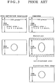
- FIG. 3 is a view illustrative of various images displayed on screens with or without image distortion.
- FIG. 4 is a diagram illustrative of a novel configuration of an image camera and a display device in a first embodiment according to the present invention.
- FIG. 5 is a diagram illustrative of vertical sweep wave-forms used in a first embodiment according to the present invention.
- FIGS. 6A and 6B are diagrams illustrative of superimposition of recognition signals on a part of a retrace line period in a first embodiment according to the present invention.
- FIG. 7 is a diagram illustrative of a novel configuration of an image camera and a display device in a second embodiment according to the present invention.
- a novel image sensing and displaying system includes an image camera and a display device being connected to receive image signals and other informations from the image camera.
- the camera includes an image sensor for conversion into image signals and a processor being connected to the image sensor for fetching the image signals and subsequent processing the image signals to superimpose recognition signals, that indicate a kind of the image sensors, on a part of a retrace line period of the image signals.
- the display device includes a monitor screen, a detector for detecting the recognition signals superimposed on the part of the retrace line period of the image signals and a control section for controlling vertical and horizontal sweeping speeds on a monitor screen of the display device.
- the image sensor may comprise 2,000,000 squared pixels comprising solid state image sensors aligned in matrix on an active image area so that 1080 pixels are aligned in the vertical direction and 1920 pixels are aligned in the horizontal direction.
- the active image area has a vertical-to-horizontal size ratio of 9 : 16.
- the image sensor is driven at a reading out frequency of 74.25 MHz.
- the image camera is provided with a recognition pulse superimposition circuit so that an output signal has a vertical retrace line period which predetermined position is superimposed with a recognition pulse indicating that the image was picked up by the squared pixel image camera.
- the display device may be designed for a high definition television display and being provided with a recognition pulse detection circuit and a sweeping control circuit.
- the recognition pulse detecting circuit may detect any recognition pulse signal so either that a vertical sweeping speed is reduced by 4% or that a sweeping time is extended by 4% to thereby permit 1080 active scanning lines to be displayed on the screen, resulting in distortion-free image being displayed on the screen.
- FIG. 4 A first embodiment according to the present invention will be described in detail with reference to FIG. 4 in which an image sensing and displaying system is provided.
- the image sensing and displaying system comprises an image camera 1 and a display device 5.
- the image camera is provided with a camera lens 2.
- the image camera 1 includes a solid state image sensor 3, a driving circuit 41 being connected to the solid state image sensor 3 for driving the solid state image sensor 3, an image signal processing unit 42 being connected to the solid state image sensor 3 for receipt of the image signals from the solid stet image sensor 3 and subsequent processing of the image signals and a recognition pulse signal superimposition circuit 43 being connected to the image signal processing unit 42 for receipt of the image signal from the mag signal processing unit 42 and subsequent superimposition of an recognition pulse signal on a predetermined position in a vertical retrace line period of the image signal.
- the recognition pulse signal is to indicate a kind of the image camera with specific pixels. In this embodiment, the squared pixels are sued.
- the image signal superimposed with the recognition pulse signal is outputted from an output terminal of the image camera 1.
- the output terminal of the image camera 1 is connected to an input terminal of the display device 5 so that the input terminal may receive the image signals super
- the display device 5 has a screen section 6 comprising a cathode ray tube.
- the display device 5 includes a horizontal sweeping circuit 71 being connected to the screen section 6 with the cathode ray tube for conducting a sweeping of an electron beam in the horizontal direction on the cathode ray tube of the screen section 6.
- the display device 5 includes a vertical sweeping circuit 72 being connected to the screen section 6 with the cathode ray tube for conducting a sweeping of an electron beam in the vertical direction on the cathode ray tube of the screen section 6.
- the display device 5 includes an image signal display circuit 81 being connected to the screen section 6 with the cathode ray tube for permitting the image to be displayed on the screen 6.
- the display device 5 also includes a recognition pulse signal detecting circuit 82 being connected to the input terminal for receipt of the image signals superimposed with the recognition pulse signal in order to detect the recognition pulse signal.
- the recognition pulse signal detecting circuit 82 is connected to the image signal display circuit 81 for transmitting the image signals without the detected recognition pulse signal into the image signal display circuit 81, which the recognition pulse signal detecting circuit 82 is further connected to a vertical sweeping control circuit 83 to supply the detected recognition pulse signal only into the vertical sweeping control circuit 83 being connected to the vertical sweeping circuit 72 so that the vertical sweeping control circuit 83 controls, according to the recognition pulse signal, a sweeping speed and a sweeping time in the vertical direction.
- the image camera 1 of this embodiment according to the present invention has a structural difference from the prior art in providing the recognition pulse signal superimposition circuit 43.
- the display device 5 of this embodiment according to the present invention has a structural difference from the prior art in providing the recognition pulse signal detecting circuit 82 and the vertical sweeping control circuit 83.
- FIG. 5 illustrates vertical sweeping voltage waveforms of the invention and the normal high definition television system.
- the vertical sweeping voltage waveform of the invention has an extended sweeping period and a reduced retracing line period as compared to the normal high definition television regulation.
- FIGS. 6A and 6B illustrate pulse signal waveforms for the normal high definition television system and the novel system in the vertical retracing line period and in the vertical scanning period.
- the vertical retracing line period includes 45 scanning lines and 45 corresponding synchronous pulse signals.
- the image signals are superimposed on or after a forty sixth scanning line 46H in the vertical scanning period.
- the synchronous pulse signals are for counting of a timing for feeding the image signals but never include any image signal.
- the recognition pulse signal is superimposed on the synchronous pulse signal before the vertical scanning period. In this embodiment, the recognition pulse signal is superimposed on a forty third pulse 43H or on a third pulse before the vertical scanning period.
- the superimposition of the recognition pulse signal on the pulse signal before the vertical scanning period may provide no affection to the image signals in the vertical scanning period. It is available to superimpose the recognition pulse signal on a pulse signal in the vertical retracing line period before the vertical scanning period to make the image signals free from any affection by the superimposition of the recognition pulse signal that indicates a kind of the pixels involved in the image camera.
- the recognition pulse signal may comprise a low level corresponding to the black in a first half period of the forty third pulse 43H and a high level corresponding to the white in a second half period of the forty third pulse 43H. Such a single pulse waveform is sufficient for constituting the recognition pulse signal that indicates a kind of the image camera.
- the recognition pulse signal As modifications for superimposition of the recognition pulse signal, it is available to superimpose the recognition pulse signals for every time periods, for example, at one second interval or five seconds interval. It is also available to superimpose the recognition signal on a horizontal retracing line period to avoid the scanning period including the image signals.
- the recognition pulse signal detection circuit 82 detects any recognition signal on the forty third pulse 43H.
- the recognition pulse signal indicates that the image camera includes the squared pixels as the solid state image sensors.
- the recognition pulse signal detection circuit 82 detects no recognition pulse signal on the forty third pulse 43H in the vertical retrace line period, then the display of the image is carried out according to the normal high definition television regulation.
- the vertical sweep control circuit controls the vertical sweep circuit 72 so that the vertical sweeping speed is reduced by 4% and the vertical sweeping time is extended by 4% thereby the number of the active scanning lines is increased from 1036 to 1080, resulting in a perfection of the image display on an entire of the 9 : 16 ratio screen for the high definition television.
- the number of the displayed scanning lines is increased by 44.
- 45 scanning lines are ensured to prevent any problem in displaying the image on the 9 : 16 high definition television screen.
- the novel system may render the solid state image sensor and the display device commonly usable or compatible between the computer systems and the high definition television systems.
- FIG. 4 A second embodiment according to the present invention will be described in detail with reference to FIG. 4 in which an image sensing and displaying system is provided.
- the image sensing and displaying system comprises an image camera 1 and a display device 5.
- the image camera is provided with a camera lens 2.
- the image camera 1 includes a solid state image sensor 3, a driving circuit 41 being connected to the solid state image sensor 3 for driving the solid state image sensor 3, an image signal processing unit 42 being connected to the solid state image sensor 3 for receipt of the image signals from the solid stet image sensor 3 and subsequent processing of the image signals and a recognition pulse signal superimposition circuit 43 being connected to the image signal processing unit 42 for receipt of the image signal from the mag signal processing unit 42 and subsequent superimposition of an recognition pulse signal on a predetermined position in a horizontal retrace line period of the image signal.
- the recognition pulse signal is to indicate a kind of the image camera with specific pixels. In this embodiment, the squared pixels are sued.
- the image signal superimposed with the recognition pulse signal is outputted from an output terminal of the image camera 1.
- the output terminal of the image camera 1 is connected to an input terminal of the display device 5 so that the input terminal may receive the image signals super
- the display device 5 has a screen section 6 comprising a cathode ray tube.
- the display device 5 includes a horizontal sweeping circuit 71 being connected to the screen section 6 with the cathode ray tube for conducting a sweeping of an electron beam in the horizontal direction on the cathode ray tube of the screen section 6.
- the display device 5 includes a vertical sweeping circuit 72 being connected to the screen section 6 with the cathode ray tube for conducting a sweeping of an electron beam in the vertical direction on the cathode ray tube of the screen section 6.
- the display device 5 includes an image signal display circuit 81 being connected to the screen section 6 with the cathode ray tube for permitting the image to be displayed on the screen 6.
- the display device 5 also includes a recognition pulse signal detecting circuit 82 being connected to the input terminal for receipt of the image signals superimposed with the recognition pulse signal in order to detect the recognition pulse signal.
- the recognition pulse signal detecting circuit 82 is connected to the image signal display circuit 81 for transmitting the image signals without the detected recognition pulse signal into the image signal display circuit 81, which the recognition pulse signal detecting circuit 82 is further connected to a horizontal sweeping control circuit 85 to supply the detected recognition pulse signal only into the horizontal sweeping control circuit 85 being connected to the horizontal sweeping circuit 71 so that the horizontal sweeping control circuit 85 controls, according to the recognition pulse signal, a sweeping speed and a sweeping time in the horizontal direction.
- the image camera 1 of this embodiment according to the present invention has a structural difference from the prior art in providing the recognition pulse signal superimposition circuit 43.
- the display device 5 of this embodiment according to the present invention has a structural difference from the prior art in providing the recognition pulse signal detecting circuit 82 and the vertical sweeping control circuit 85.
- the horizontal sweeping voltage waveform of the invention has an extended sweeping period and a reduced retracing line period as compared to the normal high definition television regulation.
- the recognition pulse signal is superimposed on the synchronous pulse signal before the horizontal scanning period.
- the recognition pulse signal is superimposed before the horizontal scanning period. Since any pulse signal includes no image signal, the superimposition of the recognition pulse signal on the pulse signal before the horizontal scanning period may provide no affection to the image signals in the horizontal scanning period. For that reason, it is available to superimpose the recognition pulse signal on a pulse signal in the horizontal retracing line period before the horizontal scanning period to make the image signals free from any affection by the superimposition of the recognition pulse signal that indicates a kind of the pixels involved in the image camera.
- the recognition pulse signal detection circuit 82 detects any recognition signal indicating that the image camera 1 includes the squared pixels as the solid state image sensors. When the recognition pulse signal detection circuit 82 detects no recognition pulse signal on the horizontal retrace line period, then the display of the image is carried out according to the normal high definition television regulation. By contrast, if the recognition pulse signal detection circuit 82 detects the recognition pulse signal on the horizontal retrace line period, then the horizontal sweep control circuit controls the horizontal sweep circuit 72 so that the horizontal sweeping speed is reduced by 4% and the horizontal sweeping time is extended by 4% thereby the number of the active scanning lines is increased up to 1036, resulting in a distortion-reduced image display on the screen.
- the novel system may render the solid state image sensor and the display device commonly usable or compatible between the computer systems and the high definition television systems.
Abstract
Description
- The invention relates to an image sensor and display device, and more particularly to an image sensor and display device available to various size pixels of image sensors by compensation of image stress of image signals and subsequent display.
- The image sensor has a plurality of unit pixels aligned in matrix within an active image area having a predetermined screen ratio. Each of the unit pixels performs a photo-electric conversion to generate image signals for sequential reading out operations and subsequent transfer thereof to the display device with a predetermined screen ratio. The screen ratio of a vertical length to a horizontal length of the active image area is 3 : 4 in the NTSC and PAL regulations, while in the high definition television system the screen ratio is 9 : 16. Namely, the optical image informations are converted to the image signals by the image sensor with a predetermined vertical-to-horizontal ratio of the active image area on which the pixels are aligned in matrix. The image signals are transferred to the display device for display on various sizes of the regulated screens as described above.
- In the high definition television system, the display screen comprises an active image area having a vertical-to-horizontal ratio of 9 : 16 and having scanning line numbers of 1036 in which the scanning lines run in the horizontal direction as illustrated in FIG. 1. The one time scanning on all the scanning lines are carried out in a time of 1/30 seconds for the two-dimensional display. The screen comprises an interlace scanning of A and B fields. The active image are defined by a vertical scanning period and a horizontal scanning period. Inactive area outside the active image area but on the screen comprises a L-shaped area defined by a vertical retrace line period of 89 scanning lines and a horizontal retrace line period as illustrated in FIG. 1. For example, the active image area has a vertical size of 7.9 mm and a horizontal size of 14.0 mm for the alignment of the plurality of unit pixels. In use of the solid state image sensors, 2,000,000 pixels are aligned in such a matrix that 1036 pixels are aligned in the vertical direction and 1920 pixels are aligned in the horizontal direction wherein each pixel has a size of 7.6 X 7.3 micrometers. In case of 1,300,000 pixels being aligned, 1035 pixels are aligned in the vertical direction and 1258 pixels are aligned in the horizontal direction wherein each pixel has a size of 7.61 X 13.56 micrometers. Under the high definition television system, each pixel is rectangular-shaped, but not square-shaped. Similarly, under the NTSC or PAL regulation, high definition television system, each pixel is rectangular-shaped, but not square-shaped. In case of a lens format of 1/2 inches, 250,000 pixels, 330,000 pixels and 380,000 pixels are used wherein unit pixels have the same vertical size but various horizontal sizes to improve a horizontal resolution. Namely, under the conventional image sensor, it is not necessary that the unit pixel is square-shaped. As a large number of the pixels, at a high frequency, the reading out operation for the image signals from the image sensors is carried out. In the solid state image sensor according to the high definition television regulation, 2,000,000 pixels requires 4.25 MHz and 1,300,000 pixels requires 48.6MHz.
- In the high definition television regulation, a single scanning line on the screen is continued to be scanned for 29.6 microseconds. The active image area on the display screen includes 1035 or 1036 scanning lines. The image in the active image area of the solid state image sensor is displayed without any lack of the image. A variation of the frequency for the reading put operation may merely be represented as a variation of the horizontal resolution on the screen.
- FIG. 2 illustrates configurations of an
image camera 1 and adisplay device 5. Theimage camera 1 is provided with acamera lens 2. Theimage camera 1 includes a solidstate image sensor 3, adriving circuit 41 being connected to the solidstate image sensor 3 for driving the soldstate image sensor 3 and animage signal processor 42 being connected to the solidstate image sensor 3 for processing the image signals into which the optical images are converted by the solidstate image sensor 3. The image signal processed by the image signal processor is outputted from an output terminal to be inputted into in input terminal of thedisplay device 5. Thedisplay device 5 includes ascreen section 6 with a cathode ray tube, a horizontal scanning circuit for permitting a horizontal scanning of electron beam on the screen section and a vertical scanning circuit for permitting a vertical scanning of electron beam on the screen section as well as an image signal display circuit for permitting an image signal display on the screen. - In the
image camera 1, for every 1/30 seconds image signals corresponding to 1125 scanning limes on the screen or 1045 to 1036 scanning lines on the active image area are red out by the solidstate image sensor 3 in cooperation with thedriving circuit 41 for processing of the image signals and subsequent output from the output terminal of theimage camera 1. Thereafter, the image signals are inputted into the input terminal of thedisplay device 5 to be supplied through thedisplay circuit 81 to the screen on which all image informations picked put in the active image area of the solidstate image sensor 3 are surely displayed. - Recently, computers tend to process frequently image signals with use of image synthesis or special processing, for example, enlargement or reduction of an image and rotation or turning over of the image. Under this circumstances, the squared pixels involved in the image sensor are suitable.
- In the field of printing industry, the enlargement and reduction of the image are used. An improvement in the resolution by the interpolation between the pixels in the digital processing and a color tone compensation are also required. In view of the above, the squired pixels of the solid state image sensor are suitable. In this fields, a high definition image is essential. At present, a one dimensional high definition image input scanner has been realized.
- As a two dimensional high definition scanner has been realized for a high definition television system only in which each pixels is rectangular-shaped but not square-shaped. The two dimensional high definition image input device with the squared pixels are expensive due to less demand. By contrast, a large number of the image sensors for the high definition television system are required thereby a cost of each of the image sensor may be reduced. For that reason, it is required to develop an image sensor being available for both the high definition television system and the computers. This further permit peripheral devices to be used commonly. Furthermore, it is permitted that any software developed for the high definition television system may be available io the computer and printing fields.
- In the view point of common use of the image sensor in the high definition television and the computer, it was proposed that the high definition television system image sensor with the rectangular-shaped pixels picks up the image for computer processing. In this case, the image signals are required to be converted into analog signals for sampling at a predetermined frequency and subsequent conversion of digital signals for the squared pixels. This analog to digital signal conversion may result in a deterioration of signal-to-noise ratio. Beat with the sampling frequency may permit a periodic noise generation. An expensive high speed analog-to-digital converter is required thereby resulting in an increase of the cost of the device.
- Other two ways were proposed in which the image is picked up by the image sensor with the squared pixels available for computers to be displayed on a screen of the high definition television system. A firs way is to keep the number of scanning lines but vary the number of pixels aligned in the horizontal direction. In case of the solid state image sensor with 2,000,000 pixels in one inch format, unit pixels are designed to have the squared definition of 7.3 micrometers and 7.3 micrometers while normally the vertical and horizontal sizes of the unit pixels are 7.6 micrometers and 7.3 micrometers respectively in use for the high definition television system. When the squared pixels are aligned in the active image area of the vertical to horizontal ratio of 9 : 16, then a reduced number of the pixels may be permitted to be aligned within the active image area, thereby resulting in a lowering of the reading out frequency for the image signals.
- To raise the reading out frequency, it is required to newly design the driving circuit and the image signal processor involved in the image sensor. This is not preferable in view of the high definition television regulation.
- A second way is to design the squared unit pixels to have a size of 7.3 micrometers X 7.3 micrometers so that the number of the active squared pixels is increased from 1036 up to 1080. AS illustrated in FIG. 3, 1080
X 1920 pixels are aligned in the active image area. Notwithstanding, the number of the pixels aligned in the horizontal direction is not changed. Hence, the reading out frequency for the image signal is the same as that of the 2,000,000 pixels. - In electing the second way, when displaying the image signals on the monitor screen with 1036 active scanning lines for the high definition television system. then as illustrated in FIG. 3 the image displayed on the screen is extended by 45 in the vertical direction and further on the screen non-displaying areas including 44 scanning lines are present. Normally, acceptable image distortion is within 3% so that the image distortion may be compensated by 4% lowering of a triangle waveform voltage to be applied to a vertical deflecting yoke of the cathode ray tube.
- Otherwise, a vertical sweeping time is compensated to be extended by 4% so that 1080 scanning lines may be displayed on the screen thereby as illustrated in FIG. 3, the image picked up by the image sensor with the squared pixels may be completely displayed on the high definition television screen of 9 : 16 without any lack of the image or any image distortion. Notwithstanding, this way requires a judgment of whether the image signals are picked up by the rectangular-shaped pixels of the high definition television image sensor or by the squared pixels image sensor and subsequent switching operations of the vertical sweeping voltage and the sweeping time. Actually, it is difficult to judge whether the image displayed on the screen has the 4% image distortion. In the above viewpoints, it has been required to develop a novel display device.
- It is an object of the present invention to provide a novel image sensing and displaying system being available for not only computer and printing systems but also high definition television system to be free from any problem as described above.
- The above and other objects, features and advantages of the present invention will be apparent from the following descriptions.
- The invention provides a novel image camera including an image sensor for conversion into image signals and a processor being connected to the image sensor for fetching the image signals and subsequent processing the image signals to superimpose recognition signals, that indicate a kind of the image sensors, on a part of a retrace line period of the image signals.
- The invention also provides a novel display device including a monitor screen, a detector for detecting the recognition signals superimposed on the part of the retrace line period of the image signals and a control section for controlling vertical and horizontal sweeping speeds on a monitor screen of the display device.
- The invention also provides a novel image sensing and displaying system including an image camera and a display device being connected to receive image signals and other informations from the image camera, wherein the camera includes an image sensor for conversion into image signals and a processor being connected to the image sensor for fetching the image signals and subsequent processing the image signals to superimpose recognition signals, that indicate a kind of the image sensors, on a part of a retrace line period of the image signals, and also wherein the display device includes a monitor screen, a detector for detecting the recognition signals superimposed on the part of the retrace line period of the image signals and a control section for controlling vertical and horizontal sweeping speeds on a monitor screen of the display device.
- Preferred embodiments of the present invention will hereinafter fully be described in detail with reference to the accompanying drawings.
- FIG. 1 is a view illustrative of the screen for the high definition television.
- FIG. 2 is a diagram illustrative of the conventional configurations of the image camera and the display device.
- FIG. 3 is a view illustrative of various images displayed on screens with or without image distortion.
- FIG. 4 is a diagram illustrative of a novel configuration of an image camera and a display device in a first embodiment according to the present invention.
- FIG. 5 is a diagram illustrative of vertical sweep wave-forms used in a first embodiment according to the present invention.
- FIGS. 6A and 6B are diagrams illustrative of superimposition of recognition signals on a part of a retrace line period in a first embodiment according to the present invention.
- FIG. 7 is a diagram illustrative of a novel configuration of an image camera and a display device in a second embodiment according to the present invention.
- According to the present invention, a novel image sensing and displaying system includes an image camera and a display device being connected to receive image signals and other informations from the image camera. The camera includes an image sensor for conversion into image signals and a processor being connected to the image sensor for fetching the image signals and subsequent processing the image signals to superimpose recognition signals, that indicate a kind of the image sensors, on a part of a retrace line period of the image signals. The display device includes a monitor screen, a detector for detecting the recognition signals superimposed on the part of the retrace line period of the image signals and a control section for controlling vertical and horizontal sweeping speeds on a monitor screen of the display device.
- According to the present invention, the image sensor may comprise 2,000,000 squared pixels comprising solid state image sensors aligned in matrix on an active image area so that 1080 pixels are aligned in the vertical direction and 1920 pixels are aligned in the horizontal direction. The active image area has a vertical-to-horizontal size ratio of 9 : 16. The image sensor is driven at a reading out frequency of 74.25 MHz. The image camera is provided with a recognition pulse superimposition circuit so that an output signal has a vertical retrace line period which predetermined position is superimposed with a recognition pulse indicating that the image was picked up by the squared pixel image camera.
- The display device may be designed for a high definition television display and being provided with a recognition pulse detection circuit and a sweeping control circuit. The recognition pulse detecting circuit may detect any recognition pulse signal so either that a vertical sweeping speed is reduced by 4% or that a sweeping time is extended by 4% to thereby permit 1080 active scanning lines to be displayed on the screen, resulting in distortion-free image being displayed on the screen.
- A first embodiment according to the present invention will be described in detail with reference to FIG. 4 in which an image sensing and displaying system is provided.
- The image sensing and displaying system comprises an
image camera 1 and adisplay device 5. The image camera is provided with acamera lens 2. Theimage camera 1 includes a solidstate image sensor 3, a drivingcircuit 41 being connected to the solidstate image sensor 3 for driving the solidstate image sensor 3, an imagesignal processing unit 42 being connected to the solidstate image sensor 3 for receipt of the image signals from the solidstet image sensor 3 and subsequent processing of the image signals and a recognition pulsesignal superimposition circuit 43 being connected to the imagesignal processing unit 42 for receipt of the image signal from the magsignal processing unit 42 and subsequent superimposition of an recognition pulse signal on a predetermined position in a vertical retrace line period of the image signal. The recognition pulse signal is to indicate a kind of the image camera with specific pixels. In this embodiment, the squared pixels are sued. The image signal superimposed with the recognition pulse signal is outputted from an output terminal of theimage camera 1. The output terminal of theimage camera 1 is connected to an input terminal of thedisplay device 5 so that the input terminal may receive the image signals superimposed with the recognition signal. - The
display device 5 has ascreen section 6 comprising a cathode ray tube. Thedisplay device 5 includes a horizontalsweeping circuit 71 being connected to thescreen section 6 with the cathode ray tube for conducting a sweeping of an electron beam in the horizontal direction on the cathode ray tube of thescreen section 6. Thedisplay device 5 includes a verticalsweeping circuit 72 being connected to thescreen section 6 with the cathode ray tube for conducting a sweeping of an electron beam in the vertical direction on the cathode ray tube of thescreen section 6. Thedisplay device 5 includes an imagesignal display circuit 81 being connected to thescreen section 6 with the cathode ray tube for permitting the image to be displayed on thescreen 6. Thedisplay device 5 also includes a recognition pulsesignal detecting circuit 82 being connected to the input terminal for receipt of the image signals superimposed with the recognition pulse signal in order to detect the recognition pulse signal. The recognition pulsesignal detecting circuit 82 is connected to the imagesignal display circuit 81 for transmitting the image signals without the detected recognition pulse signal into the imagesignal display circuit 81, which the recognition pulsesignal detecting circuit 82 is further connected to a verticalsweeping control circuit 83 to supply the detected recognition pulse signal only into the verticalsweeping control circuit 83 being connected to the verticalsweeping circuit 72 so that the verticalsweeping control circuit 83 controls, according to the recognition pulse signal, a sweeping speed and a sweeping time in the vertical direction. - As described above, the
image camera 1 of this embodiment according to the present invention has a structural difference from the prior art in providing the recognition pulsesignal superimposition circuit 43. Thedisplay device 5 of this embodiment according to the present invention has a structural difference from the prior art in providing the recognition pulsesignal detecting circuit 82 and the verticalsweeping control circuit 83. - FIG. 5 illustrates vertical sweeping voltage waveforms of the invention and the normal high definition television system. The vertical sweeping voltage waveform of the invention has an extended sweeping period and a reduced retracing line period as compared to the normal high definition television regulation.
- FIGS. 6A and 6B illustrate pulse signal waveforms for the normal high definition television system and the novel system in the vertical retracing line period and in the vertical scanning period. In the normal high definition television regulation, the vertical retracing line period includes 45 scanning lines and 45 corresponding synchronous pulse signals. The image signals are superimposed on or after a forty
sixth scanning line 46H in the vertical scanning period. The synchronous pulse signals are for counting of a timing for feeding the image signals but never include any image signal. As illustrated in FIG. 6B, the recognition pulse signal is superimposed on the synchronous pulse signal before the vertical scanning period. In this embodiment, the recognition pulse signal is superimposed on a fortythird pulse 43H or on a third pulse before the vertical scanning period. Since any pulse signal includes no image signal, the superimposition of the recognition pulse signal on the pulse signal before the vertical scanning period may provide no affection to the image signals in the vertical scanning period. It is available to superimpose the recognition pulse signal on a pulse signal in the vertical retracing line period before the vertical scanning period to make the image signals free from any affection by the superimposition of the recognition pulse signal that indicates a kind of the pixels involved in the image camera. The recognition pulse signal may comprise a low level corresponding to the black in a first half period of the fortythird pulse 43H and a high level corresponding to the white in a second half period of the fortythird pulse 43H. Such a single pulse waveform is sufficient for constituting the recognition pulse signal that indicates a kind of the image camera. - As modifications for superimposition of the recognition pulse signal, it is available to superimpose the recognition pulse signals for every time periods, for example, at one second interval or five seconds interval. It is also available to superimpose the recognition signal on a horizontal retracing line period to avoid the scanning period including the image signals.
- The recognition pulse
signal detection circuit 82 detects any recognition signal on the fortythird pulse 43H. The recognition pulse signal indicates that the image camera includes the squared pixels as the solid state image sensors. When the recognition pulsesignal detection circuit 82 detects no recognition pulse signal on the fortythird pulse 43H in the vertical retrace line period, then the display of the image is carried out according to the normal high definition television regulation. By contrast, if the recognition pulsesignal detection circuit 82 detects the recognition pulse signal on the fortythird pulse 43H in the vertical retrace line period, then the vertical sweep control circuit controls thevertical sweep circuit 72 so that the vertical sweeping speed is reduced by 4% and the vertical sweeping time is extended by 4% thereby the number of the active scanning lines is increased from 1036 to 1080, resulting in a perfection of the image display on an entire of the 9 : 16 ratio screen for the high definition television. - As compared to the high definition television system, the number of the displayed scanning lines is increased by 44. In the vertical retracing line period, 45 scanning lines are ensured to prevent any problem in displaying the image on the 9 : 16 high definition television screen.
- Consequently, the novel system may render the solid state image sensor and the display device commonly usable or compatible between the computer systems and the high definition television systems.
- A second embodiment according to the present invention will be described in detail with reference to FIG. 4 in which an image sensing and displaying system is provided.
- The image sensing and displaying system comprises an
image camera 1 and adisplay device 5. The image camera is provided with acamera lens 2. Theimage camera 1 includes a solidstate image sensor 3, a drivingcircuit 41 being connected to the solidstate image sensor 3 for driving the solidstate image sensor 3, an imagesignal processing unit 42 being connected to the solidstate image sensor 3 for receipt of the image signals from the solidstet image sensor 3 and subsequent processing of the image signals and a recognition pulsesignal superimposition circuit 43 being connected to the imagesignal processing unit 42 for receipt of the image signal from the magsignal processing unit 42 and subsequent superimposition of an recognition pulse signal on a predetermined position in a horizontal retrace line period of the image signal. The recognition pulse signal is to indicate a kind of the image camera with specific pixels. In this embodiment, the squared pixels are sued. The image signal superimposed with the recognition pulse signal is outputted from an output terminal of theimage camera 1. The output terminal of theimage camera 1 is connected to an input terminal of thedisplay device 5 so that the input terminal may receive the image signals superimposed with the recognition signal. - The
display device 5 has ascreen section 6 comprising a cathode ray tube. Thedisplay device 5 includes a horizontalsweeping circuit 71 being connected to thescreen section 6 with the cathode ray tube for conducting a sweeping of an electron beam in the horizontal direction on the cathode ray tube of thescreen section 6. Thedisplay device 5 includes a verticalsweeping circuit 72 being connected to thescreen section 6 with the cathode ray tube for conducting a sweeping of an electron beam in the vertical direction on the cathode ray tube of thescreen section 6. Thedisplay device 5 includes an imagesignal display circuit 81 being connected to thescreen section 6 with the cathode ray tube for permitting the image to be displayed on thescreen 6. Thedisplay device 5 also includes a recognition pulsesignal detecting circuit 82 being connected to the input terminal for receipt of the image signals superimposed with the recognition pulse signal in order to detect the recognition pulse signal. The recognition pulsesignal detecting circuit 82 is connected to the imagesignal display circuit 81 for transmitting the image signals without the detected recognition pulse signal into the imagesignal display circuit 81, which the recognition pulsesignal detecting circuit 82 is further connected to a horizontalsweeping control circuit 85 to supply the detected recognition pulse signal only into the horizontalsweeping control circuit 85 being connected to the horizontalsweeping circuit 71 so that the horizontalsweeping control circuit 85 controls, according to the recognition pulse signal, a sweeping speed and a sweeping time in the horizontal direction. - As described above, the
image camera 1 of this embodiment according to the present invention has a structural difference from the prior art in providing the recognition pulsesignal superimposition circuit 43. Thedisplay device 5 of this embodiment according to the present invention has a structural difference from the prior art in providing the recognition pulsesignal detecting circuit 82 and the verticalsweeping control circuit 85. - The horizontal sweeping voltage waveform of the invention has an extended sweeping period and a reduced retracing line period as compared to the normal high definition television regulation.
- The recognition pulse signal is superimposed on the synchronous pulse signal before the horizontal scanning period. In this embodiment, the recognition pulse signal is superimposed before the horizontal scanning period. Since any pulse signal includes no image signal, the superimposition of the recognition pulse signal on the pulse signal before the horizontal scanning period may provide no affection to the image signals in the horizontal scanning period. For that reason, it is available to superimpose the recognition pulse signal on a pulse signal in the horizontal retracing line period before the horizontal scanning period to make the image signals free from any affection by the superimposition of the recognition pulse signal that indicates a kind of the pixels involved in the image camera.
- The recognition pulse
signal detection circuit 82 detects any recognition signal indicating that theimage camera 1 includes the squared pixels as the solid state image sensors. When the recognition pulsesignal detection circuit 82 detects no recognition pulse signal on the horizontal retrace line period, then the display of the image is carried out according to the normal high definition television regulation. By contrast, if the recognition pulsesignal detection circuit 82 detects the recognition pulse signal on the horizontal retrace line period, then the horizontal sweep control circuit controls thehorizontal sweep circuit 72 so that the horizontal sweeping speed is reduced by 4% and the horizontal sweeping time is extended by 4% thereby the number of the active scanning lines is increased up to 1036, resulting in a distortion-reduced image display on the screen. - Consequently, the novel system may render the solid state image sensor and the display device commonly usable or compatible between the computer systems and the high definition television systems.
- Whereas modifications of the present invention will no doubt be apparent to a person having ordinary skill in the art, to which the invention pertains, it is to be understood that the embodiments shown and described by way of illustrations are by no means intended to be considered in a limiting sense. Accordingly, it is to be intended to cover by the claims all modifications of the present invention which fall within the sprit and scope of the invention.
Claims (22)
- An image sensing and displaying system including an image camera and a display device being connected to said image camera, characterized in that said image camera is provided with a signal superimposing unit for superimposing a recognition signal at a predetermined portion on any of time periods, except for all scanning periods including all image signals, said recognition signal indicating any kind of said image camera ; and that said display device is provided with a signal detecting and sweeping control section for detecting any recognition signal to control a sweeping speed and a sweeping time of electron bean sweeping on a screen of said display device at least in any one of vertical and horizontal directions thereby the image is displayed on an entire of said screen without any distortion thereof.
- The system as claimed in claim 1, characterized in that said screen of said display device is for a high definition television system and said recognition signal indicating squared pixels as solid state image sensors involved in said image camera is superimposed at a predetermined portion in a retracing line period before the scanning period including all image signals.
- The system as claimed in claim 2, characterized in that said recognition signal is superimposed on a vertical retracing line period so that said signal detecting and sweeping control section may control a sweeping speed and a sweeping time in the vertical direction to reduce the sweeping speed and to extend the sweeping time.
- The system as claimed in claim 2, characterized in that said display device comprises :
a screen with a cathode ray tube ;
a vertical sweeping circuit being connected to said screen for conducting a sweeping in the vertical direction ;
a horizontal sweeping circuit being connected to said screen for conducting a sweeping in the horizontal direction ;
a signal detecting circuit being connected to an input terminal for receipt of any signals and subsequent detection of any recognition signal ; and
a vertical sweeping control circuit being connected to said signal detecting circuit for receiving an information about existence of the recognition signal from said signal detecting circuit and subsequent control operations of said vertical sweeping circuit so that the vertical sweeping speed is reduced and the vertical sweeping time is extended only when the recognition signal was detected by said signal detecting circuit. - The system as claimed in claim 2, characterized in that said recognition signal is superimposed on a horizontal retracing line period so that said signal detecting and scanning control section may control a sweeping speed and a sweeping time in the horizontal direction to reduce the sweeping speed and to extend the sweeping time.
- The system as claimed in claim 5, characterized in that said display device comprises :
a screen with a cathode ray tube ;
a vertical sweeping circuit being connected to said screen for conducting a sweeping in the vertical direction ;
a horizontal sweeping circuit being connected to said screen for conducting a sweeping in the horizontal direction ;
a signal detecting circuit being connected to an input terminal for receipt of any signals and subsequent detection of any recognition signal ; and
a horizontal sweeping control circuit being connected to said signal detecting circuit for receiving an information about existence of the recognition signal from said signal detecting circuit and subsequent control operations of said horizontal sweeping circuit so that the horizontal sweeping speed is reduced and the horizontal sweeping time is extended only when the recognition signal was detected by said signal detecting circuit. - An image pick up and displaying system including an image pick up device and a display device connected to said image pick up device, characterized in that said image pick up device is provided with a signal superimposing unit for superimposing a recognition signal at a predetermined portion on any of synchronous pulse signals, except for any image signals, said recognition signal indicating any kind of said image pick up device ; and that said display device is provided with a signal detecting and sweeping control section for detecting any recognition signal to control a sweeping speed and a sweeping time of sweeping on a screen of said display device at least in any one of vertical and horizontal directions thereby the image is displayed on an entire of said screen without any distortion thereof.
- The system as claimed in claim 7, characterized in that said screen of said display device is for a high definition television system and said recognition signal indicating squared pixels for computer system as solid state image sensors involved in said image pick up device is superimposed at a predetermined portion in a retracing line period before the scanning period including all image signals.
- The system as claimed in claim 8, characterized in that said recognition signal is superimposed on a vertical retracing line period so that said signal detecting and sweeping control section may control a sweeping speed and a sweeping time in the vertical direction to reduce the sweeping speed and to extend the sweeping time.
- The system as claimed in claim 9, characterized in that said display device comprises :
a screen with a cathode ray tube ;
a vertical sweeping circuit being connected to said screen for conducting a sweeping in the vertical direction ;
a horizontal sweeping circuit being connected to said screen for conducting a sweeping in the horizontal direction ;
a signal detecting circuit being connected to an input terminal for receipt of any signals and subsequent detection of any recognition signal ; and
a vertical sweeping control circuit being connected to said signal detecting circuit for receiving an information about existence of the recognition signal from said signal detecting circuit and subsequent control operations of said vertical sweeping circuit so that the vertical sweeping speed is reduced and the vertical sweeping time is extended only when the recognition signal was detected by said signal detecting circuit. - The system as claimed in claim 8, characterized in that said recognition signal is superimposed on a horizontal retracing line period so that said signal detecting and scanning control section may control a sweeping speed and a sweeping time in the horizontal direction to reduce the sweeping speed and to extend the sweeping time.
- The system as claimed in claim 11, characterized in that said display device comprises :
a screen with a cathode ray tube ;
a vertical sweeping circuit being connected to said screen for conducting a sweeping in the vertical direction ;
a horizontal sweeping circuit being connected to said screen for conducting a sweeping in the horizontal direction ;
a signal detecting circuit being connected to an input terminal for receipt of any signals and subsequent detection of any recognition signal ; and
a horizontal sweeping control circuit being connected to said signal detecting circuit for receiving an information about existence of the recognition signal from said signal detecting circuit and subsequent control operations of said horizontal sweeping circuit so that the horizontal sweeping speed is reduced and the horizontal sweeping time is extended only when the recognition signal was detected by said signal detecting circuit. - An image pick up device comprising a plurality of image sensors for conversion of optical images into image signals and a processing unit being connected to said image sensors for receipt of said image signals and subsequent processing thereof, characterized in that a further provision is made of a signal superimposing unit for superimposing a recognition signal at a predetermined portion on any of synchronous pulse signals, except for any image signals, said recognition signal indicating any kind of said image pick up device.
- The device as claimed in claim 13, characterized in that said recognition signal indicating squared pixels for computer system as solid state image sensors involved in said image pick up device is superimposed at a predetermined portion in a retracing line period before the scanning period including all image signals.
- The device as claimed in claim 14, characterized in that said recognition signal is superimposed on a vertical retracing line period.
- The device as claimed in claim 14, characterized in that said recognition signal is superimposed on a horizontal retracing line period.
- A display device including a screen section with a cathode ray tube, characterized in that a further provision is made of a signal detecting and sweeping control section for detecting any recognition signal to control a sweeping speed and a sweeping time of sweeping on said screen of said display device at least in any one of vertical and horizontal directions thereby the image is displayed on an entire of said screen without any distortion thereof.
- The device as claimed in claim 17, characterized in that said screen of said display device is for a high definition television system.
- The device as claimed in claim 18, characterized in that said signal detecting and sweeping control section controls a sweeping speed and a sweeping time in the vertical direction to reduce the sweeping speed and to extend the sweeping time.
- The device as claimed in claim 19, characterized in that said signal detecting and sweeping control section comprises :
a vertical sweeping circuit being connected to said screen for conducting a sweeping in the vertical direction ;
a horizontal sweeping circuit being connected to said screen for conducting a sweeping in the horizontal direction ;
a signal detecting circuit being connected to an input terminal for receipt of any signals and subsequent detection of any recognition signal ; and
a vertical sweeping control circuit being connected to said signal detecting circuit for receiving an information about existence of the recognition signal from said signal detecting circuit and subsequent control operations of said vertical sweeping circuit so that the vertical sweeping speed is reduced and the vertical sweeping time is extended only when the recognition signal was detected by said signal detecting circuit. - The device as claimed in claim 18, characterized in that said signal detecting and scanning control section controls a sweeping speed and a sweeping time in the horizontal direction to reduce the sweeping speed and to extend the sweeping time.
- The system as claimed in claim 21, characterized in that said signal detecting and sweeping control section comprises :
a vertical sweeping circuit being connected to said screen for conducting a sweeping in the vertical direction ;
a horizontal sweeping circuit being connected to said screen for conducting a sweeping in the horizontal direction ;
a signal detecting circuit being connected to an input terminal for receipt of any signals and subsequent detection of any recognition signal ; and
a horizontal sweeping control circuit being connected to said signal detecting circuit for receiving an information about existence of the recognition signal from said signal detecting circuit and subsequent control operations of said horizontal sweeping circuit so that the horizontal sweeping speed is reduced and the horizontal sweeping time is extended only when the recognition signal was detected by said signal detecting circuit.
Applications Claiming Priority (3)
| Application Number | Priority Date | Filing Date | Title |
|---|---|---|---|
| JP5340979A JP2677183B2 (en) | 1993-12-10 | 1993-12-10 | Imaging display system and imaging camera and display device thereof |
| JP34097993 | 1993-12-10 | ||
| JP340979/93 | 1993-12-10 |
Publications (2)
| Publication Number | Publication Date |
|---|---|
| EP0658047A1 true EP0658047A1 (en) | 1995-06-14 |
| EP0658047B1 EP0658047B1 (en) | 1999-09-01 |
Family
ID=18342083
Family Applications (1)
| Application Number | Title | Priority Date | Filing Date |
|---|---|---|---|
| EP94119604A Expired - Lifetime EP0658047B1 (en) | 1993-12-10 | 1994-12-12 | Automatic adapting image sensing and display system |
Country Status (4)
| Country | Link |
|---|---|
| US (1) | US5638132A (en) |
| EP (1) | EP0658047B1 (en) |
| JP (1) | JP2677183B2 (en) |
| DE (1) | DE69420369T2 (en) |
Cited By (2)
| Publication number | Priority date | Publication date | Assignee | Title |
|---|---|---|---|---|
| US9698182B2 (en) | 2015-03-30 | 2017-07-04 | Hamilton Sundstrand Corporation | Digital imaging and pulse detection array |
| US10222258B2 (en) | 2015-03-30 | 2019-03-05 | Sensors Unlimited, Inc. | Digital imaging and pulse detection pixel |
Families Citing this family (3)
| Publication number | Priority date | Publication date | Assignee | Title |
|---|---|---|---|---|
| DE69609264T2 (en) * | 1995-08-09 | 2001-03-15 | Koninkl Philips Electronics Nv | Device for image display with displacement of the lower image area |
| JP3683969B2 (en) * | 1996-02-20 | 2005-08-17 | 株式会社東芝 | Multimedia television receiver |
| JP3991543B2 (en) | 2000-01-11 | 2007-10-17 | 株式会社日立製作所 | Imaging device |
Citations (6)
| Publication number | Priority date | Publication date | Assignee | Title |
|---|---|---|---|---|
| GB2049374A (en) * | 1979-05-08 | 1980-12-17 | Sony Corp | Cathode ray tube image display apparatuses |
| US4556906A (en) * | 1983-11-15 | 1985-12-03 | Rca Corporation | Kinescope blanking scheme for wide-aspect ratio television |
| EP0219638A2 (en) * | 1985-08-22 | 1987-04-29 | Loewe Opta Gmbh | Circuit arrangement in a display device for avoiding geometrical distortions at the representation of texts, graphs and symbols |
| EP0402992A1 (en) * | 1989-06-13 | 1990-12-19 | Koninklijke Philips Electronics N.V. | Transmission system for transmitting a video signal with an identification signal, transmitter for generating the video signal, and picture display device for receiving and displaying the video signal |
| EP0533092A2 (en) * | 1991-09-18 | 1993-03-24 | Hitachi, Ltd. | Video camera with switchable aspect ratio |
| EP0559478A1 (en) * | 1992-03-06 | 1993-09-08 | Sony Corporation | Video camera for 16:9 and 4:3 image aspect ratios |
Family Cites Families (9)
| Publication number | Priority date | Publication date | Assignee | Title |
|---|---|---|---|---|
| US3654386A (en) * | 1970-04-06 | 1972-04-04 | Farrand Optical Co Inc | Dual raster television system |
| US3787619A (en) * | 1972-06-07 | 1974-01-22 | Us Navy | Wide angle display system |
| US4028726A (en) * | 1975-01-27 | 1977-06-07 | Zenith Radio Corporation | TV receiver raster expansion system |
| JPS56157871U (en) * | 1980-04-25 | 1981-11-25 | ||
| US4763194A (en) * | 1985-08-14 | 1988-08-09 | Rca Licensing Corporation | Selectable raster size for video display |
| GB8602644D0 (en) * | 1986-02-04 | 1986-03-12 | British Broadcasting Corp | Video systems |
| US5138449A (en) * | 1989-05-02 | 1992-08-11 | Michael Kerpchar | Enhanced definition NTSC compatible television system |
| JPH05219399A (en) * | 1992-02-03 | 1993-08-27 | Matsushita Electric Ind Co Ltd | Parabolic waveform generating circuit |
| JP3374404B2 (en) * | 1992-03-06 | 2003-02-04 | ソニー株式会社 | Video camera and video camera signal processing method |
-
1993
- 1993-12-10 JP JP5340979A patent/JP2677183B2/en not_active Expired - Fee Related
-
1994
- 1994-12-12 US US08/354,795 patent/US5638132A/en not_active Expired - Fee Related
- 1994-12-12 EP EP94119604A patent/EP0658047B1/en not_active Expired - Lifetime
- 1994-12-12 DE DE69420369T patent/DE69420369T2/en not_active Expired - Fee Related
Patent Citations (6)
| Publication number | Priority date | Publication date | Assignee | Title |
|---|---|---|---|---|
| GB2049374A (en) * | 1979-05-08 | 1980-12-17 | Sony Corp | Cathode ray tube image display apparatuses |
| US4556906A (en) * | 1983-11-15 | 1985-12-03 | Rca Corporation | Kinescope blanking scheme for wide-aspect ratio television |
| EP0219638A2 (en) * | 1985-08-22 | 1987-04-29 | Loewe Opta Gmbh | Circuit arrangement in a display device for avoiding geometrical distortions at the representation of texts, graphs and symbols |
| EP0402992A1 (en) * | 1989-06-13 | 1990-12-19 | Koninklijke Philips Electronics N.V. | Transmission system for transmitting a video signal with an identification signal, transmitter for generating the video signal, and picture display device for receiving and displaying the video signal |
| EP0533092A2 (en) * | 1991-09-18 | 1993-03-24 | Hitachi, Ltd. | Video camera with switchable aspect ratio |
| EP0559478A1 (en) * | 1992-03-06 | 1993-09-08 | Sony Corporation | Video camera for 16:9 and 4:3 image aspect ratios |
Non-Patent Citations (1)
| Title |
|---|
| D. N. NICHOLS ET AL.: "Single-Chip Color HDTV Image Sensor with Two Polysilicon Levels and WSIx Lightshield Used for Strapping Vertical Gates", PROCEEDINGS OF INTERNATIONAL ELECTRON DEVICES MEETING, SAN FRANCISCO, CA, USA,13-16 DECEMBER 1992, 1992, IEEE, NEW YORK ,USA, pages 101 - 104, XP032365062, DOI: doi:10.1109/IEDM.1992.307318 * |
Cited By (2)
| Publication number | Priority date | Publication date | Assignee | Title |
|---|---|---|---|---|
| US9698182B2 (en) | 2015-03-30 | 2017-07-04 | Hamilton Sundstrand Corporation | Digital imaging and pulse detection array |
| US10222258B2 (en) | 2015-03-30 | 2019-03-05 | Sensors Unlimited, Inc. | Digital imaging and pulse detection pixel |
Also Published As
| Publication number | Publication date |
|---|---|
| JP2677183B2 (en) | 1997-11-17 |
| US5638132A (en) | 1997-06-10 |
| JPH07162765A (en) | 1995-06-23 |
| DE69420369D1 (en) | 1999-10-07 |
| EP0658047B1 (en) | 1999-09-01 |
| DE69420369T2 (en) | 2000-01-27 |
Similar Documents
| Publication | Publication Date | Title |
|---|---|---|
| US5047858A (en) | Multiple image processing and display system | |
| EP0523792B1 (en) | Multi-standard display device | |
| CA2060831A1 (en) | Pixel interlacing apparatus and method | |
| JPH03174886A (en) | Resolution improvement in television system and circuit device | |
| JP3364926B2 (en) | Solid-state imaging device | |
| EP0237174A3 (en) | Device for displaying wide-aspect images on a non-wide-aspect screen | |
| CN101635837B (en) | Display system | |
| EP0658047B1 (en) | Automatic adapting image sensing and display system | |
| US7064778B1 (en) | Multi-camera system for implementing digital slow shutter video processing using shared video memory | |
| EP0497428B1 (en) | Interphone with television | |
| JPS6243635B2 (en) | ||
| JPH0636020A (en) | Image pickup monitoring device | |
| EP0766457A3 (en) | Improved scanning circuit structure of a television receiver | |
| JPH0461491A (en) | Solid-state image pickup device | |
| JPH0638224A (en) | Face sequential color image pickup device | |
| JP3459513B2 (en) | Camera system and camera system for game machine | |
| KR930005751B1 (en) | Flicker prevention circuit of ccd camera | |
| JP3033204B2 (en) | TV intercom | |
| JP2546542B2 (en) | TV camera | |
| JP2687801B2 (en) | TV intercom | |
| JP2605255B2 (en) | TV receiver | |
| JPH05308580A (en) | Image display system | |
| JPH02222285A (en) | High vision-ntsc converter | |
| KR19990028006A (en) | Video signal display device for zoom | |
| JPS61251287A (en) | Video input device |
Legal Events
| Date | Code | Title | Description |
|---|---|---|---|
| PUAI | Public reference made under article 153(3) epc to a published international application that has entered the european phase |
Free format text: ORIGINAL CODE: 0009012 |
|
| AK | Designated contracting states |
Kind code of ref document: A1 Designated state(s): DE GB NL |
|
| 17P | Request for examination filed |
Effective date: 19951005 |
|
| 17Q | First examination report despatched |
Effective date: 19960515 |
|
| GRAG | Despatch of communication of intention to grant |
Free format text: ORIGINAL CODE: EPIDOS AGRA |
|
| GRAG | Despatch of communication of intention to grant |
Free format text: ORIGINAL CODE: EPIDOS AGRA |
|
| GRAH | Despatch of communication of intention to grant a patent |
Free format text: ORIGINAL CODE: EPIDOS IGRA |
|
| GRAH | Despatch of communication of intention to grant a patent |
Free format text: ORIGINAL CODE: EPIDOS IGRA |
|
| GRAA | (expected) grant |
Free format text: ORIGINAL CODE: 0009210 |
|
| AK | Designated contracting states |
Kind code of ref document: B1 Designated state(s): DE GB NL |
|
| REF | Corresponds to: |
Ref document number: 69420369 Country of ref document: DE Date of ref document: 19991007 |
|
| PLBE | No opposition filed within time limit |
Free format text: ORIGINAL CODE: 0009261 |
|
| STAA | Information on the status of an ep patent application or granted ep patent |
Free format text: STATUS: NO OPPOSITION FILED WITHIN TIME LIMIT |
|
| 26N | No opposition filed | ||
| REG | Reference to a national code |
Ref country code: GB Ref legal event code: IF02 |
|
| PGFP | Annual fee paid to national office [announced via postgrant information from national office to epo] |
Ref country code: GB Payment date: 20021211 Year of fee payment: 9 |
|
| PGFP | Annual fee paid to national office [announced via postgrant information from national office to epo] |
Ref country code: DE Payment date: 20021212 Year of fee payment: 9 |
|
| PGFP | Annual fee paid to national office [announced via postgrant information from national office to epo] |
Ref country code: NL Payment date: 20021227 Year of fee payment: 9 |
|
| REG | Reference to a national code |
Ref country code: GB Ref legal event code: 732E |
|
| NLS | Nl: assignments of ep-patents |
Owner name: NEC ELECTRONICS CORPORATION |
|
| PG25 | Lapsed in a contracting state [announced via postgrant information from national office to epo] |
Ref country code: GB Free format text: LAPSE BECAUSE OF NON-PAYMENT OF DUE FEES Effective date: 20031212 |
|
| PG25 | Lapsed in a contracting state [announced via postgrant information from national office to epo] |
Ref country code: NL Free format text: LAPSE BECAUSE OF NON-PAYMENT OF DUE FEES Effective date: 20040701 Ref country code: DE Free format text: LAPSE BECAUSE OF NON-PAYMENT OF DUE FEES Effective date: 20040701 |
|
| GBPC | Gb: european patent ceased through non-payment of renewal fee |
Effective date: 20031212 |
|
| NLV4 | Nl: lapsed or anulled due to non-payment of the annual fee |
Effective date: 20040701 |