EP0652663B1 - Egalisateur fonctionnant en domaine fréquentiel - Google Patents
Egalisateur fonctionnant en domaine fréquentiel Download PDFInfo
- Publication number
- EP0652663B1 EP0652663B1 EP94402488A EP94402488A EP0652663B1 EP 0652663 B1 EP0652663 B1 EP 0652663B1 EP 94402488 A EP94402488 A EP 94402488A EP 94402488 A EP94402488 A EP 94402488A EP 0652663 B1 EP0652663 B1 EP 0652663B1
- Authority
- EP
- European Patent Office
- Prior art keywords
- signals
- blocks
- equalised
- order
- frequency
- Prior art date
- Legal status (The legal status is an assumption and is not a legal conclusion. Google has not performed a legal analysis and makes no representation as to the accuracy of the status listed.)
- Expired - Lifetime
Links
- 238000000034 method Methods 0.000 claims abstract description 22
- 230000009466 transformation Effects 0.000 claims description 29
- 238000004364 calculation method Methods 0.000 claims description 22
- 238000012937 correction Methods 0.000 claims description 14
- 238000001228 spectrum Methods 0.000 claims description 5
- 238000006243 chemical reaction Methods 0.000 claims description 3
- 230000000295 complement effect Effects 0.000 claims 1
- 230000001105 regulatory effect Effects 0.000 claims 1
- 230000005540 biological transmission Effects 0.000 description 21
- 230000006978 adaptation Effects 0.000 description 6
- 230000006870 function Effects 0.000 description 6
- 238000010586 diagram Methods 0.000 description 4
- 238000001914 filtration Methods 0.000 description 3
- 230000008054 signal transmission Effects 0.000 description 3
- 230000002123 temporal effect Effects 0.000 description 3
- 235000014698 Brassica juncea var multisecta Nutrition 0.000 description 2
- 241000251184 Rajiformes Species 0.000 description 2
- 230000003321 amplification Effects 0.000 description 2
- 238000001514 detection method Methods 0.000 description 2
- 238000003199 nucleic acid amplification method Methods 0.000 description 2
- 238000005070 sampling Methods 0.000 description 2
- 230000003595 spectral effect Effects 0.000 description 2
- 238000000844 transformation Methods 0.000 description 2
- 230000003044 adaptive effect Effects 0.000 description 1
- 230000002238 attenuated effect Effects 0.000 description 1
- 230000000903 blocking effect Effects 0.000 description 1
- 239000002131 composite material Substances 0.000 description 1
- 230000001186 cumulative effect Effects 0.000 description 1
- 230000007547 defect Effects 0.000 description 1
- 230000001934 delay Effects 0.000 description 1
- 230000003111 delayed effect Effects 0.000 description 1
- 230000000694 effects Effects 0.000 description 1
- 239000000203 mixture Substances 0.000 description 1
- 238000005457 optimization Methods 0.000 description 1
- 230000010363 phase shift Effects 0.000 description 1
- 238000011084 recovery Methods 0.000 description 1
- 230000004044 response Effects 0.000 description 1
- 230000035945 sensitivity Effects 0.000 description 1
- 230000001131 transforming effect Effects 0.000 description 1
- 238000011144 upstream manufacturing Methods 0.000 description 1
Images

Classifications
-
- H—ELECTRICITY
- H04—ELECTRIC COMMUNICATION TECHNIQUE
- H04L—TRANSMISSION OF DIGITAL INFORMATION, e.g. TELEGRAPHIC COMMUNICATION
- H04L25/00—Baseband systems
- H04L25/02—Details ; arrangements for supplying electrical power along data transmission lines
- H04L25/03—Shaping networks in transmitter or receiver, e.g. adaptive shaping networks
- H04L25/03006—Arrangements for removing intersymbol interference
- H04L25/03159—Arrangements for removing intersymbol interference operating in the frequency domain
-
- H—ELECTRICITY
- H04—ELECTRIC COMMUNICATION TECHNIQUE
- H04L—TRANSMISSION OF DIGITAL INFORMATION, e.g. TELEGRAPHIC COMMUNICATION
- H04L25/00—Baseband systems
- H04L25/02—Details ; arrangements for supplying electrical power along data transmission lines
- H04L25/03—Shaping networks in transmitter or receiver, e.g. adaptive shaping networks
- H04L25/03006—Arrangements for removing intersymbol interference
- H04L2025/03433—Arrangements for removing intersymbol interference characterised by equaliser structure
- H04L2025/03439—Fixed structures
- H04L2025/03522—Frequency domain
Definitions
- the invention relates firstly to a signal transmission method digital, in which signals are transmitted by frequency modulation carrier and, in reception, the signals are equalized in the frequency domain received before passing them back into the time domain to perform them the gratitude.
- This invention applies, in particular, to transmissions but can also be used for any other type of transmission, for example by cable.
- IBM Technical Disclosure Bulletin, vol. 21 No. 1, p. 343-344 teaches demodulate the signals after frequency equalization, measure the error between the signal to be demodulated and the demodulated signal and convert it in the field frequency to equalize subsequent signals.
- the present invention aims to perform reception of digital signals which has an even lower sensitivity to noise and signal distortions, without reducing the spectral efficiency of the modulation.
- the invention relates to a method of the type mentioned above, characterized by the fact that a decision step is carried out to recognize the signals after equalization, phase errors of the signals are measured from equalized prior signals and determining complex coefficients of phase rotation used for equalization of subsequent signals and for correction of the phases of the subsequent time signals, after their equalization.
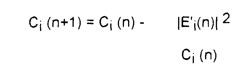
- errors are determined for a block of signals residual signals coming back in the time domain, errors that we compose to calculate a quadratic error that we pass in the frequency domain, in order to apply a set of corrections to lines of modulation, during the equalization of the carrier and the set of corrections to modulation lines by multiplication by a coefficient specific to each line, obtained by subtracting, at a previous coefficient, a complex number proportional to the error, in the frequency domain, relative to the line concerned and proportional to a signal combined with a signal representing the line considered just after transformation of the Fourier.
- the signals before transmission, are grouped together to be issued in blocks of fixed size which are each completed with a pattern circular and, in reception, the equalization in the frequency domain is applied to each block, after removing the circular pattern.
- the equalization in the frequency domain is applied to each block, after removing the circular pattern.
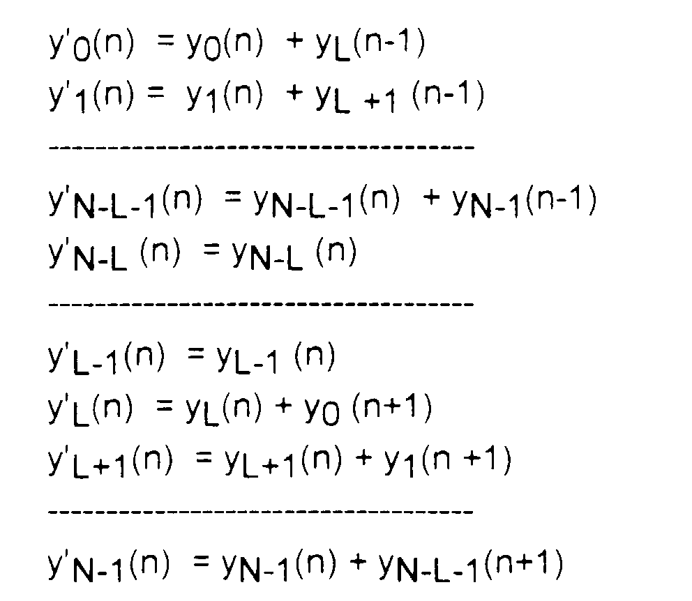
- the signals are grouped together received by blocks of fixed size only, after conversion into digital data. we complete each, at one end, by a fixed size sequence of numerical data of zero value overflowing in time on a block adjacent and, after equalization and return to the time domain, we summed term by term the equalized data which are in the areas of overlap and the corresponding equalized signals of the adjacent block temporally.
- the above compensation is in this case carried out after transmission, without need to perform transmission processing or recognize positions of blocks received.
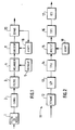
- the principle of the digital signal transmission method is illustrated by the block diagram of FIG. 1.
- the digital signals to be transmitted here by radio channel, are applied to a radio transmitter 1 to modulate a carrier frequency, the modulation occupying a frequency band surrounding the carrier. Filtering is provided here to limit the bandwidth necessary.
- the modulated carrier crosses the radio transmission channel 2 to reach a receiver 3 where it undergoes filtering tending to eliminate the out of band signals.
- the modulated carrier is then applied to a mixer 4 receiving the output of a free oscillator 5, oscillating at the frequency nominal of the carrier but not subject to it and therefore not following its variations, or drifts, possible.
- the carrier frequency at the output of mixer 4 is thus reduced to a zero or low frequency, and the baseband modulation thus obtained is applied to a frequency equalizer 11 supplying a digital demodulator 20 making decisions to recognize successive signals.
- Output of the demodulator 20 provides, to an adaptation circuit 18 of the equalizer 11, digital signals representing errors measured between the state of successive equalized signals, tainted with noise, and the corresponding expected state who was recognized.
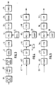
- FIG. 2 illustrates a first embodiment of the frequency equalizer 11.
- a sampling circuit 12 receives the modulated carrier and samples it with digitization of the samples, at the frequency 1 / T, T being the period of modulation, or symbol duration, during which a signal is transmitted.
- the successive sampled signals are presented in parallel by blocks of N signals (positive integer N) in a serial / parallel converter 13 connected to output to a calculation block 14 performing a direct discrete Fourier transformation over the set of N signals or sampling points.
- the calculation block 14 thus produces a spectrum of frequency lines.
- each line represented by numerical data
- a digital multiplier specific to the line, belonging to a set 15 of multipliers and whose complex multiplication coefficient is adjusted by in order to compensate for the attenuation and the phase shift undergone in the channel transmission 2 by the frequency modulation frequency component of the line considered.
- Carrier modulation by each signal, spread across the band transmitted and represented by the set of lines, is thus, as explained further on, cleared of distortions due to propagation in channel 2.
- the data of the block representing the amplitudes and phases of the lines as well equalized then undergo, in a calculation block 16, a transformation of Inverse discrete fourier which brings the modulated carrier back into the domain time, that is to say that each time signal is obtained from data representing the amplitudes and phases of the equalized lines.
- a parallel / serial digital converter 17 then transmits in series the time signals from the calculation block 16 to the digital demodulator 20.
- the adaptation circuit 18 receives, inter alia, in return from the demodulator 20 phase error information for adjusting the phase of the coefficients multiplier complexes 15.
- FIG. 3 A first variant of the transmission method is illustrated in FIG. 3.
- a compensation process is performed on transmission prior to this distortion.
- the signals to be transmitted are, by a blocking circuit 31, grouped by blocks of N points (N already defined) and, by a circuit 32, a circular prefix (or suffix) is added to each block.
- a block of N signals to transmit (a 0 , a 1 , .., a N-1 )
- a circular prefix of M symbols to form a block of length of M + N that the we are broadcasting.
- the pattern, prefix or suffix is said to be circular because it has successive influences, during convolution calculations, with each time a position shift.
- the signal from the mixer 4 passes through a low-pass filter 33 then a sampler 34 operating at the rate 1 / T, which transmits the received block (r 0 , r 1 , ..., r N + M-1 ) to a block synchronization circuit 35 which recognizes the position of each block and which removes the last M samples and transmits the block (r 0 , r 1 , ..., r N-1 ) obtained, thus pre-compensated, to the equalizer 11, for the passage in the frequency domain.
- This method of using a circular prefix (or suffix) makes the linear convolution of the transmission channel 2 equivalent to a circular convolution, therefore of the type applied to the discrete Fourier transformation.
- FIG. 4 A second variant of the transmission method, using a technique "overlay and addition” is illustrated in Figure 4.
- the carrier strip basic crosses a sampler-digitizer 42, of rate 1 / T, and arrives at a 43 point L / serial converter parallel feeding a block of calculation 44 of the frequency equalizer 41.
- the calculation block 44 also receives, for each block of L samples digitized, N-L additional digital data of value zero.
- This block is multiplied term by term, in the multipliers 45 controlled by the adaptation circuit 48, by a block (C0, C1, ..., CN-1) which represents the frequency response of the equalizer 41.
- the output of the equalizer 41 is the sum, calculated in a correction circuit 47, of the blocks of length N having the overlap on the NL points at the ends of the blocks.
- Equalization can thus work without a prefix or suffix, so without loss spectral efficiency of the modulated carrier.
- FIG. 5 illustrates a third variant of the transmission method, using a "recovery and selection" technique.
- the elements of FIG. 5 are homologous to those of FIG. 4 and the number of the units of their reference is the same, preceded by the tens.
- the circular convolution of the equalizer is reduced to a linear convolution. For this, every L modulation periods, we perform a discrete Fourier transformation providing a block (X 0 , X 1 , ..., X N-1 ) in the frequency domain from a time block (x 0 , X 1 , ..., x N-1 ) of received signals.
- the block (X 0 , X 1 , ..., X N-1 ) is multiplied term by term by the block of complex coefficients (C 0 , C 1 , ..., C N-1 ) representing the transfer function of the equalizer, which provides a frequency block (Y 0 , Y 1 , ..., Y N-1 ).
- the discrete inverse Fourier transformation transforms it into a time block of equalized signals (y 0 , y 1 , ..., y N-1 ) from the calculation block 56, from which is then eliminated, in the correction circuit. 57, the portion of the block corresponding to the temporal overlap zone between blocks, the convolution products of which are erroneous.
- FIG. 6 is a block diagram of the digital demodulator 20, located downstream of the equalizer 11 and successively receiving the equalized time signals y k .
- the demodulator 20 comprises a complex multiplier digital circuit 21 receiving the equalized temporal digital signals y k (k integer representing the temporal rank of the signal) and transforming them into corrected digital signals z k applied to a decision circuit 22.
- the decision circuit 22 compares the signal z k , and in particular its phase, with several digital signals representing the possible modulation states and chooses a signal â k estimated to be the one which differs the least from the corrected signal z k .
- Comparator 23 supplies a signal resulting from phase error ⁇ k which undergoes low-pass filtering in a digital filter 24, which can be transverse or recursive, before being applied, in the form of a signal u k , to a perfect accumulator 25.
- the accumulator 25 operates as an up or down counter and provides an angle value ⁇ k serving as an address for pointing a table of sines, cosine in read-only memory 26.
- the matching circuit 18 of the equalizer 11 operates from a block of predetermined signals (a 0 , a 1 , ..., a N-1 ), transmitted periodically after K-1 signal blocks (K integer positive), K being all the higher as the transmission channel 2 is stable.
- the predetermined block (A 0 , A 1 , ...; A N-1 ) corresponds to the discrete Fourier transform of the predetermined block (a 0 , a 1 , ..., a N-1 ).
- the coefficients C i A ' i / X i .
- FIG. 7 Another embodiment of the equalizer adaptation circuit is illustrated in FIG. 7.
- the signals y i (n) are transformed into the signals z i (n) in the demodulator 81 supplying the digital decision circuit 82, which supplies the digital signals a i (n) recognized.
- a i (n) is applied to a subtractor 84 receiving the signals y i (n) from the equalizer 71.
- the digital difference signals e ' i (n) y i (n) - e -j ⁇ i ( not) .
- a i (n) undergo, in a calculation block 85, a discrete Fourier transformation causing them to pass into the frequency domain and therefore determining an error E ' i (n) for each line of rank i .
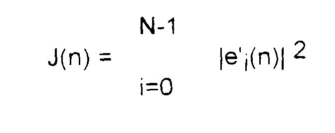
- the optimization of the coefficients C i of the equalizer 71 is then carried out, for each line i , by determining the time gradient of the function J (n). evolving as the blocks of successive time rank n are received .
- time / frequency and frequency / time transformations can be performed by any suitable algorithm and in particular by Fourier transformations modified.
Landscapes
- Engineering & Computer Science (AREA)
- Power Engineering (AREA)
- Computer Networks & Wireless Communication (AREA)
- Signal Processing (AREA)
- Cable Transmission Systems, Equalization Of Radio And Reduction Of Echo (AREA)
- Digital Transmission Methods That Use Modulated Carrier Waves (AREA)
- Reduction Or Emphasis Of Bandwidth Of Signals (AREA)
- Radar Systems Or Details Thereof (AREA)
- Networks Using Active Elements (AREA)
- Circuits Of Receivers In General (AREA)
- Measurement Of Velocity Or Position Using Acoustic Or Ultrasonic Waves (AREA)
- Testing, Inspecting, Measuring Of Stereoscopic Televisions And Televisions (AREA)
Description
- des moyens de calcul pour effectuer sur les signaux reçus une transformation de Fourier discrète directe fournissant un spectre de signaux de raies fréquentielles de la porteuse modulée,
- des moyens d'égalisation pour égaliser entre eux les signaux de raie en fonction de la distorsion de propagation estimée d'après un signal de référence,
- les moyens de calcul étant agencés pour appliquer au spectre des signaux de raies égalisés une transformation de Fourier discrète inverse et en fournir le résultat temporel aux moyens de décision ,
- la figure 1 est un schéma par blocs présentant la liaison de transmission de signaux numériques de l'invention,
- la figure 2 illustre un premier mode de réalisation de l'égaliseur fréquentiel du récepteur,
- les figures 3 à 5 illustrent respectivement trois variantes du procédé de transmission de l'invention,
- la figure 6 est un schéma synoptique du démodulateur numérique du récepteur et
- la figure 7 illustre un mode de réalisation de l'adaptation de coefficients correcteurs de l'égaliseur.


Claims (12)
- Procédé de transmission de signaux numériques, dans lequel on émet les signaux par modulation d'une fréquence porteuse et, en réception, on égalise (11), dans le domaine fréquentiel, les signaux reçus avant de les faire repasser dans le domaine temporel pour en effectuer le reconnaissance (20), caractérisé par le fait que, lors de l'étape de décision pour reconnaítre les signaux après égalisation, on mesure des erreurs de phase des signaux (εk) d'après des signaux antérieurs égalisés et on détermine des coefficients complexes de rotation de phase servant à l'égalisation (18) de signaux ultérieurs ainsi qu'à une correction (21) des phases des signaux temporels (yi (n)) ultérieurs, après leur égalisation.
- Procédé selon la revendication 1, dans lequel, on détermine, pour un bloc de signaux, des erreurs résiduelles (e'i(n)) des signaux venant de retourner dans le domaine temporel (yi(n)), erreurs que l'on compose pour calculer une erreur quadratique (J(n)) que l'on fait passer dans le domaine fréquentiel (85), afin d'appliquer (86) un ensemble de corrections à des raies de modulation, lors de l'égalisation de la porteuse modulée.
- Procédé selon la revendication 2, dans lequel on applique l'ensemble de corrections aux raies de modulation par multiplication par un coefficient (Ci (n + 1)) spécifique à chaque raie, obtenu en retranchant, à un coefficient antérieur (Ci (n)), un nombre complexe proportionnel à l'erreur (E'i,(n)), dans le domaine fréquentiel, relative à la raie concernée et proportionnel à un signal conjugué d'un signal (X*i (n)) d'un signal (Xi (n)) représentant la raie considérée juste après transformation de Fourier.
- Procédé selon l'une des revendications 1 à 3, dans lequel, par soustraction d'une fréquence (5) proche de celle de la porteuse et indépendante des variations de celle-ci, on transpose, avant égalisation, la porteuse reçue au voisinage d'une fréquence nulle.
- Procédé selon l'une des revendications 1 à 4, dans lequel, avant émission, on regroupe (31) les signaux à émettre par blocs de taille fixée que l'on complète (32) chacun par un motif circulaire et, en réception, l'égalisation dans le domaine fréquentiel est appliquée à chaque bloc, après en avoir ôté (35) le motif circulaire.
- Procédé selon l'une des revendications 1 à 4, dans lequel, en réception, on regroupe (43) les signaux reçus par blocs de taille fixée (L) que, après conversion en données numériques, on complète chacun, à une extrémité, par une séquence de taille fixée (N-L) de données numériques de valeur nulle débordant temporellement sur un bloc adjacent et, après égalisation et retour dans le domaine temporel, on additionne (47) terme à terme les données égalisées qui sont dans les zones de recouvrement et les signaux égalisés du bloc adjacent qui y correspondant temporellement.
- Procédé selon l'une des revendication 1 à 4, dans lequel, en réception, on regroupe les signaux par blocs de taille fixée (N) se recouvrant partiellement (N-L), avant d'effectuer l'égalisation (54-56) sur les blocs, et, après égalisation, on élimine (57) ceux (N-L) des signaux égalisés qui proviennent de signaux se trouvant dans la zone de recouvrement de deux blocs successifs.
- Récepteur de signaux numériques transmis par modulation d'une porteuse, comportant des moyens de décision (20) pour, en fonction des signaux reçus, prendre une décision de reconnaissance de signaux émis, comportantcaractérisé par le fait que les moyens de décision (20) comportent des moyens de rotation de phase (21) agencés pour transmettre, avec rotation de phase, les signaux temporels égalisés à des moyens (22, 23) de mesure d'erreurs de phase (εk) des dits signaux par rapport à des signaux de référence (âk), les moyens de mesure d'erreurs de phase (22, 23) étant agencés pour commander les moyens d'égalisation (15) et les moyens de rotation de phase (21).des moyens de calcul (14, 16) pour effectuer sur les signaux reçus une transformation de Fourier discrète directe fournissant un spectre de signaux de raies fréquentielles de la porteuse modulée,des moyens d'égalisation (15) pour égaliser entre eux les signaux de raie en fonction de la distorsion de propagation estimée d'après un signal de référence,les moyens de calcul (14, 16) étant agencés pour appliquer au spectre des signaux de raies égalisés une transformation de Fourier discrète inverse et en fournir le résultat temporel aux moyens de décision (20),
- Récepteur selon la revendication 8, dans lequel les moyens de décision (20) comportent un circuit accumulateur (25) agencé pour, en fonction des erreurs de phase (εk, uk), adresser une mémoire (26) contenant une table trigonométrique de réglage d'un circuit numérique multiplieur (21) transmettant lesdits signaux ultérieurs à un circuit de décision (22) fournissant lesdites erreurs (εk, uk).
- Récepteur selon l'une des revendications 8 et 9, dans lesquels les moyens de calcul sont agencés (35) pour, avant transformation de Fourier discrète directe, reconnaítre les positions de blocs de taille fixée des signaux reçus, comportant chacun un motif numérique circulaire, et pour en enlever ledit motif.
- Récepteur selon l'une des revendications 8 et 9, dans lequel les moyens de calcul sont agencés (43) pour regrouper les signaux reçus par blocs de taille fixée (L) et pour, après conversion en données numériques, compléter (43) chacun, à une extrémité, par une séquence de taille fixée (N-L) de données numériques de valeur nulle débordant temporellement sur un bloc adjacent, avant d'appliquer aux blocs complétés la transformation de Fourier discrète directe et pour additionner (47) terme à terme les données égalisées qui sont dans les zones de recouvrement et les signaux égalisés du bloc adjacent qui y correspondent temporellement.
- Récepteur selon l'une des revendications 8 et 9, dans lequel les moyens de calcul sont agencés (53) pour, avant la transformation de Fourier discrète, regrouper les signaux reçus par blocs de taille fixée (N) se recouvrant partiellement (N-L) dans le temps et pour, juste après la transformation de Fourier discrète inverse, éliminer (57) les signaux obtenus (N-L) provenant de signaux reçus appartenant à deux blocs.
Applications Claiming Priority (2)
| Application Number | Priority Date | Filing Date | Title |
|---|---|---|---|
| FR9313239A FR2712447B1 (fr) | 1993-11-08 | 1993-11-08 | Procédé de transmission de signaux numériques et récepteur pour la mise en Óoeuvre du procédé. |
| FR9313239 | 1993-11-08 |
Publications (2)
| Publication Number | Publication Date |
|---|---|
| EP0652663A1 EP0652663A1 (fr) | 1995-05-10 |
| EP0652663B1 true EP0652663B1 (fr) | 2000-03-29 |
Family
ID=9452589
Family Applications (1)
| Application Number | Title | Priority Date | Filing Date |
|---|---|---|---|
| EP94402488A Expired - Lifetime EP0652663B1 (fr) | 1993-11-08 | 1994-11-04 | Egalisateur fonctionnant en domaine fréquentiel |
Country Status (9)
| Country | Link |
|---|---|
| EP (1) | EP0652663B1 (fr) |
| AT (1) | ATE191305T1 (fr) |
| CZ (1) | CZ272994A3 (fr) |
| DE (1) | DE69423701T2 (fr) |
| FR (1) | FR2712447B1 (fr) |
| HU (1) | HU217739B (fr) |
| PL (1) | PL175643B1 (fr) |
| RU (1) | RU94040153A (fr) |
| SK (1) | SK132994A3 (fr) |
Families Citing this family (1)
| Publication number | Priority date | Publication date | Assignee | Title |
|---|---|---|---|---|
| WO2006008793A1 (fr) * | 2004-07-16 | 2006-01-26 | Fujitsu Limited | Procédé d’égalisation du domaine de fréquence et appareil récepteur à porteuse unique |
Family Cites Families (1)
| Publication number | Priority date | Publication date | Assignee | Title |
|---|---|---|---|---|
| US3679882A (en) * | 1970-06-11 | 1972-07-25 | Ibm | Fourier digital filter or equalizer and method of operation therefor |
-
1993
- 1993-11-08 FR FR9313239A patent/FR2712447B1/fr not_active Expired - Lifetime
-
1994
- 1994-11-02 HU HU9403146A patent/HU217739B/hu not_active IP Right Cessation
- 1994-11-04 RU RU94040153/09A patent/RU94040153A/ru unknown
- 1994-11-04 AT AT94402488T patent/ATE191305T1/de not_active IP Right Cessation
- 1994-11-04 EP EP94402488A patent/EP0652663B1/fr not_active Expired - Lifetime
- 1994-11-04 DE DE69423701T patent/DE69423701T2/de not_active Expired - Lifetime
- 1994-11-07 SK SK1329-94A patent/SK132994A3/sk unknown
- 1994-11-07 CZ CZ942729A patent/CZ272994A3/cs unknown
- 1994-11-08 PL PL94305753A patent/PL175643B1/pl unknown
Also Published As
| Publication number | Publication date |
|---|---|
| FR2712447B1 (fr) | 1996-01-05 |
| EP0652663A1 (fr) | 1995-05-10 |
| FR2712447A1 (fr) | 1995-05-19 |
| PL305753A1 (en) | 1995-05-15 |
| PL175643B1 (pl) | 1999-01-29 |
| SK132994A3 (en) | 1995-06-07 |
| DE69423701D1 (de) | 2000-05-04 |
| HU217739B (hu) | 2000-04-28 |
| HU9403146D0 (en) | 1994-12-28 |
| DE69423701T2 (de) | 2000-08-31 |
| ATE191305T1 (de) | 2000-04-15 |
| CZ272994A3 (en) | 1995-05-17 |
| HUT72795A (en) | 1996-05-28 |
| RU94040153A (ru) | 1996-09-27 |
Similar Documents
| Publication | Publication Date | Title |
|---|---|---|
| EP0125722B1 (fr) | Circuit d'égalisation adaptative et de démodulation conjointes | |
| EP0178720B1 (fr) | Dispositif de réception de données numériques comportant un dispositif de récupération adaptative de rythme | |
| EP0702866B1 (fr) | Paquet de signalisation pour systeme de communication avec reference modulee suivant une loi fonction du temps | |
| EP0013343B1 (fr) | Procédé et dispositif pour détecter une séquence pseudo-aléatoire de changements de phase de 0 degré et 180 degrés de la porteuse dans un récepteur de données | |
| US5539782A (en) | Digital data receiver | |
| EP0576359B1 (fr) | Procédé et dispositif égaliseur à retour de décisions pour la transmission par blocs de symboles d'information | |
| EP0762703A1 (fr) | Démodulation d'un signal multiporteur diminuant une distorsion blanche en fréquence | |
| EP0709959B1 (fr) | Correction d'un décalage de fréquence | |
| EP0012884B1 (fr) | Procédé et dispositif pour détecter une séquence pseudo-aléatoire de deux symboles dans un récepteur de données utilisant une modulation à double bande latérale-porteuse en quadrature | |
| EP0599722B1 (fr) | Dispositif de récupération du rythme baud dans un récepteur pour modem | |
| EP0376250B1 (fr) | Dispositif d'égalisation auto-adaptative pour installation de démodulation différentiellement cohérente | |
| EP0352159B1 (fr) | Procédé et dispositif de démodulation de signaux à enveloppe constante et phase continue modulés angulairement par un train de symboles binaires, tolérant les dérives de fréquence | |
| EP0140809B1 (fr) | Dispositif de correction d'échos, notamment pour système de télédiffusion de données | |
| LU82403A1 (fr) | Procede de compensation des bruits de phase a la reception d'une transmission de donnees | |
| EP0080544B1 (fr) | Procédé de réception d'un signal de données en modulation à double bande latérale-porteuses en quadrature | |
| EP0127544B1 (fr) | Annuleur d'écho à filtre numérique adaptatif pour système de transmission | |
| EP1074128B1 (fr) | Recepteur de signaux multiporteuse a correction de defauts d'egalisation provoques par les deplacements de la fenetre trf | |
| LU82402A1 (fr) | Procede de reduction des bruits de phase a la reception d'une transmission de donnees | |
| FR2786965A1 (fr) | Procede de recuperation de porteuse de signal | |
| EP0259419B1 (fr) | Double demodulateur numerique | |
| EP0652663A1 (fr) | Egalisateur fonctionnant en domaine fréquentiel | |
| CA2196209C (fr) | Procede de compensation des differences en temps de propagation de groupe entre les filtres analogiques d'un emetteur et ceux d'un recepteur de signaux en quadrature de phase, dispositif de compensation et systeme de transmission correspondants | |
| EP1142147B1 (fr) | Procede de reception de signaux a etalement de spectre avec correction de decalage en frequence | |
| EP0494003B1 (fr) | Un système récepteur pour le traitement de signaux reçus sur des voies de diversité | |
| EP0329049B1 (fr) | Procédé d'asservissement de l'instant de régénération dans une transmission numérique utilisant une modulation de porteuse selon deux axes en quadrature et dispositif de mise en oeuvre de ce procédé |
Legal Events
| Date | Code | Title | Description |
|---|---|---|---|
| PUAI | Public reference made under article 153(3) epc to a published international application that has entered the european phase |
Free format text: ORIGINAL CODE: 0009012 |
|
| AK | Designated contracting states |
Kind code of ref document: A1 Designated state(s): AT BE CH DE DK ES GB GR IE IT LI LU MC NL PT SE |
|
| RAX | Requested extension states of the european patent have changed |
Free format text: SI PAYMENT 941110 |
|
| 17P | Request for examination filed |
Effective date: 19950530 |
|
| 17Q | First examination report despatched |
Effective date: 19981012 |
|
| GRAG | Despatch of communication of intention to grant |
Free format text: ORIGINAL CODE: EPIDOS AGRA |
|
| GRAG | Despatch of communication of intention to grant |
Free format text: ORIGINAL CODE: EPIDOS AGRA |
|
| GRAH | Despatch of communication of intention to grant a patent |
Free format text: ORIGINAL CODE: EPIDOS IGRA |
|
| GRAH | Despatch of communication of intention to grant a patent |
Free format text: ORIGINAL CODE: EPIDOS IGRA |
|
| GRAA | (expected) grant |
Free format text: ORIGINAL CODE: 0009210 |
|
| AK | Designated contracting states |
Kind code of ref document: B1 Designated state(s): AT BE CH DE DK ES GB GR IE IT LI LU MC NL PT SE |
|
| AX | Request for extension of the european patent |
Free format text: SI PAYMENT 19941110 |
|
| PG25 | Lapsed in a contracting state [announced via postgrant information from national office to epo] |
Ref country code: SE Free format text: THE PATENT HAS BEEN ANNULLED BY A DECISION OF A NATIONAL AUTHORITY Effective date: 20000329 Ref country code: IT Free format text: LAPSE BECAUSE OF FAILURE TO SUBMIT A TRANSLATION OF THE DESCRIPTION OR TO PAY THE FEE WITHIN THE PRE;WARNING: LAPSES OF ITALIAN PATENTS WITH EFFECTIVE DATE BEFORE 2007 MAY HAVE OCCURRED AT ANY TIME BEFORE 2007. THE CORRECT EFFECTIVE DATE MAY BE DIFFERENT FROM THE ONE RECORDED.SCRIBED TIME-LIMIT Effective date: 20000329 Ref country code: GR Free format text: LAPSE BECAUSE OF NON-PAYMENT OF DUE FEES Effective date: 20000329 Ref country code: ES Free format text: THE PATENT HAS BEEN ANNULLED BY A DECISION OF A NATIONAL AUTHORITY Effective date: 20000329 Ref country code: AT Free format text: LAPSE BECAUSE OF FAILURE TO SUBMIT A TRANSLATION OF THE DESCRIPTION OR TO PAY THE FEE WITHIN THE PRESCRIBED TIME-LIMIT Effective date: 20000329 |
|
| REF | Corresponds to: |
Ref document number: 191305 Country of ref document: AT Date of ref document: 20000415 Kind code of ref document: T |
|
| REG | Reference to a national code |
Ref country code: CH Ref legal event code: EP |
|
| REG | Reference to a national code |
Ref country code: IE Ref legal event code: FG4D Free format text: FRENCH |
|
| REF | Corresponds to: |
Ref document number: 69423701 Country of ref document: DE Date of ref document: 20000504 |
|
| PG25 | Lapsed in a contracting state [announced via postgrant information from national office to epo] |
Ref country code: PT Free format text: LAPSE BECAUSE OF FAILURE TO SUBMIT A TRANSLATION OF THE DESCRIPTION OR TO PAY THE FEE WITHIN THE PRESCRIBED TIME-LIMIT Effective date: 20000629 Ref country code: DK Free format text: LAPSE BECAUSE OF FAILURE TO SUBMIT A TRANSLATION OF THE DESCRIPTION OR TO PAY THE FEE WITHIN THE PRESCRIBED TIME-LIMIT Effective date: 20000629 |
|
| GBT | Gb: translation of ep patent filed (gb section 77(6)(a)/1977) |
Effective date: 20000616 |
|
| PG25 | Lapsed in a contracting state [announced via postgrant information from national office to epo] |
Ref country code: LU Free format text: LAPSE BECAUSE OF NON-PAYMENT OF DUE FEES Effective date: 20001104 |
|
| PG25 | Lapsed in a contracting state [announced via postgrant information from national office to epo] |
Ref country code: MC Free format text: THE PATENT HAS BEEN ANNULLED BY A DECISION OF A NATIONAL AUTHORITY Effective date: 20001130 Ref country code: LI Free format text: LAPSE BECAUSE OF NON-PAYMENT OF DUE FEES Effective date: 20001130 Ref country code: CH Free format text: LAPSE BECAUSE OF NON-PAYMENT OF DUE FEES Effective date: 20001130 Ref country code: BE Free format text: LAPSE BECAUSE OF NON-PAYMENT OF DUE FEES Effective date: 20001130 |
|
| PLBE | No opposition filed within time limit |
Free format text: ORIGINAL CODE: 0009261 |
|
| STAA | Information on the status of an ep patent application or granted ep patent |
Free format text: STATUS: NO OPPOSITION FILED WITHIN TIME LIMIT |
|
| PG25 | Lapsed in a contracting state [announced via postgrant information from national office to epo] |
Ref country code: IE Free format text: LAPSE BECAUSE OF NON-PAYMENT OF DUE FEES Effective date: 20010205 |
|
| REG | Reference to a national code |
Ref country code: IE Ref legal event code: FD4D |
|
| 26N | No opposition filed | ||
| BERE | Be: lapsed |
Owner name: SAT S.A. Effective date: 20001130 |
|
| REG | Reference to a national code |
Ref country code: CH Ref legal event code: PL |
|
| REG | Reference to a national code |
Ref country code: GB Ref legal event code: IF02 |
|
| REG | Reference to a national code |
Ref country code: GB Ref legal event code: 732E Free format text: REGISTERED BETWEEN 20090319 AND 20090325 |
|
| REG | Reference to a national code |
Ref country code: GB Ref legal event code: 732E Free format text: REGISTERED BETWEEN 20090326 AND 20090401 |
|
| REG | Reference to a national code |
Ref country code: GB Ref legal event code: 732E Free format text: REGISTERED BETWEEN 20110421 AND 20110427 |
|
| REG | Reference to a national code |
Ref country code: GB Ref legal event code: 732E Free format text: REGISTERED BETWEEN 20110428 AND 20110504 |
|
| REG | Reference to a national code |
Ref country code: GB Ref legal event code: 732E Free format text: REGISTERED BETWEEN 20110505 AND 20110511 |
|
| PGFP | Annual fee paid to national office [announced via postgrant information from national office to epo] |
Ref country code: DE Payment date: 20131022 Year of fee payment: 20 Ref country code: GB Payment date: 20131025 Year of fee payment: 20 |
|
| PGFP | Annual fee paid to national office [announced via postgrant information from national office to epo] |
Ref country code: NL Payment date: 20131023 Year of fee payment: 20 |
|
| REG | Reference to a national code |
Ref country code: DE Ref legal event code: R071 Ref document number: 69423701 Country of ref document: DE |
|
| REG | Reference to a national code |
Ref country code: DE Ref legal event code: R071 Ref document number: 69423701 Country of ref document: DE |
|
| REG | Reference to a national code |
Ref country code: NL Ref legal event code: V4 Effective date: 20141104 |
|
| REG | Reference to a national code |
Ref country code: GB Ref legal event code: PE20 Expiry date: 20141103 |
|
| PG25 | Lapsed in a contracting state [announced via postgrant information from national office to epo] |
Ref country code: GB Free format text: LAPSE BECAUSE OF EXPIRATION OF PROTECTION Effective date: 20141103 |