EP0651585B1 - Analog circuit controller using signals indicative of control voltage and type of control voltage - Google Patents
Analog circuit controller using signals indicative of control voltage and type of control voltage Download PDFInfo
- Publication number
- EP0651585B1 EP0651585B1 EP19940116838 EP94116838A EP0651585B1 EP 0651585 B1 EP0651585 B1 EP 0651585B1 EP 19940116838 EP19940116838 EP 19940116838 EP 94116838 A EP94116838 A EP 94116838A EP 0651585 B1 EP0651585 B1 EP 0651585B1
- Authority
- EP
- European Patent Office
- Prior art keywords
- control voltage
- analog circuit
- control
- converter
- microcomputer
- Prior art date
- Legal status (The legal status is an assumption and is not a legal conclusion. Google has not performed a legal analysis and makes no representation as to the accuracy of the status listed.)
- Expired - Lifetime
Links
- 230000005540 biological transmission Effects 0.000 description 5
- 238000006243 chemical reaction Methods 0.000 description 5
- 238000000034 method Methods 0.000 description 4
- 230000008054 signal transmission Effects 0.000 description 3
- 230000002411 adverse Effects 0.000 description 2
- 238000010586 diagram Methods 0.000 description 2
- 230000007704 transition Effects 0.000 description 2
- 239000003990 capacitor Substances 0.000 description 1
- 230000002401 inhibitory effect Effects 0.000 description 1
Images


Classifications
-
- H—ELECTRICITY
- H04—ELECTRIC COMMUNICATION TECHNIQUE
- H04B—TRANSMISSION
- H04B1/00—Details of transmission systems, not covered by a single one of groups H04B3/00 - H04B13/00; Details of transmission systems not characterised by the medium used for transmission
- H04B1/06—Receivers
- H04B1/16—Circuits
- H04B1/20—Circuits for coupling gramophone pick-up, recorder output, or microphone to receiver
- H04B1/202—Circuits for coupling gramophone pick-up, recorder output, or microphone to receiver by remote control
-
- H—ELECTRICITY
- H04—ELECTRIC COMMUNICATION TECHNIQUE
- H04N—PICTORIAL COMMUNICATION, e.g. TELEVISION
- H04N5/00—Details of television systems
- H04N5/44—Receiver circuitry for the reception of television signals according to analogue transmission standards
Definitions
- Fig. 4 shows waveforms illustrating the operation of the analog circuit according to the present invention.
Landscapes
- Engineering & Computer Science (AREA)
- Signal Processing (AREA)
- Multimedia (AREA)
- Computer Networks & Wireless Communication (AREA)
- Analogue/Digital Conversion (AREA)
Description
- The present invention relates to an analog circuit controller and particularly a controller for controlling a plurality of analog circuits in an analog IC through two different analog signals.
- TV receivers and audio instruments may control an IC for processing analog signals through control signals from a microcomputer. In a TV receiver, for example, commands from a TV viewer which are indicative of tint, color density and others, in television signals, may be temporarily taken by a micro computer and then applied from the microcomputer to an analog IC.
- One of such controllers is shown in Fig. 1. It comprises a
microcomputer 1 including a plurality of PWM (Pulse Width Modulation) circuits 2-4 located therewithin and integrating circuits 5-7 for converting the modulated pulses from the PWM circuits into analog signals which are in turn applied to circuits to be controlled 9-11 in an analog IC (8). However, the controller of Fig. 1 requires one control line for every control function to be carried out. If the number of pins in the microcomputer and IC is increased, the wiring in such a controller will become undesirably complicated. - To overcome such a problem, there has been proposed a method of time dividing digital signals and transmitting the divided digital signal through clock and data lines, as shown in Fig. 2. Digital data are applied from a
microcomputer 1 to ananalog IC 8 in synchronism with clock signals. Theanalog IC 8 includes anaddress control circuit 12 for decoding the incoming digital data and for judging which circuit to be controlled the data are to be transmitted to, so that the digital data will be distributed to an appropriate circuit to be controlled. The digital data are converted into analog signals through D/A conversion circuits 13-15 before they are applied to circuits to be controlled 9-11. - The method of Fig. 2 can transmit different types of control signals through only two signal lines. However, the method of Fig. 2 requires a plurality of D/A conversion circuits 13-15 in the
analog IC 8. In general, an analog IC having many D/A conversion circuits, each of which is also formed having an increased number of elements, raises a problem in that the chip area increases. - On the other hand, the
microcomputer 1 is formed by MOSIC and therefore does not raise any problem even if there are many D/A conversion circuits. It is therefore desired that a transmission process for performing the D/A conversion in the microcomputer using less signal lines is provided. - From GB-A-22 47 547 a microcomputer is known comprising two D/A converters, each of which has an output which can assume various levels. The outputs of these D/A converters represent statuses of the microcomputer both representing the same kind of characteristics.
- It is an object of the present invention to provide a microcomputer and an analog circuit controller needing a minimum amount of signal lines and D/A converters for performing a control of a plurality of circuits in an analog IC.
- This object is solved by the features of the appended claims.
- In the described embodiment control data are input to the first D/A converter and switching data are input to the second D/A converter, so that the output of the first converter determines a voltage which is held by one of the plurality of DC hold circuits. Additionally a switching control controls the function of the corresponding circuits. Thus the output of the second D/A converter determines where the output of the first converter is to be applied to. In the described embodiment there are three DC hold circuits provided and the output of the second D/A converter designates one of those DC hold circuits.
- Fig. 1 is a view of an analog circuit controller constructed according to the prior art.
- Fig. 2 is a view of another analog circuit controller constructed according to the prior art.
- Fig. 3 is a view of an analog circuit controller constructed according to the present invention.
- Fig. 4 shows waveforms illustrating the operation of the analog circuit according to the present invention.
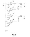
- Fig. 5 is a circuit diagram showing the details of the comparison/switching control circuit in the analog circuit of the present invention.
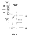
- Fig. 6 is a view showing the details of the waveforms in Fig. 4.
- Fig. 3 shows a controller according to the present invention which comprises a first D/
A converter 16 for generating a TV signal control voltage variable into a plurality of levels in a time-divided manner, a second D/A converter 17 for generating switching signals each indicative of the type of the control voltage in synchronism with the time-division timing for the control voltage, first to third DC holdcircuits A converter 16 and for applying a DC voltage held by the DC hold circuit itself to the corresponding one of first to third circuits to be controlled 9, 10 and 11, a comparison/switching control circuit 21 including a plurality of comparators and being operative to discriminate the level of a switching signal from the second D/A converter 17 and to actuate the corresponding one of said DC hold circuits,filters DC hold circuits deflection circuit 24 for applying vertical pulses in TV signals to avertical output IC 25 and themicrocomputer 1, a Brauntube 27 having a deflection coil (26) for receiving vertical deflection pulses from saidvertical output IC 25, and first andsecond input terminals - Fig. 4 shows waveforms illustrating the operation of this embodiment. The upper part of Fig. 4 shows various levels of output signal from the second D/
A converter 17 while the lower part thereof shows various levels of output signal from the first D/A converter 16. The horizontal axes of Fig. 4 represent time, and with the passage of time, the tint, color and contrast in TV signals are controlled. - The tint will be described first. The level of a tint switching signal generated by the second D/
A converter 17 is set at any level within a range between 0.5V and 1.0V. In this embodiment, it is 0.75V. During a period in which the tint switching signal of 0.75V is generated, the first D/A converter 16 generates a control voltage of 2V which is in turn applied to the first to third DC hold circuits 18-20 in theanalog IC 8. On the other hand, the comparison/switching control circuit 21 distinguishes from the level of the 0.75V switching signal that the incoming control voltage is a tint control signal, and actuates only the firstDC hold circuit 18. Thus, the firstDC hold circuit 18 holds the 2V control voltage which is in turn applied to the first circuit to be controlled 9. As a result, the tint can be controlled according to this embodiment. - The system of Fig. 3 executes a plurality of controls with the passage of time. In general, therefore, another control (e.g., for brightness) will be carried out before the first
DC hold circuit 18 holds the 2V control voltage. If the level of one control voltage is greatly different from that of the next control voltage, time may be required at the transition between these two control voltages under influence of the time constant in thefilter 22. According to the present invention, thus, a time period during which the first to third DC hold circuits 18-20 are inhibited to hold the input voltage is provided at the boundary between two time-divided controls. Since the next control voltage is applied from the first D/A converter 16 to the pins of theanalog IC 8 even during such a time period, the control voltage can stably be taken in after termination of the inhibiting period. With the tint control, the second D/A converter 17 generates a control voltage of 0.25V before the 0.75V control voltage is generated, as shown in Fig. 4. As the 0.25V control voltage is applied to the comparison/switching control circuit 21, the latter inhibits the first to third DC hold circuits 18-20 from taking inputs in. - Fig. 5 is a circuit diagram showing the details of the comparison/
switching control circuit 21 of Fig. 3. It is now assumed that a switching signal of 0.75V is applied to theinput terminal 24 during the tint control period of Fig: 4. The reference voltages 29-32 of the first to fourth comparators 25-28 are set at 0.5V, 1V, 1.5V and 2.0V, respectively. Thus, only the output of thefirst comparator 25 is at [H] level while the outputs of all the other comparators are at [L] level. As a result, theoutput terminal 33 becomes [H] level during which only theswitch 34 of the firstDC hold circuit 18 is closed. In other words, the first andsecond comparators inverter 35 and anAND gate 36 to form a window comparator and detects the input voltage being between 0.5V and 1.0V, as a [H] level. - If a switching signal of 0.25V is applied to the
input terminal 24, the levels of both theoutput terminals - The process proceeds to the color control step. A switching signal of 1.25V is applied to the
input terminal 24 shown in Fig. 5. Theoutput terminals input terminal 24, only theoutput terminal 37 becomes [H] level so that the second DC hold circuit 19 of Fig. 3 takes a control voltage of 3V shown in Fig. 4. As a result, the color control voltage can be applied to the second circuit to be controlled 10. The contrast control can be carried out in the similar manner. - The transmission of a signal from the
microcomputer 1 to theanalog IC 8 should not be carried out during a period in which a TV scene image is displayed. This is because EMI noise from the pins adversely affects the image signals in the TV scene since pulsed signals are transmitted through the pins of the IC. The first to third DC hold circuits 18-20 in theanalog IC 8 cannot stop their operations immediately after termination of the DC taking-in period, but will slightly discharge the charges in the charged capacitor. Thus, a DC signal having a DC offset appears at the output of the DC hold circuits. Such a DC offset changes the degree of control relative to the circuits to be controlled in theanalog IC 8. Thus, the DC offset will directly influence the TV scene. - According to the present invention, therefore, the transmission of a signal will be carried out only during a period in which no image will be displayed in the TV scene. There is no problem even if EMI noise is generated through the IC pins and further, even though an offset is generated in the initial value of a DC voltage to be transmitted, so long as the final value thereof is fixed, there is no problem.
- The embodiment of Fig. 3 will now be described. This embodiment performs the transmission of a signal only during the vertical pulse period. Vertical pulses generated by the
deflection circuit 24 in theanalog IC 8 are applied to thevertical output IC 25 and then to thevertical deflection coil 26 in theBraun tube 27. The vertical pulses are also taken in by themicrocomputer 1 which in turn uses them as triggers to generate the switching signal and control voltage shown in Fig. 4. During the vertical pulse period, each of the first to third DC hold circuits 18-20 may make one control or two or more controls, if necessary. - Fig. 6 shows the details of the waveform shown in Fig. 4. The upper part of Fig. 6 represents a switching signal while the lower part thereof denotes a control voltage. At time t1, when a vertical pulse reaches its lowest level, the
microcomputer 1 recognizes the arrival of the vertical pulse. At time t2, after a predetermined time period, a control voltage is first generated. At time t3, whereat it is expected that the control voltage is stabilized, a switching signal is transmitted to the comparison/switching control circuit. Thus, the system can take in a stable voltage (2V). At time t4, the switching signal enters the range of tint (from 0.5V to 1.0V) so that the voltage (2V) will be taken in by the system. The taking-in operation continues until time t5, where said range of tint is exceeded. At time t6 after a predetermined period from the time t5, the transition of the control voltage is initiated. These times may previously be computed and programmed in themicrocomputer 1 so as to be able to perform a stabilized transmission of control voltage. - Such a transmission may be carried out without vertical pulses. If the transmission is to be made through the vertical pulse, however, it is only necessary to decide the final voltage to be held without considering the order of t3 and t4 shown in Fig. 6.
- As described above, the system can be formed by fewer elements since the microcomputer includes the D/A converters and the comparison/switching control circuit is disposed in the analog IC. According to the present invention, further, any adverse affects on a TV scene can be prevented since the transmission of the control voltage is carried out only during the vertical pulse period.
Claims (4)
- An analog circuit controller using an external control voltage to control a plurality of circuits (9-11) to be controlled, comprising:a first input terminal (38) to which a control voltage is applied in a time divided manner the level of which assumes predetermined values during predetermined time periods (TA);a second input terminal (39) for receiving a switching signal in synchronism with the time division timing for said control voltage, the level of said switching signal during a predetermined time period (TA) being indicative of the type of the control voltage in said period (TA);a plurality of DC hold circuits (18,19,20) each for holding the control voltage applied thereto through said first input terminal (38) as a DC voltage and for applying said DC voltage to a corresponding circuit (9 to 11) to be controlled; anda comparison/switching control circuit (21) including a plurality of comparators (25 to 28) for determining to which DC hold circuit (18 to 20) the control voltage at the first input terminal (38) is supplied in accordance with the switching signal at the second input terminal (39).
- An analog circuit control system characterized by an analog circuit controller as defined in claim 1 further comprising a microcomputer;said microcomputer outputting a control voltage from a first D/A converter (16) at a time divided timing, said control voltage assuming predetermined levels during predetermined time periods TA, andsaid microcomputer outputs a switching signal from a second D/A converter (17) synchronous with said time divided timing of said control voltage, the level of said switching signal during a predetermined time period (TA) being representative of the type of said control voltage output during said predetermined time period (TA), whereby said output of the second D/A converter is correlated in time during said time periods (TA) with said output of the first D/A converter;wherein the output of the first D/A converter (16) in said microcomputer (1) is connected to the first input terminal (38) of said analog circuit controller (8) and the second D/A converter (17) is connected to the second input terminal (39).
- An analog circuit control system according to claim 2 wherein a signal having a level inhibiting the DC hold circuits (18-20) of said analog circuit controller (8) from holding the control voltage is inserted into said switching signal between said time periods (TA).
- An analog circuit control system according to claim 2 wherein said analog IC applies a TV signal vertical pulse to said microcomputer (1), wherein said microcomputer (1) transmits said control voltage and the corresponding switching voltage to the analog circuit controller during a period in which said vertical pulse is applied.
Applications Claiming Priority (6)
| Application Number | Priority Date | Filing Date | Title |
|---|---|---|---|
| JP27236893 | 1993-10-29 | ||
| JP27236893A JP2957866B2 (en) | 1993-10-29 | 1993-10-29 | Control device for analog circuit using microcomputer |
| JP272368/93 | 1993-10-29 | ||
| JP28824793A JP2957867B2 (en) | 1993-11-17 | 1993-11-17 | Control device for analog circuit |
| JP28824793 | 1993-11-17 | ||
| JP288247/93 | 1993-11-17 |
Publications (2)
| Publication Number | Publication Date |
|---|---|
| EP0651585A1 EP0651585A1 (en) | 1995-05-03 |
| EP0651585B1 true EP0651585B1 (en) | 1999-09-08 |
Family
ID=26550164
Family Applications (1)
| Application Number | Title | Priority Date | Filing Date |
|---|---|---|---|
| EP19940116838 Expired - Lifetime EP0651585B1 (en) | 1993-10-29 | 1994-10-25 | Analog circuit controller using signals indicative of control voltage and type of control voltage |
Country Status (4)
| Country | Link |
|---|---|
| US (1) | US5872603A (en) |
| EP (1) | EP0651585B1 (en) |
| KR (1) | KR0147016B1 (en) |
| DE (1) | DE69420510T2 (en) |
Families Citing this family (5)
| Publication number | Priority date | Publication date | Assignee | Title |
|---|---|---|---|---|
| JP3758849B2 (en) * | 1998-04-28 | 2006-03-22 | ローム株式会社 | Data converter |
| CA2581941C (en) † | 2004-09-27 | 2012-08-21 | Unitron | Electronic filter device for the reception of tv-signals |
| KR100747271B1 (en) * | 2006-02-06 | 2007-08-07 | 기아자동차주식회사 | Aluminum cylinder block of automobile engine |
| TWI316794B (en) * | 2006-06-15 | 2009-11-01 | Mstar Semiconductor Inc | Digital-to-analog converter and related method |
| CN101141130B (en) * | 2006-09-04 | 2011-06-01 | 晨星半导体股份有限公司 | Digital-to-analog converter and related methods |
Citations (1)
| Publication number | Priority date | Publication date | Assignee | Title |
|---|---|---|---|---|
| GB2247547A (en) * | 1990-08-31 | 1992-03-04 | Mitsubishi Electric Corp | Internal state monitoring in a microcomputer |
Family Cites Families (9)
| Publication number | Priority date | Publication date | Assignee | Title |
|---|---|---|---|---|
| FR2278120A1 (en) * | 1974-07-08 | 1976-02-06 | Cit Alcatel | DESIGNATION DEVICE FOR AN ELEMENT OF AN IMAGE |
| JPS59116995A (en) * | 1982-12-23 | 1984-07-06 | Toshiba Eng Co Ltd | Writing device of analog hold circuit |
| US4879625A (en) * | 1987-12-11 | 1989-11-07 | Potenzone Richard A | Voltage monitor |
| JPH02287933A (en) * | 1989-04-27 | 1990-11-28 | Matsushita Electric Ind Co Ltd | Semiconductor laser driving circuit |
| JPH0338703A (en) * | 1989-07-05 | 1991-02-19 | Yokogawa Electric Corp | Analog signal input/output device |
| US5231475A (en) * | 1990-02-16 | 1993-07-27 | Videotek, Inc. | Method and apparatus for generating video signal representing controllable color matte |
| US5262680A (en) * | 1991-07-08 | 1993-11-16 | Industrial Technology Research Institute | Switch control apparatus for eliminating intermittent on/off condition on a power supply switch |
| US5239243A (en) * | 1992-10-01 | 1993-08-24 | Alliant Techsystems, Inc., | CRT beam deflection system |
| JP3038703U (en) | 1996-12-12 | 1997-06-24 | 日本エービーエス株式会社 | Anti-skid controller for motorcycles |
-
1994
- 1994-09-22 US US08/310,405 patent/US5872603A/en not_active Expired - Lifetime
- 1994-10-25 DE DE69420510T patent/DE69420510T2/en not_active Expired - Fee Related
- 1994-10-25 EP EP19940116838 patent/EP0651585B1/en not_active Expired - Lifetime
- 1994-10-28 KR KR1019940027848A patent/KR0147016B1/en not_active Expired - Fee Related
Patent Citations (1)
| Publication number | Priority date | Publication date | Assignee | Title |
|---|---|---|---|---|
| GB2247547A (en) * | 1990-08-31 | 1992-03-04 | Mitsubishi Electric Corp | Internal state monitoring in a microcomputer |
Also Published As
| Publication number | Publication date |
|---|---|
| KR0147016B1 (en) | 1998-09-15 |
| DE69420510D1 (en) | 1999-10-14 |
| DE69420510T2 (en) | 2000-04-27 |
| EP0651585A1 (en) | 1995-05-03 |
| US5872603A (en) | 1999-02-16 |
| KR950013205A (en) | 1995-05-17 |
Similar Documents
| Publication | Publication Date | Title |
|---|---|---|
| CA2131711C (en) | Auxiliary video data slicer | |
| US5654743A (en) | Picture display arrangement | |
| USRE38890E1 (en) | Device for converting data using look-up tables | |
| EP0455957A2 (en) | Odd/even field detector for video signals | |
| EP0366124B1 (en) | Field discrimination circuit | |
| US5872603A (en) | Analog circuit controller using signals indicative of control voltage and type of control voltage | |
| US4743968A (en) | Electronic apparatus control system | |
| CA2318934A1 (en) | Line driver with linear transitions | |
| US20030193462A1 (en) | Display device and interface circuit for the display device | |
| US5489946A (en) | High speed sync separation system and method | |
| EP0185096B1 (en) | Apparatus for controlling amplitude of vertically deflecting signals | |
| CN1098479C (en) | Analog circuit controller | |
| US5754071A (en) | Digital signal delaying method and circuit | |
| JP2957867B2 (en) | Control device for analog circuit | |
| US4360825A (en) | Vertical drive generator and horizontal rate gate generator for a television receiver | |
| JP2957866B2 (en) | Control device for analog circuit using microcomputer | |
| JP3043242B2 (en) | Control device for analog circuit | |
| JPS6319987A (en) | Video signal processing circuit | |
| JP2957989B1 (en) | Display device | |
| US4506297A (en) | Integrated circuit for television receivers comprising a sonic separator with a clamping circuit | |
| US6052075A (en) | Data processing device having a D/A function | |
| JP3081554B2 (en) | Control device for analog circuit using microcomputer | |
| JPH07143005A (en) | Controller for analog circuit | |
| JPH05299987A (en) | Automatic identification level controller | |
| JPS6335135B2 (en) |
Legal Events
| Date | Code | Title | Description |
|---|---|---|---|
| PUAI | Public reference made under article 153(3) epc to a published international application that has entered the european phase |
Free format text: ORIGINAL CODE: 0009012 |
|
| AK | Designated contracting states |
Kind code of ref document: A1 Designated state(s): DE FR GB |
|
| 17P | Request for examination filed |
Effective date: 19950530 |
|
| 17Q | First examination report despatched |
Effective date: 19970522 |
|
| GRAG | Despatch of communication of intention to grant |
Free format text: ORIGINAL CODE: EPIDOS AGRA |
|
| GRAG | Despatch of communication of intention to grant |
Free format text: ORIGINAL CODE: EPIDOS AGRA |
|
| GRAH | Despatch of communication of intention to grant a patent |
Free format text: ORIGINAL CODE: EPIDOS IGRA |
|
| GRAH | Despatch of communication of intention to grant a patent |
Free format text: ORIGINAL CODE: EPIDOS IGRA |
|
| GRAA | (expected) grant |
Free format text: ORIGINAL CODE: 0009210 |
|
| AK | Designated contracting states |
Kind code of ref document: B1 Designated state(s): DE FR GB |
|
| REF | Corresponds to: |
Ref document number: 69420510 Country of ref document: DE Date of ref document: 19991014 |
|
| ET | Fr: translation filed | ||
| PLBE | No opposition filed within time limit |
Free format text: ORIGINAL CODE: 0009261 |
|
| STAA | Information on the status of an ep patent application or granted ep patent |
Free format text: STATUS: NO OPPOSITION FILED WITHIN TIME LIMIT |
|
| 26N | No opposition filed | ||
| REG | Reference to a national code |
Ref country code: GB Ref legal event code: IF02 |
|
| PGFP | Annual fee paid to national office [announced via postgrant information from national office to epo] |
Ref country code: DE Payment date: 20081027 Year of fee payment: 15 |
|
| PG25 | Lapsed in a contracting state [announced via postgrant information from national office to epo] |
Ref country code: DE Free format text: LAPSE BECAUSE OF NON-PAYMENT OF DUE FEES Effective date: 20100501 |
|
| PGFP | Annual fee paid to national office [announced via postgrant information from national office to epo] |
Ref country code: GB Payment date: 20120925 Year of fee payment: 19 |
|
| PGFP | Annual fee paid to national office [announced via postgrant information from national office to epo] |
Ref country code: FR Payment date: 20121010 Year of fee payment: 19 |
|
| GBPC | Gb: european patent ceased through non-payment of renewal fee |
Effective date: 20131025 |
|
| PG25 | Lapsed in a contracting state [announced via postgrant information from national office to epo] |
Ref country code: GB Free format text: LAPSE BECAUSE OF NON-PAYMENT OF DUE FEES Effective date: 20131025 |
|
| REG | Reference to a national code |
Ref country code: FR Ref legal event code: ST Effective date: 20140630 |
|
| PG25 | Lapsed in a contracting state [announced via postgrant information from national office to epo] |
Ref country code: FR Free format text: LAPSE BECAUSE OF NON-PAYMENT OF DUE FEES Effective date: 20131031 |