EP0650093B1 - Polysilane type photosensitive resin composition and method for forming pattern using the same - Google Patents
Polysilane type photosensitive resin composition and method for forming pattern using the same Download PDFInfo
- Publication number
- EP0650093B1 EP0650093B1 EP94307644A EP94307644A EP0650093B1 EP 0650093 B1 EP0650093 B1 EP 0650093B1 EP 94307644 A EP94307644 A EP 94307644A EP 94307644 A EP94307644 A EP 94307644A EP 0650093 B1 EP0650093 B1 EP 0650093B1
- Authority
- EP
- European Patent Office
- Prior art keywords
- sol
- polysilane
- photosensitive layer
- pattern
- resin composition
- Prior art date
- Legal status (The legal status is an assumption and is not a legal conclusion. Google has not performed a legal analysis and makes no representation as to the accuracy of the status listed.)
- Expired - Lifetime
Links
Images

Classifications
-
- G—PHYSICS
- G03—PHOTOGRAPHY; CINEMATOGRAPHY; ANALOGOUS TECHNIQUES USING WAVES OTHER THAN OPTICAL WAVES; ELECTROGRAPHY; HOLOGRAPHY
- G03F—PHOTOMECHANICAL PRODUCTION OF TEXTURED OR PATTERNED SURFACES, e.g. FOR PRINTING, FOR PROCESSING OF SEMICONDUCTOR DEVICES; MATERIALS THEREFOR; ORIGINALS THEREFOR; APPARATUS SPECIALLY ADAPTED THEREFOR
- G03F7/00—Photomechanical, e.g. photolithographic, production of textured or patterned surfaces, e.g. printing surfaces; Materials therefor, e.g. comprising photoresists; Apparatus specially adapted therefor
- G03F7/004—Photosensitive materials
- G03F7/075—Silicon-containing compounds
- G03F7/0754—Non-macromolecular compounds containing silicon-to-silicon bonds
-
- G—PHYSICS
- G03—PHOTOGRAPHY; CINEMATOGRAPHY; ANALOGOUS TECHNIQUES USING WAVES OTHER THAN OPTICAL WAVES; ELECTROGRAPHY; HOLOGRAPHY
- G03F—PHOTOMECHANICAL PRODUCTION OF TEXTURED OR PATTERNED SURFACES, e.g. FOR PRINTING, FOR PROCESSING OF SEMICONDUCTOR DEVICES; MATERIALS THEREFOR; ORIGINALS THEREFOR; APPARATUS SPECIALLY ADAPTED THEREFOR
- G03F7/00—Photomechanical, e.g. photolithographic, production of textured or patterned surfaces, e.g. printing surfaces; Materials therefor, e.g. comprising photoresists; Apparatus specially adapted therefor
- G03F7/004—Photosensitive materials
- G03F7/075—Silicon-containing compounds
Definitions
- the present invention relates to a polysilane type photosensitive resin composition and a method for forming a pattern using the same.
- sensitizers e.g. triazine, etc.
- peroxides peroxides
- exposure time is still long and it is necessary to add a large amount of the sensitizer in order to reduce the exposure time.
- the large amount of additives deteriorates physical properties of polysilane itself and, therefore, it is requested to improve the sensitiveness of polysilane to photodegradation by formulating additives in the smallest possible amount.
- one object of the present invention is to provide a polysilane resin composition wherein the exposure can be completed in a short period of time.
- Another object of the present invention is to provide a method for forming a pattern using the polysilane resin composition.
- the present invention provides a photosensitive resin composition comprising:
- the present invention also provides a method for forming a thin film pattern of a metal oxide, which comprises the steps of:
- Figs. 1 (a) to (d) are schematic diagrams illustrating one embodiment of the steps of forming a thin film pattern according to the method for forming a pattern of the present invention.
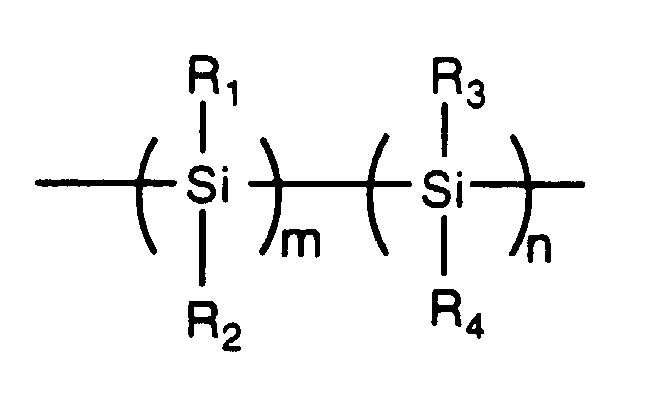
- polysilane which can be used in the present invention
- the number of a carbon atom is 1 to 10, preferably 1 to 6.
- a kind of the substituents R 1 to R 4 and the value of m and n are not particularly important and this polysilane resin may have organic solvent-solubility and can be coated to form an uniform film (film thickness of 0.1 to 10 ⁇ m).
- a photoradical generator is used in the present invention which is a compound generating a halogen radical by light irradiation.
- the present inventors has noticed that a Si-Si bond is cut efficiently by the halogen radical, and the photoradical generator is added in the photosensitive resin composition of the present invention so as to increase the sensitiveness of polysilane to light.
- oxygen is easily inserted into the Si-Si bond, and a synergistic effect can be obtained by an interaction between the photoradical generator and the oxygen supply source. Therefore, it is possible to improve the sensitiveness of polysilane to photodegradation.
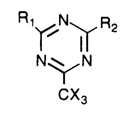
- the photoradical generator may be any compound which generates a halogen radical by light irradiation and is not specifically limited. Examples thereof include 2,4,6-tris(trihalomethyl)-1,3,5-triazine represented by the formula: [wherein X is Cl or Br], 2-substituted-4,6-bis(trihalomethyl)-1,3,5-triazine represented by the formula: [wherein X is Cl or Br, and R is a substituted or non-substituted aliphatic hydrocarbon group, an alicyclic hydrocarbon group and an aromatic hydrocarbon group], 2,4-substituted-6-trihalomethyl-1,3,5-triazine represented by the formula: [wherein X is Cl or Br, and R 1 and R 2 independently indicate a substituted or non-substituted aliphatic hydrocarbon group, an alicyclic hydrocarbon group and an aromatic hydrocarbon group] and the like.
- the oxygen supply source is not specifically limited. Examples thereof include peroxide (e.g. 3,3'4,4'-tetra-(t-butylperoxycarbonyl) benzophenone), amine oxide (e.g. trimethylamine oxide), phosphine oxide (e.g. triphenylphosphine oxide) and the like.
- peroxide e.g. 3,3'4,4'-tetra-(t-butylperoxycarbonyl) benzophenone
- amine oxide e.g. trimethylamine oxide
- phosphine oxide e.g. triphenylphosphine oxide
- the resulting photosensitive resin composition can be put to practical use. Further, by adding a suitable photosensitive dye in addition to the photoradical generator and oxygen supply source, the halogen radical can also be generated due to photoexcitation of the dye.
- the optimum composition of the present invention comprises 1 to 30 parts by weight of the photoradical generator, 1 to 30 parts by weight of the oxygen supply source and 1 to 20 parts by weight of the dye are formulated based on 100 parts by weight of polysilane.
- the dye to be used for example, various soluble dyes, such as coumarin dye, cyanine dye, merocyanine dye are effective.
- a photosensitive layer of the photosensitive resin composition of the present invention is firstly formed on a suitable substrate.
- the substrate its shape and material is not specifically limited. Glass plate, metal plate, plastic plate, can be used according to the application.
- the photosensitive layer is formed on such a substrate.
- a formation method may be any method capable of forming a photosensitive layer having an uniform thickness, and is not specifically limited.
- the above polysilane, photoradical generator and oxygen supply source and, if necessary, dye are dissolved in a solvent capable of dissolving the respective components, such as toluene, THF, to give a solution and the solution can be applied using a spin coater.
- the concentration of the solution is suitably 5 to 15%. It is preferred the dry film thickness of the photosensitive layer is within a range from 0.1 to 10 ⁇ m.
- FIG. 1 (a) to (d) One embodiment of the steps of forming a thin film pattern is shown in Figs. 1 (a) to (d).
- ultraviolet light is irradiated to a laminate 104 for forming pattern thin film comprising a substrate 101 and a photosensitive layer 102, using an ultraviolet light source such as mercury vapor lamp according to the pattern.
- Ultraviolet light or visible light 110 is normally irradiated through a pattern mask 103 put on the laminate 104 for forming thin film.
- the light source used in the present invention has a wavelength wherein the photoradical generator or photosensitive dye is exposed.
- irradiation may be conducted at a light volume of 0.2 to 5 J/cm 2 per 1 ⁇ m in thickness of the photosensitive layer.
- Si-Si bond which exists in the photosensitive layer is cut by light irradiation to form Si-OH (silanol group). Accordingly, a latent image containing a silanol group is formed in the irradiated laminate for forming thin film according to the pattern.
- a sol was absorbed at the pattern part of the laminate for forming thin film.
- water-soluble organic solvents such as acetonitrile, dioxane, tetrahydrofuran, etc. may be added to the metal oxide sol, if necessary,
- a water-soluble organic solvent may be formulated in the sol solution in an amount of 1 to 30% by weight.
- absorption of the sol is suitably conducted by dipping a thin film-forming material in the sol solution maintained at 20 to 40°C for 1 to 40 minutes.
- the material of the metal oxide sol there can be normally used materials used in a sol-gel process.
- the kind of the metal varies depending on the objective function, but examples of the material include metal organic substances (e.g. alkoxide, acetylacetonate, acetate, amine, etc.), soluble inorganic salts (e.g. nitrate, etc.) or dispersants of fine oxide particles of metals (e.g. Si, Zr, Pb, Ti, Ba, Sr, Nb, K, Li, Ta, In, Sn, Zn, Y, Cu, Ca, Mn, Fe, Co, La, Al, Mg, V, etc.).
- metal organic substances e.g. alkoxide, acetylacetonate, acetate, amine, etc.
- soluble inorganic salts e.g. nitrate, etc.
- dispersants of fine oxide particles of metals e.g. Si, Zr, Pb, Ti, Ba, Sr
- a solution which is solated by subjecting to the condensation polymerization reaction using a catalyst such as acid or base.
- a catalyst such as acid or base.
- all substituents of the metal may not be converted into a condensation-polymerizable functional group, but a part of an organic functional group may be remained. Further, materials which can dissolve or disperse in the sol solution may be added.
- tetraethoxysilane is hydrolyzed and condensed with dehydrating by dissolving it in a mixed solution of ethanol and water and adding hydrochloric acid to the mixture, followed by stirring at room temperature for 2 hours to give a homogeneous silica sol.
- composition of the silica sol is preferably composed of 50 to 200 parts by weight of ethanol, 1 to 200 parts by weight of water and 0.1 to 3 parts by weight of hydrochloric acid, based on 100 parts by weight of tetraethoxysilane. If necessary, water-soluble organic solvents such as acetonitrile, dioxane, tetrahydrofuran (THF), etc. may be further added.
- water-soluble organic solvents such as acetonitrile, dioxane, tetrahydrofuran (THF), etc. may be further added.
- the metal oxide sol is absorbed at the ultraviolet light-irradiated part of the photosensitive layer and incorporated into the interior of the photosensitive layer. It is considered that absorption proceeds into the interior through a fine hole which exists in the ultraviolet light-irradiated part of the photosensitive layer.
- the diameter of sol particles is several nm to several tens nm and they can be sticked with diffusing. It was confirmed that a particulate material having a suitable size which coexists with sol particles can be diffused together with sol particles into the interior, similar to the case that sol particles exist alone.
- Examples of the functional atom include fluorine and the like. Water repellency due to fluorine can be imparted on the photosensitive layer by forming a sol containing a lot of fluorine atoms and absorbing the sol on the photosensitive layer.
- Examples of the functional group used in such a method include hydrophobic groups (e.g. alkyl group, etc.), ion-exchange groups (e.g. carboxyl group, sulfo group, acidic hydroxyl group, amino group, etc.) and the like.
- the particulate material examples include copper and silver particles.
- copper and silver particles By preparing a sol in which these particulate materials are coexisted and absorbing the sol and sol particles in the photosensitive layer, copper and silver can be contained in the photosensitive layer as the pattern.
- the particulate material When using a silica sol, the particulate material may be dispersed using the silica sol, or the particulate material may be once dispersed using a nonionic surfactant and then mixed when the silica sol is prepared. In this case, it is necessary to adjust the particle size of the particulate material to not more than 500 nm, preferably not more than 200 nm. When the particle size exceeds 500 nm, particles can not be diffused into the ultraviolet light-irradiated part of photosensitive layer even if they are dipped in the sol solution and, therefore, they can not be sticked. The particle size can be measured by a normal centrifugal sedimentation method. It is considered that silica sol particles are adsorbed on the surface of the particulate material.
- Adsorption of the silica sol on the surface of particles can be easily confirmed by measuring a zeta potential.
- the zeta potential of the material which was dispersed using the nonionic surfactant is dispersed becomes stable at -5 to -25 mV because the silanol group came into existence on the surface by absorption of the silica sol.
- the material which can dissolve in the sol solution may be any material which dissolves in water or alcohol and which interacts with the silanol group of the silica sol, and it can be diffused into the ultraviolet light-irradiated part of the photosensitive layer together with sol particles and sticked.
- Suitable examples of the polymer material include polymers containing an alcoholic hydroxyl group (e.g. polyvinyl alcohol, polyethylene glycol, cellulose, etc.), polymers containing an amide group (e.g. poly(2-methyl-2-oxazoline, poly(N-vinylpyrrolidone), poly(N,N-dimethylacrylamide, etc.) and the like.
- the laminate for forming thin film in which a sol was adsorbed at the pattern part is dried after the sol solution was removed.
- a method of removing the sol solution there can be used a method of washing with water or a method of blowing off by an air blow.
- drying is conducted at more than 100°C for 30 minutes to 2 hours.
- an organic substituent is eliminated by heating at not less than 400°C to give a metal oxide thin film.
- a laminate 104 ' for forming thin film in which a desired pattern is formed By a thin film pattern-forming step, as shown in Fig. 1(b), a laminate 104 ' for forming thin film in which a desired pattern is formed.
- an uneven pattern thin film as shown in Fig. 1 (d) can be obtained by exposing the total surface to ultraviolet light as shown in Fig. 1(c) and decomposing the residual photosensitive layer to remove.
- a method of removing an unnecessary photosensitive layer there can be used a method of volatilizing by heating and a method of removing with a solvent.
- the photosensitive layer is removed by heating, it is sufficient to heat at not less than 200°C for 10 to 60 minutes. In this case, sol particles may have no functional characteristics.
- a thin film having a different function can be easily patterned on the same substrate by changing the part to be exposed to ultraviolet light and repeating the steps of Figs. 1(a) and (b) using a sol solution of a different formulation.
- a photolithography step using a resist which is necessary for patterning is not required in the method for forming a thin film pattern of the present invention.
- a pattern thin film formed by this method can be selected according to the required function because it can form a flat layer having no uneveness unless the photosensitive layer of the non-exposed part is removed, or it can form a pattern thin film having uneveness if the photosensitive layer of the non-exposed part is removed.
- the patterning can form a fine pattern thin film having resolution of "submicron order" because of high resolution of photocomposition of the photosensitive layer, so that, it is suitable for processing of the uneven surface having high density in comparison with a stamper method.
- the applicable area of this technique is wide and a thin film patterning having various functions can be made by selecting the kind of the substrate and material of sol.
- a photosensitive resin composition wherein a sensitiveness of polysilane to photodegradation is improved and a time required for photodegradation is short, and a method for forming a pattern using the same.
- Example 1 According to the same manner as that described in Example 1 except for using 100 parts by weight of the same polysilane as that of Example 1, 10 parts by weight of TAZ-110 and 10 parts by weight of triphenylphosphine oxide (TPPO, manufactured by Tokyo Chemical Industriy Co., LTd.), a sensitiveness was measured. The results are shown in Table 1.
- TPPO triphenylphosphine oxide
- Example 1 According to the same manner as that described in Example 1 except for using only 100 parts by weight of the same polysilane as that of Example 1, a sensitiveness was measured. The results are shown in Table 1.
- Example 1 According to the same manner as that described in Example 1 except for using 100 parts by weight of the same polysilane as that of Example 1 and 10 or 20 parts by weight of TAZ-110, a sensitiveness was measured. The results are shown in Table 1.
- Example 1 According to the same manner as that described in Example 1 except for using 100 parts by weight of the same polysilane as that of Example 1 and 15 or 30 parts by weight of BTTB or 10 or 20 parts by weight of TPPO, a sensitiveness was measured. The results are shown in Table 1.
- Example 1 100 Parts by weight of the same polysilane as that of Example 1, 10 parts by weight of 2,4,6-tris(trichloromethyl) 1,3,5-triazine (TCMT, manufactured by Midori Kagaku Co., Ltd.), 15 parts by weight of BTTB and 5 parts by weight of coumarin pigment, 3,3'-carbonylbis(7-diethylaminocoumarin) (manufactured by Eastman Kodak Co.) were dissolved in THF to give a 10% THF solution. According to the same manner as that described in Example 1, a sample was prepared using the solution.
- TCMT 2,4,6-tris(trichloromethyl) 1,3,5-triazine
- BTTB 15 parts by weight of BTTB
- coumarin pigment 3,3'-carbonylbis(7-diethylaminocoumarin) (manufactured by Eastman Kodak Co.)
- a visible light irradiation time at which absorption of ⁇ max of polysilane is reduced to half was taken as a sensitiveness. Visible light irradiation was conducted using an ultra-high pressure mercury lamp (CL-50-200A, 500 w) manufactured by Japan Storage Battery Co., Ltd. and light having a wavelength of less than 440 nm was cut-off with a filter. The results are as shown in Table 2.
- Example 3 According to the same manner as that described in Example 3 except for using 100 parts by weight of the same polysilane as that of Example 1, 10 parts by weight of TCMT and 15 parts by weight of BTTB or 5 parts by weight of the same coumarin pigment as that of Example 3, a sensitiveness was measured. The results are shown in Table 2. Additive (amount based on 100 parts by weight of polysilane) Example No.
- a toluene solution having the same formulation as that of Example 1 was applied on a glass substrate (5 cm x 5 cm x 0.11 cm in thickness) using a spin coater ("PRS-14", manufactured by Dynapart Co.) so that the dry film thickness may become 2 ⁇ m.
- a quartz photomask was put on the resulting laminate for forming thin film pattern, which was exposed to ultraviolet light at a light volume of 0.5 J/cm 2 using an ultrahigh pressure mercury lamp parallel exposure equipment (CL-50-200A, manufactured by Japan Storage Battery Co., Ltd.). After the photomask was removed, the laminate in which a latent image was formed was dipped in a sol obtained in Preparation Example 2 for 5 minutes. After dipping, the laminate was washed with water and dried at 200°C for 30 minutes to give a patterned thin film of a silica gel.
- Example 4 The same operation as that described in Example 4 was conducted using a 10% solution of polysilane in toluene of Preparation Example 1. As a result, a sol was not fixed because a clear latent image was not formed. Therefore, a sufficient uneven pattern could not be obtained.
- Microlith Red 2BWA “Microlith Red 2BWA”
- Microlith Blue 4GWA "Irgalite Green GLN New” (manufactured by Ciba Geigey Co.) were used as a red pigment, a blue pigment and a green pigment, respectively.
- a toluene solution having the same formulation as that of Example 1 was applied on a glass substrate (5 cm x 5 cm x 0.11 cm in thickness) using a spin coater. Then, this wet film was dried to form a photosensitive layer having a thickness of 2 ⁇ m.
- a silver salt negative film in which a transmission pattern for red color filter was formed was put on the resulting filter material, and a laminate thus obtained was exposed to ultraviolet light at a light volume of 0.5 J/cm 2 using an ultrahigh pressure mercury lamp. After the silver salt negative film was removed, the filter material in which a latent image was formed was dipped in a sol solution for red coloring of Preparation Example 3.
- a silver salt negative film in which a transmission pattern for blue color filter was formed was put on the filter material in place of the silver salt negative film in which a transmission pattern for red color filter was formed, and the resulting laminate was exposed to give a latent image. Then, the second coloring was conducted using a sol for blue coloring.
- the third coloring was conducted to give a color filter.
- the resulting filter is highly transparent and contains no color mixture.
- a spectral transmittance of the color filter was measured using MCPD-1000 manufactured by Ohtsuka Electronics Co., Ltd. The results are as follows: R: 3%, G: 6%, B: 4% at maximum absorption wavelength part.
- Example 5 The same operation as that described in Example 5 was conducted using a 10% solution of polysilane in toluene of Preparation Example 1. As a result, a clear latent image was not formed by exposure and, therefore, sufficient coloring could not be obtained even if the filter material was dipped in a sol.
Landscapes
- Physics & Mathematics (AREA)
- General Physics & Mathematics (AREA)
- Spectroscopy & Molecular Physics (AREA)
- Materials For Photolithography (AREA)
- Photosensitive Polymer And Photoresist Processing (AREA)
- Non-Silver Salt Photosensitive Materials And Non-Silver Salt Photography (AREA)
- Compositions Of Macromolecular Compounds (AREA)
- Exposure And Positioning Against Photoresist Photosensitive Materials (AREA)
- Optical Filters (AREA)
- Liquid Crystal (AREA)
- Exposure Of Semiconductors, Excluding Electron Or Ion Beam Exposure (AREA)
Description


| Additive (amount based on 100 parts by weight of polysilane) | ||||
| Example No. | TAZ-110 | BTTB | TPPO | Exposure time (second) |
| Example 1 | 10 | 15 | 0 | 12 |
| Example 2 | 10 | 0 | 10 | 19 |
| Comparative Example 1 | 0 | 0 | 0 | 62 |
| Comparative Example 2 | 10 | 0 | 0 | 50 |
| Comparative Example 3 | 20 | 0 | 0 | 25 |
| Comparative Example 4 | 0 | 15 | 0 | 43 |
| Comparative Example 5 | 0 | 30 | 0 | 42 |
| Comparative Example 6 | 0 | 0 | 10 | 58 |
| Comparative Example 7 | 0 | 0 | 20 | 56 |
| Additive (amount based on 100 parts by weight of polysilane) | ||||
| TCMT | BTTB | Coumarin | Exposure time (second) | |
| Example 3 | 10 | 15 | 5 | 120 |
| Comparative Example 8 | 10 | 15 | 0 | 440 |
| comparative Example 9 | 10 | 0 | 5 | 630 |
Claims (4)
- A photosensitive resin composition comprising:(a) a polysilane having a structure of the formula:[wherein R1, R2, R3 and R4, the same or different, are selected from the group consisting of a substituted or non-substituted aliphatic hydrocarbon group, an alicyclic hydrocarbon group and an aromatic hydrocarbon group, and m and n indicate an integer],
 (b) a compound which generates a halogen radical by light irradiation, and(c) an oxygen supply source.
 - The photosensitive resin composition according to claim 1, which further comprises a photosensitive dye.
- A method for forming a thin film pattern of a metal oxide, which comprises the steps of:forming a photosensitive layer composed of the photosensitive resin composition of claim 1 or claim 2 on a substrate;selectively exposing the photosensitive layer to light according to a pattern to form a patterned latent image; anddipping the photosensitive layer having the latent image in a sol of the metal oxide.
- The method according to claim 3, wherein the sol of the metal oxide contains a dye or a pigment.
Applications Claiming Priority (2)
| Application Number | Priority Date | Filing Date | Title |
|---|---|---|---|
| JP26228793A JP3274918B2 (en) | 1993-10-20 | 1993-10-20 | Polysilane-based photosensitive resin composition and pattern forming method using the same |
| JP262287/93 | 1993-10-20 |
Publications (2)
| Publication Number | Publication Date |
|---|---|
| EP0650093A1 EP0650093A1 (en) | 1995-04-26 |
| EP0650093B1 true EP0650093B1 (en) | 1998-01-28 |
Family
ID=17373693
Family Applications (1)
| Application Number | Title | Priority Date | Filing Date |
|---|---|---|---|
| EP94307644A Expired - Lifetime EP0650093B1 (en) | 1993-10-20 | 1994-10-18 | Polysilane type photosensitive resin composition and method for forming pattern using the same |
Country Status (5)
| Country | Link |
|---|---|
| EP (1) | EP0650093B1 (en) |
| JP (1) | JP3274918B2 (en) |
| KR (1) | KR100367263B1 (en) |
| DE (1) | DE69408260T2 (en) |
| TW (1) | TW417039B (en) |
Families Citing this family (14)
| Publication number | Priority date | Publication date | Assignee | Title |
|---|---|---|---|---|
| KR100245180B1 (en) * | 1996-05-29 | 2000-02-15 | 니시무로 타이죠 | Photosensitive composition and pattern formation method using the same |
| US5955192A (en) * | 1996-11-20 | 1999-09-21 | Shin-Etsu Chemical Co., Ltd. | Conductive circuit board and method for making |
| JP3301370B2 (en) * | 1997-12-11 | 2002-07-15 | 信越化学工業株式会社 | Method for manufacturing polysilane pattern-formed substrate |
| JP3410968B2 (en) * | 1998-06-22 | 2003-05-26 | 株式会社東芝 | Pattern forming method and photosensitive composition |
| JP3539234B2 (en) * | 1998-10-22 | 2004-07-07 | 信越化学工業株式会社 | Polysilane composition for forming metal pattern coating and metal pattern forming method |
| JP4017795B2 (en) * | 1999-08-27 | 2007-12-05 | 富士フイルム株式会社 | Optical wavelength conversion element and manufacturing method thereof |
| JP4775834B2 (en) | 2002-08-05 | 2011-09-21 | 東京エレクトロン株式会社 | Etching method |
| JP3910908B2 (en) * | 2002-10-29 | 2007-04-25 | 新光電気工業株式会社 | Semiconductor device substrate, manufacturing method thereof, and semiconductor device |
| JP3910907B2 (en) * | 2002-10-29 | 2007-04-25 | 新光電気工業株式会社 | Capacitor element and manufacturing method thereof, substrate for semiconductor device, and semiconductor device |
| JP4493906B2 (en) * | 2002-11-12 | 2010-06-30 | 富士通株式会社 | Liquid crystal display device and manufacturing method thereof |
| US10667340B2 (en) | 2015-01-29 | 2020-05-26 | Dsgi Technologies, Inc. | Microwave assisted parallel plate E-field applicator |
| US11106132B2 (en) * | 2018-04-27 | 2021-08-31 | Tokyo Ohka Kogyo Co., Ltd. | Energy-sensitive composition, cured product, and pattern forming method |
| CN112859520A (en) * | 2021-01-20 | 2021-05-28 | 深圳市撒比斯科技有限公司 | Low-energy-curing photoresist, resist pattern and preparation method thereof |
| KR102702360B1 (en) * | 2023-08-07 | 2024-09-02 | (주)딘에어코리아 | Air cleaner having humidifying function |
Family Cites Families (4)
| Publication number | Priority date | Publication date | Assignee | Title |
|---|---|---|---|---|
| US4588801A (en) * | 1984-04-05 | 1986-05-13 | The United States Of America As Represented By The United States Department Of Energy | Polysilane positive photoresist materials and methods for their use |
| US4820788A (en) * | 1986-10-31 | 1989-04-11 | John M. Zeigler | Poly(silyl silane)homo and copolymers |
| JPH0643655A (en) * | 1991-03-04 | 1994-02-18 | Internatl Business Mach Corp <Ibm> | Forming process of resist image and electronic device |
| KR950002875B1 (en) * | 1991-07-08 | 1995-03-27 | 가부시키가이샤 도시바 | Photosensitive composition |
-
1993
- 1993-10-20 JP JP26228793A patent/JP3274918B2/en not_active Expired - Fee Related
-
1994
- 1994-10-18 DE DE69408260T patent/DE69408260T2/en not_active Expired - Lifetime
- 1994-10-18 EP EP94307644A patent/EP0650093B1/en not_active Expired - Lifetime
- 1994-10-19 KR KR1019940026701A patent/KR100367263B1/en not_active Expired - Fee Related
- 1994-10-22 TW TW083109813A patent/TW417039B/en not_active IP Right Cessation
Also Published As
| Publication number | Publication date |
|---|---|
| JPH07114188A (en) | 1995-05-02 |
| TW417039B (en) | 2001-01-01 |
| KR100367263B1 (en) | 2003-03-19 |
| EP0650093A1 (en) | 1995-04-26 |
| DE69408260D1 (en) | 1998-03-05 |
| JP3274918B2 (en) | 2002-04-15 |
| KR950012154A (en) | 1995-05-16 |
| DE69408260T2 (en) | 1998-05-20 |
Similar Documents
| Publication | Publication Date | Title |
|---|---|---|
| EP0725315B1 (en) | Photosensitive resin composition and method for forming pattern using the same | |
| US5776764A (en) | Polysilane type photosensitive resin composition and method for forming pattern using the same | |
| JP3004044B2 (en) | Photosensitive colored resin composition | |
| EP0650093A1 (en) | Polysilane type photosensitive resin composition and method for forming pattern using the same | |
| EP0654712B1 (en) | Method for forming thin film pattern | |
| EP1043627B1 (en) | Recording material having a pigment-colored radiation-sensitive layer | |
| EP0713144B1 (en) | Photosensitive resin composition | |
| CA1326579C (en) | Ternary photoinitiator system for addition polymerization | |
| JPS58187926A (en) | Method for developing radiation sensitive negative type resist | |
| KR0155990B1 (en) | Photosensitive composition comprising selected photoactive materials and their use in producing high resolution photoresist images with near uv | |
| KR20080067816A (en) | Photosensitive resin composition for black matrices and black matrices prepared therefrom | |
| JP3374380B2 (en) | Cross-linkable high-resolution photoresist composition that can be used with a high base aqueous solution developer and method of forming a photoresist pattern using the composition | |
| JPH10253815A (en) | Photopolymerizable composition for color filter and color filter | |
| JPS58121033A (en) | Photosensitive composition | |
| JP2000003047A (en) | Photosensitive resin composition and pattern forming method using the same | |
| JP2937208B2 (en) | Color filter and manufacturing method thereof | |
| JPS60238829A (en) | Formation of pattern | |
| KR20160115442A (en) | Colored photosensitive resin composition | |
| EP0277555B1 (en) | Copolymers with 0-nitrocarbinol ester groups, and process for preparing two-layer resists and semiconductor devices | |
| JP3956424B2 (en) | Radiation sensitive composition for color filter | |
| JPS61248038A (en) | Method of lowering viscosity for coating for manufacture of photosensitive copying material | |
| US5866306A (en) | Process for use of photosensitive polysilanes as photoresist | |
| KR20160115443A (en) | Colored photosensitive resin composition | |
| KR102918363B1 (en) | A colored photosensitive resin composition, a color filter manufactured from thereof and a solid state pickup device or a display device comprising the same | |
| US20020068234A1 (en) | Recording material having a pigment-coloured radiation-sensitive layer |
Legal Events
| Date | Code | Title | Description |
|---|---|---|---|
| PUAI | Public reference made under article 153(3) epc to a published international application that has entered the european phase |
Free format text: ORIGINAL CODE: 0009012 |
|
| AK | Designated contracting states |
Kind code of ref document: A1 Designated state(s): DE FR GB NL |
|
| 17P | Request for examination filed |
Effective date: 19951013 |
|
| 17Q | First examination report despatched |
Effective date: 19960429 |
|
| GRAG | Despatch of communication of intention to grant |
Free format text: ORIGINAL CODE: EPIDOS AGRA |
|
| GRAG | Despatch of communication of intention to grant |
Free format text: ORIGINAL CODE: EPIDOS AGRA |
|
| GRAH | Despatch of communication of intention to grant a patent |
Free format text: ORIGINAL CODE: EPIDOS IGRA |
|
| GRAH | Despatch of communication of intention to grant a patent |
Free format text: ORIGINAL CODE: EPIDOS IGRA |
|
| GRAA | (expected) grant |
Free format text: ORIGINAL CODE: 0009210 |
|
| AK | Designated contracting states |
Kind code of ref document: B1 Designated state(s): DE FR GB NL |
|
| PG25 | Lapsed in a contracting state [announced via postgrant information from national office to epo] |
Ref country code: FR Free format text: LAPSE BECAUSE OF FAILURE TO SUBMIT A TRANSLATION OF THE DESCRIPTION OR TO PAY THE FEE WITHIN THE PRESCRIBED TIME-LIMIT Effective date: 19980128 |
|
| REF | Corresponds to: |
Ref document number: 69408260 Country of ref document: DE Date of ref document: 19980305 |
|
| EN | Fr: translation not filed | ||
| PG25 | Lapsed in a contracting state [announced via postgrant information from national office to epo] |
Ref country code: GB Free format text: LAPSE BECAUSE OF NON-PAYMENT OF DUE FEES Effective date: 19981018 |
|
| PLBE | No opposition filed within time limit |
Free format text: ORIGINAL CODE: 0009261 |
|
| STAA | Information on the status of an ep patent application or granted ep patent |
Free format text: STATUS: NO OPPOSITION FILED WITHIN TIME LIMIT |
|
| 26N | No opposition filed | ||
| GBPC | Gb: european patent ceased through non-payment of renewal fee |
Effective date: 19981018 |
|
| PGFP | Annual fee paid to national office [announced via postgrant information from national office to epo] |
Ref country code: NL Payment date: 20041003 Year of fee payment: 11 |
|
| PG25 | Lapsed in a contracting state [announced via postgrant information from national office to epo] |
Ref country code: NL Free format text: LAPSE BECAUSE OF NON-PAYMENT OF DUE FEES Effective date: 20060501 |
|
| NLV4 | Nl: lapsed or anulled due to non-payment of the annual fee |
Effective date: 20060501 |
|
| PGFP | Annual fee paid to national office [announced via postgrant information from national office to epo] |
Ref country code: DE Payment date: 20101013 Year of fee payment: 17 |
|
| PG25 | Lapsed in a contracting state [announced via postgrant information from national office to epo] |
Ref country code: DE Free format text: LAPSE BECAUSE OF NON-PAYMENT OF DUE FEES Effective date: 20130501 |
|
| REG | Reference to a national code |
Ref country code: DE Ref legal event code: R119 Ref document number: 69408260 Country of ref document: DE Effective date: 20130501 |