EP0649230B1 - Modulateur numérique à débit variable et son utilisation en radiodiffusion FM - Google Patents
Modulateur numérique à débit variable et son utilisation en radiodiffusion FM Download PDFInfo
- Publication number
- EP0649230B1 EP0649230B1 EP94402310A EP94402310A EP0649230B1 EP 0649230 B1 EP0649230 B1 EP 0649230B1 EP 94402310 A EP94402310 A EP 94402310A EP 94402310 A EP94402310 A EP 94402310A EP 0649230 B1 EP0649230 B1 EP 0649230B1
- Authority
- EP
- European Patent Office
- Prior art keywords
- signal
- modulation
- type
- frequency
- digital
- Prior art date
- Legal status (The legal status is an assumption and is not a legal conclusion. Google has not performed a legal analysis and makes no representation as to the accuracy of the status listed.)
- Expired - Lifetime
Links
Images



Classifications
-
- H—ELECTRICITY
- H04—ELECTRIC COMMUNICATION TECHNIQUE
- H04H—BROADCAST COMMUNICATION
- H04H20/00—Arrangements for broadcast or for distribution combined with broadcast
- H04H20/28—Arrangements for simultaneous broadcast of plural pieces of information
- H04H20/33—Arrangements for simultaneous broadcast of plural pieces of information by plural channels
- H04H20/34—Arrangements for simultaneous broadcast of plural pieces of information by plural channels using an out-of-band subcarrier signal
-
- H—ELECTRICITY
- H04—ELECTRIC COMMUNICATION TECHNIQUE
- H04L—TRANSMISSION OF DIGITAL INFORMATION, e.g. TELEGRAPHIC COMMUNICATION
- H04L27/00—Modulated-carrier systems
- H04L27/18—Phase-modulated carrier systems, i.e. using phase-shift keying
-
- H—ELECTRICITY
- H04—ELECTRIC COMMUNICATION TECHNIQUE
- H04H—BROADCAST COMMUNICATION
- H04H2201/00—Aspects of broadcast communication
- H04H2201/10—Aspects of broadcast communication characterised by the type of broadcast system
- H04H2201/13—Aspects of broadcast communication characterised by the type of broadcast system radio data system/radio broadcast data system [RDS/RBDS]
Definitions
- the invention relates to a digital flow modulator variable, and its use in modulation broadcasting frequency, designated by FM broadcasting.
- the FM broadcasting system allows, in addition to broadcasting frequency modulation radio programs, the transmission of information or service data intended car radio, messaging or remote display users.
- the system used in these countries is the RDS system (Radio Data System).
- This system consists, as shown in FIG. 1 in the case of a stereophonic emission, to be introduced into the spectrum of the baseband signal FM multiplex a frequency-centered subcarrier 57 kHz center, with an occupied frequency band ⁇ 2.375 kHz around the above-mentioned center frequency.
- the wave the aforementioned subcarrier in RDS channel ensures the transmission of service data, with a low speed of around 1,200b / s.
- the low value of the transmission rate of the RDS channel does not allow the broadcasting of new services such as broadcasting still images or news journals.
- one approach may be to generate, in addition to the RDS channel, an additional channel, consisting of example in an additional subcarrier allowing the transmission of additional data or information.
- an additional channel consisting of example in an additional subcarrier allowing the transmission of additional data or information.
- the signal baseband consists of all of the audio signals and additional signals.
- CCIR recommendation 450-1 (Advisory Committee International Radiocommunications), relating to standards frequency in VHF, specifies that the frequency central of any additional data subcarrier must be between 15 and 23 kHz or 53 and 76 kHz, without however specify the maximum width of the band signal multiplex base.
- the N.H.K. is likely to contribute to the emission of a frequency modulated signal may cause interference with channels adjacent, especially in Europe and France, countries in which the spacing between two channels is 100 kHz. A direct use of the two aforementioned systems is therefore not hardly possible.
- the object of the present invention is to remedy the disadvantages mentioned above by the use of a modulator digital variable speed, allowing the promotion of new services in FM broadcasting, by introduction an additional data transmission channel fully compatible with both recommendation 450-1 than with the aforementioned 1,065 CCIR report.
- Another object of the present invention is the implementation using a digital variable rate modulator allowing switching between two flow values of additional data transmitted, depending on the applications or services performed, during the transmission of these additional data.
- Another object of the present invention is further the implementation of a digital modulator with a flow of switchable transmission, without changing the width of signal band modulated around a carrier wave similarly center frequency.
- Another object of the present invention is finally the implementation of a variable rate digital modulator authorizing the promotion of new broadcasting services FM, fully compatible with the R.D.S. system of transmission of auxiliary data.
- the digital modulator with variable signal flow digital emission, object of the present invention is remarkable in that it includes a demultiplexing circuit time of this digital broadcast signal in one first and a second elementary transmission signal, and first and second emission filtering circuits in baseband corresponding to a first type of modulation at a first rate and at a second type of modulation at a second flow respectively.
- the first and the second baseband emission filtering circuit receive the first respectively the second transmission signal elementary and deliver a first respectively a second elementary signal filtered.
- a control circuit flow switching, by switching from first to second filtering mode, or vice versa, from a flow control signal is expected.
- a modulator circuit in phase and in quadrature of phase of a carrier wave of determined frequency fo receives on its modulation inputs the first respectively the second elementary signal filtered and delivers a first respectively a second modulated carrier signal and an adder circuit receiving the first and second carrier signals modulated provides a modulated carrier signal resulting.
- a filter circuit centered on the frequency fo of the carrier wave eliminates the periodicity of the spectrum of the resulting modulated carrier signal, for deliver a resultant modulated signal filtered for broadcast.
- variable rate digital modulator object of the present invention finds application in the implementation FM broadcast transmitters, for the transmission of additional data to the auxiliary data of type R.D.S., with a view to promoting new services put at the available to users or listeners.
- the signal emission denoted e (t)
- e (t) is formed by a sequence of bits of any representative value of the information or additional data to be transmitted in FM broadcasting.
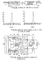
- the modulator object of the present invention comprises a digital signal temporal demultiplexing circuit 1 emission e (t) in a first e1 (t) and in a second e2 (t) elementary emission signal, each also constituted by a series of bits. It is thus understood that for a signal digital transmission e (t) at a bit frequency formed by a square wave signal Fb, actually corresponds, due demultiplexing, a symbol frequency Fs equal to the half the frequency bits, symbols or groups of symbols of course being at least partially representative additional information to be transmitted.
- the digital modulator object of the present invention comprises also a module 2 for band emission filtering basis of the first and second elementary transmission signals e1 (t), e2 (t).
- the band filter emission module 2 base actually has a first and a second circuit baseband emission filtering noted 21 respectively 22, these circuits making it possible to carry out a first type of modulation at a first rate respectively a second type of modulation at a second rate, the first and the second elementary emission signal e1 (t), e2 (t).
- the first 21 and second 22 emission filter circuit in baseband receiving the first respectively the second elementary emission signal deliver a first respectively a second filtered elementary signal, noted e1f (t), e2f (t).
- the baseband emission filtering module 2 includes a flow control input receiving a corresponding signal, denoted cde, this signal making it possible to ensure switching from the first flow to the second flow or vice versa, by switching from the first type of modulation to second type of modulation or vice versa, as well as will be described below in the description.
- the modulator object of this invention includes a modulator circuit in phase and in phase quadrature of an additional subcarrier wave, more conveniently designated by carrier wave, frequency fO, receiving on its modulation inputs the first respectively the second filtered elementary signal e1f (t), e2f (t) and delivering a first respectively a second modulated carrier signal, these signals being denoted spm1, spm2 in Figure 2a.
- the modulator 3 includes, so conventional, a first and a second modulator circuit 31, 32 supplied by the carrier wave in phase respectively phase quadrature by an oscillator 30 at the frequency f0.
- an adder circuit 4 is provided which receives the first and the second spm1 modulated carrier signal, spm2 and outputs a resultant modulated carrier signal noted spmr.
- a filtering circuit centered on the frequency of the carrier wave f0, this circuit being noted 5 on the FIG. 2a, makes it possible to eliminate the periodicity of the spectrum of the resulting modulated carrier signal spmr to deliver a filtered filtered modulated signal intended for broadcasting.
- variable rate digital modulator object of the present invention can thus be controlled in flow by the flow control signal, denoted cde, which, via the flow switching circuit 20 , ensures the choice of the first filtering mode respectively of the second filtering mode of the first and of the second baseband transmission filtering circuit 21 and 22, that is to say finally, by the choice of the corresponding transfer function denoted He1 1 (f) and He1 2 (f) of the first and second filtering circuits 21 and 22, to make the choice of the flow rate associated with the corresponding filtering mode, as will be described later in the description.
- the flow control signal denoted cde
- the first and second filter circuits baseband transmission 21, 22 may include successively in cascade a digital synthesis module of a waveform receiving the first, respectively the second elementary emission signal e1 (t), e2 (t).
- a digital synthesis module of a waveform receiving the first, respectively the second elementary emission signal e1 (t), e2 (t).
- the digital source or emission signal e (t) is demultiplexed to form the first and second aforementioned elementary emission signal.
- the digital synthesis module allows to generate a suite of samples corresponding to the first respectively to second type of modulation, depending on the choice of modulation and therefore debit retained.
- a digital to analog converter rated DAC on FIG. 2b receives the above-mentioned series of samples and delivers the first respectively the second signal elementary filtered e1f (t), e2f (t).
- Tb designates the duration or the period bits
- the emission filtering according to the transfer function He1 1 (f) or He1 2 (f) is carried out in baseband in digital form, the analog bandpass filtering carried out by filtering 5 at the output of the modulator object of the present invention, having only the function of eliminating the periodicity of the spectrum of the resulting filtered modulated signal but having no role relative to the shaping of this signal.
- the baseband filtering of the digital train consisting of the following symbols [an] transmitted with a rhythm 1 / Ts, with Ts equal to 2Tb, Tb designating the duration or period of the sequence of bits constituting the transmission signal e (t), leads to the filtered signal:
- the first and the second type of modulation used are of course types of modulation compatible with the RDS system.
- the first type of modulation can consist of a type of 1/2 phase modulation modulation modulation can be broken down into quasi-linear and that the second type of modulation used may consist of modulation OQPSK, regardless of the type of filtering used. So the type of GMSK modulation used in the digital second generation GSM radio as well as the type of modulation used in the broadcast system Darc data can be used.
- radiocommunication systems of the future are likely to use several types of modulation as mentioned above. These appear to be well suited to the various transmission media, such as the interior of a building, urban, suburban and rural, and are likely to allow the implementation of coding devices comprising a digital modulator conforming to the object of the present invention.
- Such digital radiocommunication systems have been described in the article " ATDMA System Concept” from the Race Mobile Telecommunications Workshop conference which took place in Metz, France, from June 16 to 18, 1993, and published by HJ EUL, SIEMENS.
- the first type of modulation can for example consist of an OQPRS modulation, the baseband filter of transfer function He1 1 (f) being a filter equivalent to coding duobinary.
- the second type of modulation used corresponding to the transfer function He1 2 (f) is an OQPSK modulation, the baseband filter being a raised cosine filter, the overflow factor of which is designated by ROLL-OFF FACTOR in Anglo-Saxon language is taken equal to 0.5.
- the global filtering thus obtained satisfies the NYQUIST criterion with optimal sharing between transmission and reception, this which ensures the absence of interference between symbols and obtaining ideal theoretical performance in terms of error rate in the presence of Gaussian noise.
- FIG. 2c gives a representation of the impulse response of the shaping filters, that is to say the impulse response associated with the transfer functions He1 1 (f) respectively He1 2 (f) in the case of the OQPSK modulation types. respectively OQPRS.
- the corresponding diagrams are plotted in relative amplitude value on the ordinate axis and as a function of time, the time being identified with respect to the symbol period Ts.
- a corresponding embodiment then allows, for a fixed clock frequency of determined value, to obtain a first type of modulation of the OQPSK type performed at a speed of 19.2 kb / s and a second type of OQPRS type modulation with a bit rate of 30 kb / s for a 15 kHz bandwidth centered on a frequency of the carrier wave close to 68.5 kHz.
- the first possibility is to use a digital signal processor for performing filtering of data by calculation in real time, by a discrete convolution between the received signal and the response impulse shaping filters as shown in Figure 2c.
- This filtering method presents the disadvantage of carrying out a very large number of multiplications / accumulations requiring a cycle time less than 40 ns and therefore resulting in a significant additional cost.
- Another solution can consist in carrying out a data transcoding filtering, which has the advantage to be inexpensive and easy to implement, transcoding operations also having the advantage of require at most read access to a memory of transcoding, which allows direct delivery of the filtered elementary signal e1f (t), e2f (t), as it will be described later in the description.
- the digital modulator with variable flow, object of the present invention comprises associated with the circuit filter 21 and 22 above a shift register, noted 212 respectively 222, each shift register being preceded by a differential encoder noted 211 respectively 221.
- Differential encoder 211 receives the first signal transmission element e1 (t) and the differential encoder 221 receives the second elementary emission signal e2 (t) by via a delay circuit 220, which allows introduce a delay of a bit period Tb on the signal cited above.
- a counter 23 is provided to allow discrimination on L consecutive symbols as well as previously mentioned in the description.
- the configuration L symbols in each shift register 212, 222 by transcoding generates a signal or sequence of N samples, this signal being defined over a symbol period Ts.
- the configuration L symbols in each shift register 212, 222 changes, by shifting a bit from left to right, and at each symbol period Ts a new signal, sequence of N samples of duration Ts is generated, this signal constituting the elementary filtered signal e1f (t), e2f (t).
- the flow switching circuit 20 then makes it possible, from the flow control signal cde to act on the differential encoders 211 and 221 so, ultimately, to inhibit differential coding, i.e. precoding, when the type of modulation chosen corresponds to the first type of OQPSK modulation, and on the contrary to validate the precoding, i.e. the operation of encoders 211 and 221 differentials when the type of modulation chosen is the second type of OQPRS modulation.
- each differential encoder 211 or 221 can be formed by an exclusive OR logic circuit bearing the reference 2110, 2210, one entry of which is closed on the output via a delay circuit 2111, 2211, the delay introduced by this circuit being equal to a duration or period bits Tb.
- the flow switching circuit 20 may consist of example in a logic switch which allows to deliver simply the first elementary emission signal e1 (t) and the second elementary transmission signal e2 (t) delayed a bit period or duration Tb by the delay circuit 220, in the case where the first type of OQPSK modulation was chosen, and on the contrary the previously mentioned signals precoded via the first differential encoder 211 respectively of the second differential encoder 221, when the second type of OQPRS modulation has been chosen. These signals are delivered on a line I and a line Q at shift register 212 respectively 222.
- the impulse responses are obtained as shown in Figure 2c for the corresponding modulation type OQPSK respectively OQPRS by an inverse Fourier transform.
- the aforementioned impulse responses decrease and become negligible for a signal width equivalent to eleven bit periods Tb.
- this consists of filtering by transcoding of values, these values of course stored in a PROM type memory circuit and the PROM filtering being similar to a convolution operation.
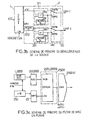
- FIG. 3c shows the filtering circuit 21 consisting of a 2100 EPROM type memory receiving from from demultiplexer 1 the first elementary transmission signal e1 (t) via the shift register 212. In the case of the baseband emission filtering circuit bearing the reference 22, this receives the second signal elementary emission e2 (t) through the circuit delay 220 of a bit period Tb.
- the shift register carries the reference 222 and the circuit of filtering 22 is constituted for example by a memory of type EPROM 2200.
- the demultiplexer 1 delivering the first signal elementary emission signal e1 (t) and the second emission signal elementary e2 (t) through the circuit of delay 220 is represented by the reference 1,220 on the figure 3c.
- the capacity of the EPROM memory corresponds to that of the product of the number of combinations by 32, number of values.
- the counter 23 formed by a 5-stage counter allows addressing thirty-two values for each combination, and the first or second signal elementary filtered e1f (t), e2f (t) is available on a BUS 2100 or 2200 EPROM memory output. indicates that the clock signal at the bit 1 / Tb frequency is multiplied by 32 by a frequency multiplier 230 for address the counter 23.
- the shift register 212 or 222 allows addressing the most significant of the EPROM memory 2100 or 2200 while counter 23 addresses the bits of low memory weight to obtain 32 samples required.
- the first and the second filtered elementary signal are then delivered by the output bus of the EPROM memory 2100, 2200 to the corresponding analog-to-digital converter 213 or 214 to ensure the attack on the modulator circuit 3 by the corresponding analog signals.
- the demultiplexer 1 is not not shown so as not to overload the drawing.
- this embodiment eliminates any necessary precoding operation OQPRS modulation type, the filtering operation being of course performed by pure transcoding of the first and second elementary emission signal e1 (t), e2 (t), i.e. by reading the values stored in a PROM memory unique 2400, these values being representative of the first and the second filtered elementary emission signal e1f (t), e2f (t) above.
- Baseband emission filtering circuits are thus formed by the first shift register 212, the second shift register 222, which are interconnected by a BUS connection to memory 2400 previously mentioned.
- Shift register 212 receives the first elementary signal e1 (t) as well as a timing signal Hs frequency clock symbol. This clock signal allows sample the corresponding symbols.
- Shift register 222 receives second signal elementary emission e2 (t) as well as the clock signal aforementioned symbol, delayed by a period equal to the period symbol Ts.
- Ts 2.Tb.
- Each shift register 212, 222 delivers alternately every two periods of the clock signal HS symbol sampling, a corresponding symbol on the BUS type line interconnected to the PROM memory 2400.
- the aforementioned PROM memory circuit of the type programmable, alternately receives the symbols formed by the eleven bits delivered by each shift register 212 and 222, as well as the flow control signal cde constituted for example by a logic signal representative of the type of modulation and therefore of the chosen bit rate.
- the PROM memory circuit 2400 then delivers, by transcoding, a signal of sign ss and an absolute value signal, denoted sav, these signals being of course representative of the first and second signal elementary filtered.
- the BUS type connection allows for example to transmit bits A0 to A3 relating to the clock signals symbol HS, 2HS, 4HS and 16HS, the eleven bits A4 to A14 representative of the combination delivered by each shift register and bit A15 representative of the signal flow control cde.
- the first and second signal filtered elementary delivered by the PROM 2400 memory is by example delivered coded on 8 bits D0 to D6 relating to the value absolute and bit D7 relative to the sign of each signal.
- the modulator circuit 3 in phase and in quadrature phase can be constituted by a digital modulator comprising two exclusive OR type circuits marked 310 and 320, receiving on a first input the sign signal ss and on a second input a clock signal whose frequency is equal to that of the carrier wave f0.
- the carrier frequency clock signal f0 can be formed by a divider by 4 circuit noted 300, which receives in input a clock signal of frequency 4.f0.
- circuit 300 plays the role of circuit 30 so that circuits 310 and 320 play the role of circuits 31 and 32 respectively in the analog phase modulator and in phase quadrature as shown in FIG. 2a.
- a bit concatenation circuit 40 receives on the one hand the signal delivered by each circuit of exclusive OR type 310, 320, and on the other hand the signal ss sign issued by the PROM 2400 type memory circuit.
- the number N of samples processed by significant symbol is divided by two and reduced from 32 to 16, the basic frequency of the clock signal clk being divided by two and reduced from 15.36 MHz to 7 , 68 MHz, although the bit rates of the first and second types of OQPSK, OQPRS modulation are maintained at the previous values 19.2 kb / s respectively 30 kb / s.
- the capacity of the PROM filtering memory 2100 or 2400 can therefore be divided by two, which makes it possible to use a single PROM memory of the same capacity, instead of two, by means of a multiplexed addressing of the memory PROM 2100 (2400) to starting from the pre-coded signals or not, delivered on a depth of 11 bits by the shift registers 212 or 222, according to the filtering mode selected OQPRS or OQPSK, as described previously in the description. Due to the multiplexed addressing of the PROM memory 2100 or 2400 in the embodiment of FIG. 5a, the data of the digital signal delivered by the above-mentioned shift registers are locked (latched in Anglo-Saxon language).
- the shift registers 212 and 222 are constituted by “latches” flip-flops with three states wired in shift register.
- the clock 6 delivers secondary clock signals at the frequency Fb / 2, Fb, 2Fb, 4Fb, 8Fb and 16Fb, where Fb denotes the bit frequency.
- the secondary clock signals 16Fb, 8Fb control the digital to analog converter 213, which is followed by analog band filters 215, 216, 4Fb, 2Fb, Fb and 8Fb, Fb / 2 signals through an inverter 60 and an exclusive OR gate 61 on PROM 2100 read addressing sequencing or 2400, the signal Fb / 2 the demultiplexer 1, the signal 8Fb, directly by two cascade inverters 60, 2221 and by through inverter 60 shift registers 222 and 221 respectively, the signal Fb / 2 the timing of shift registers 222, 212, via a inverter 2220 and directly respectively.
- the signals delivered by the PROM filtering memory 2100 or 2400 corresponding to the first respectively to the second filtered elementary signal e1f (t), e2f (t) are then directly converted to analog signal by converter digital analog 213, then filtered by filters low pass 215, 216 to deliver the first respectively the second elementary signal filtered in analog form, before transposition.
- FIG. 5b shows the loop at phase lock 7, PLL, which includes a divider frequency by 38 referenced 70 receiving the frequency pilot Fp and delivering a divided pilot signal, an OR gate exclusive 71 performing the phase comparison between the divided pilot signal and a divided local oscillator signal, a low pass loop filter 72 attenuated from the first variable time constant order and potentiometric setup 73 allowing a fraction of the signal to be taken filtered output delivered by filter 72. Potentiometric mounting 73 controls a voltage controlled oscillator 74 which delivers the clock signal clk at base frequency 7.68 MHz by a shaping circuit 75.
- a circuit frequency divider by 15 360 delivers an oscillator signal room divided at exclusive OR gate 71 for comparison phase with the divided pilot signal.
- the local oscillator 74 is a very stable oscillator with stabilized power supply by Zener diodes to obtain a rest frequency too as close as possible to 7.68 MHz, which makes it possible to define a narrow capture range and thereby decrease the jitter phase linked to the significant multiplication factor of the pilot frequency (15,360).
- the clock 7 may include a frequency synthesizer, incorporated or not, in order to frequency control the clock signals auxiliaries issued by the latter. This allows the case if necessary to obtain a first and a second variable flow and adjustable, continuously for example, within a range of flow values proportional to the frequency variation clock signals.
Landscapes
- Engineering & Computer Science (AREA)
- Signal Processing (AREA)
- Computer Networks & Wireless Communication (AREA)
- Digital Transmission Methods That Use Modulated Carrier Waves (AREA)
- Stereo-Broadcasting Methods (AREA)
Description
- le système RECEPTOR développé aux Etats-Unis d'Amérique par la société AT&E. Ce système permet un débit de transmission de données supplémentaires de 19 kb/s par codage duobinaire, puis modulation en amplitude à double bande latérale d'une sous-porteuse de fréquence centrale 66,5 kHz. L'occupation spectrale est de ± 9,5 kHz autour de la fréquence centrale précitée et le spectre du signal du système RECEPTOR est compris dans la bande de fréquences 57-76 kHz. Ce système présente donc l'inconvénient du recouvrement des spectres des signaux des canaux RDS et RECEPTOR, rendant le système RECEPTOR incompatible avec le système RDS, sauf introduction d'un filtrage de la partie basse du spectre RECEPTOR, au prix d'une diminution de performances.
- Le système proposé par la société N.H.K. (Japan Broadcasting Corporation) permet des applications ou prestations de services très diverses telles que télétexte, son numérique, en raison du débit de transmission très important, 48 kb/s. Le système N.H.K. met en oeuvre un processus de modulation de type QPSK, (Quadrature Phase Shift Keying) dans lequel le signal de données est modulé autour d'une sous-porteuse de fréquence centrale 76 kHz. Le spectre du canal N.H.K. situé entre les fréquences 60,4 et 91,6 kHz est compatible avec le système R.D.S. Toutefois la fréquence maximale du signal bande de base multiplex, 91,6 kHz, est largement supérieur à la fréquence maximale en émission 76 kHz, telle que définie par le rapport 1 065 du CCIR, Spectre RF des émetteurs de radiodiffusion sonore à modulation de fréquence, question 46/10, Programme d'étude 46 L/10.
- la figure 2a représente un schéma de principe sous forme de blocs fonctionnels du modulateur numérique à débit variable, objet de la présente invention,
- la figure 2b représente un schéma de principe illustratif du processus de filtrage pour mise en forme du signal d'émission,
- la figure 2c représente la réponse impulsionnelle de filtres de mise en forme du signal d'émission permettant une modulation à un premier respectivement à un deuxième débit de transmission,
- la figure 3a représente un mode de réalisation avantageux du modulateur numérique à débit variable objet de l'invention tel que représenté en figure 2a,
- la figure 3b représente un détail de réalisation de la figure 3a, relatif au démultiplexage des échantillons constitutifs du signal d'émission,
- la figure 3c représente un mode de réalisation particulier des filtres de mise en forme ou filtres d'émission en bande de base correspondant au premier type de modulation à un premier débit respectivement au deuxième type de modulation à un deuxième débit,
- la figure 4 représente un mode de réalisation préférentiel non limitatif du modulateur numérique à débit variable objet de l'invention représenté en figure 3a, 3b et 3c,
- la figure 5a représente le schéma général d'un modulateur asservi sur la fréquence du signal pilote du signal multiplex stéréo,
- la figure 5b représente le schéma d'une boucle à verrouillage de phase.


- le train de bits démultiplexé subit un précodage,
- la réponse du filtre de mise en forme est différente.
- le débit choisi et par conséquent le type de modulation retenu OQPSK ou OQPRS,
- le contenu de l'un des registres à décalage 212 ou 222 lequel représente une combinaison formée par onze symboles de données à filtrer,
- les signaux d'horloge symbole Hs et de bits dont la combinaison représente le rang de l'échantillon parmi les 32 échantillons de chaque symbole.
| Symboles | Fb=2Fs=1/Tb | Ts=2Tb | Fe=16Fs=8Fb |
| Description | Fb : fréquence bit | Ts : période symbole | Fe : fréquence d'échantillonnage |
| Fs : fréquence symbole | Tb : période bit | ||
| OQPSK | 19,2 kbits/s | ≃ 104,17µs | 153,6 kHz |
| OSPRS | 30 kbits/s | ≃ 66,67µs | 240 kHz |
| Fclk=7,68 MHz | Fclk=fréquence de l'oscillateur local |
| Fclk=50*Fe=400*Fb | en OQPSK |
| Fclk=32*Fe=256*Fb | en OQPRS |
| Fclk=112*F0 = 68,571kHz | en OQPSK et OQPRS |
| f0=fréquence le la sous-porteuse supplémentaire ou onde porteuse. |
Claims (10)
- Modulateur numérique à débit variable d'un signal numérique d'émission e(t), caractérisé en ce qu'il comprend :des moyens (1) de démultiplexage temporel dudit signal numérique d'émission e(t) en un premier et un deuxième signal d'émission élémentaire el(t), e2(t),des premiers (21) et deuxièmes (22) moyens de filtrage d'émission en bande de base, chacun desdits moyens de filtrage pouvant fonctionner selon un premier ou un second mode de filtrage, correspondant à un premier type de modulation à un premier débit respectivement à un deuxième type de modulation à un deuxième débit, lesdits premiers (21) et deuxièmes (22) moyens de filtrage d'émission en bande de base recevant le premier el(t) respectivement le deuxième e2(t) signal d'émission élémentaire et délivrant un premier respectivement un deuxième signal élémentaire filtré, elf(t), e2f(t),des moyens (20) de commande de commutation de débit par commutation du premier au deuxième mode de filtrage, ou réciproquement, recevant un signal de commande de débit,des moyens modulateurs (3) en phase et en quadrature de phase d'une onde porteuse de fréquence f0 recevant sur leurs entrées de modulation le premier respectivement le deuxième signal élémentaire filtré et délivrant un premier respectivement un deuxième signal de porteuse modulée,des moyens additionneurs (4) recevant lesdits premier et deuxième signal de porteuse modulée et délivrant un signal de porteuse modulée résultant,des moyens de filtrage (5) centrés sur la fréquence de l'onde porteuse f0 permettant d'éliminer la périodicité du spectre du signal de porteuse modulé résultant pour délivrer un signal modulé résultant filtré, pour diffusion.
- Modulateur selon la revendication 1, caractérisé en ce que lesdits premiers (21) et deuxièmes (22) moyens de filtrage d'émission en bande de base comprennent chacun successivement en cascade :un module (21;22) de synthèse numérique d'une forme d'onde recevant ledit premier respectivement deuxième signal d'émission élémentaire el(t), e2(t), constitutifs chacun d'une suite de symboles, ledit module de synthèse formant filtre en bande de base, permettant d'engendrer une suite d'échantillons correspondant au premier respectivement au deuxième type de modulation,un convertisseur numérique analogique (CNA) recevant ladite suite d'échantillons et délivrant le premier respectivement le deuxième signal élémentaire filtré el(t), e2(t).
- Modulateur selon la revendication 2, caractérisé en ce que le premier type de modulation est une modulation à phase continue d'indice 1/2 de type quasi-linéaire, et en ce que le deuxième type de modulation est une modulation OQPSK.
- Modulateur selon la revendication 3, caractérisé en ce que le premier type de modulation étant une modulation OQPRS le filtre en bande de base est un filtre équivalent au codage duo-binaire, et en ce que le deuxième type de modulation étant une modulation OQPSK le filtre en bande de base est un filtre en cosinus surélevé.
- Modulateur selon la revendication 4, caractérisé en ce que, pour une fréquence d'horloge fixe de valeur déterminée, le premier et le deuxième type de modulation sont réalisés à un débit de 30 kb/s respectivement 19,2 kb/s pour une largeur de bande de 15 kHz centrée sur une fréquence de l'onde porteuse f0 voisine de 68,5 kHz.
- Modulateur selon l'une des revendications 1 à 5, caractérisé en ce que lesdits premier (21) et deuxième (22) moyens de filtrage comportent :un registre à décalage (212;222) recevant ledit premier respectivement deuxième signal d'émission ainsi qu'un signal d'échantillonnage de symboles direct respectivement retardé d'une période T de la période du signal d'échantillonnage de symboles, chaque registre à décalage (212;222) délivrant alternativement toutes les deux périodes du signal d'horloge d'échantillonnage de symboles un symbole correspondant,un circuit mémoire (2400) de type programmable PROM, recevant alternativement lesdits symboles ainsi qu'une variable représentative du type de modulation et de débit choisi, et délivrant par transcodage un signal de signe et un signal de valeur absolue représentatifs du premier et du deuxième signal élémentaire filtré.
- Modulateur selon les revendications 1 et 6, caractérisé en ce que lesdits moyens modulateurs en phase et en quadrature de phase sont formés par un modulateur numérique comprenant :deux circuits de type OU exclusif (310, 320) recevant chacun sur une première entrée ledit signal de signe et sur une deuxième entrée un signal d'horloge (300) dont la fréquence est égale à celle de l'onde porteuse f0,un circuit (40) de concaténation de bits recevant d'une part le signal délivré par chaque circuit de type OU exclusif et, d'autre part, le signal de signe délivré par ledit circuit mémoire de type PROM, et délivrant sous forme numérique ledit signal d'émission modulé,un circuit convertisseur numérique analogique (41) recevant ledit signal d'émission modulé sous forme numérique et délivrant un signal d'émission analogique correspondant.
- Modulateur selon l'une des revendications précédentes, caractérisé en ce que lesdits premier (21) et deuxième (22) moyens de filtrage sont asservis sur la fréquence pilote Fp = 19kHz du signal multiplex stéréo, par l'intermédiaire d'une boucle à verrouillage de phase (7) et d'une horloge (6), ce qui permet d'asservir les débits des premier et deuxième type de modulation et la fréquence du signal de porteuse modulée résultant à ladite fréquence pilote.
- Modulateur selon la revendication 8, caractérisé en ce que ladite horloge (6) comporte un synthétiseur de fréquences, ce qui permet de commander en fréquence les signaux d'horloge délivrés par ladite horloge (6) pour obtenir un premier et un deuxième débit variable et ajustable dans une plage de valeurs de débits proportionnelle à la variation de fréquence des signaux d'horloge.
- Utilisation d'un modulateur selon l'une des revendications précédentes pour la transmission d'informations supplémentaires en radiodiffusion FM.
Applications Claiming Priority (2)
| Application Number | Priority Date | Filing Date | Title |
|---|---|---|---|
| FR9312436 | 1993-10-19 | ||
| FR9312436A FR2711464B1 (fr) | 1993-10-19 | 1993-10-19 | Modulateur numérique à débit variable et son utilisation en radiodiffusion FM. |
Publications (2)
| Publication Number | Publication Date |
|---|---|
| EP0649230A1 EP0649230A1 (fr) | 1995-04-19 |
| EP0649230B1 true EP0649230B1 (fr) | 2001-04-04 |
Family
ID=9451981
Family Applications (1)
| Application Number | Title | Priority Date | Filing Date |
|---|---|---|---|
| EP94402310A Expired - Lifetime EP0649230B1 (fr) | 1993-10-19 | 1994-10-14 | Modulateur numérique à débit variable et son utilisation en radiodiffusion FM |
Country Status (6)
| Country | Link |
|---|---|
| US (1) | US5473290A (fr) |
| EP (1) | EP0649230B1 (fr) |
| JP (1) | JPH07254886A (fr) |
| DE (1) | DE69427009D1 (fr) |
| FI (1) | FI944882A7 (fr) |
| FR (1) | FR2711464B1 (fr) |
Families Citing this family (10)
| Publication number | Priority date | Publication date | Assignee | Title |
|---|---|---|---|---|
| JP3463828B2 (ja) * | 1994-11-21 | 2003-11-05 | ソニー株式会社 | 送信機 |
| US5591931A (en) * | 1995-01-17 | 1997-01-07 | Virtual Dsp Corporation | Musical signal multiplexing circuit and demultiplexing system |
| US5630103A (en) * | 1995-03-20 | 1997-05-13 | Smith; Patrick C. | Radio transmission system for distribution of newspaper copy in computer format to personal computers for viewing |
| US6160838A (en) * | 1996-12-13 | 2000-12-12 | Uniden Corporation | Spread spectrum transmitter, spread spectrum receiver and spread spectrum communication method and automatic gain control circuit for spread spectrum receiver |
| US6320914B1 (en) * | 1996-12-18 | 2001-11-20 | Ericsson Inc. | Spectrally efficient modulation using overlapped GMSK |
| US7088740B1 (en) | 2000-12-21 | 2006-08-08 | Bae Systems Information And Electronic Systems Integration Inc | Digital FM radio system |
| DE10111590B4 (de) * | 2001-03-10 | 2004-05-06 | Harman Becker Automotive Systems (Becker Division) Gmbh | Verfahren und Schaltungsanordnung zur Demodulation des RDS-Signals |
| JP2010028151A (ja) * | 2006-09-28 | 2010-02-04 | Thine Electronics Inc | ラジオデータ変調信号生成装置及び送信装置 |
| DE102014204151A1 (de) * | 2014-03-06 | 2015-09-10 | Robert Bosch Gmbh | DARC-Signal-Demodulations-Schaltungsanordnung und Verfahren zu ihrem Betreiben |
| US9160579B1 (en) * | 2014-03-26 | 2015-10-13 | Nokia Solutions And Networks Oy | Low PAPR modulation for coverage enhancement |
Family Cites Families (5)
| Publication number | Priority date | Publication date | Assignee | Title |
|---|---|---|---|---|
| NL6713667A (fr) * | 1967-05-13 | 1969-04-09 | Philips Nv | |
| JPS5992603A (ja) * | 1982-11-19 | 1984-05-28 | Fujitsu Ltd | 帯域外スプリアス抑圧回路 |
| FR2559006B1 (fr) * | 1984-01-31 | 1986-05-02 | Thomson Csf | Dispositif de codage-decodage d'un train de signaux numeriques binaires pour modulateur-demodulateur numerique " oqpsk " a quatre etats de phase |
| JPH07114345B2 (ja) * | 1988-05-28 | 1995-12-06 | 日本電気株式会社 | 変調装置 |
| FR2681746B1 (fr) * | 1991-09-19 | 1995-08-25 | Telediffusion Fse | Codeur-generateur de signaux d'identification rds pour station d'emission radiophonique. |
-
1993
- 1993-10-19 FR FR9312436A patent/FR2711464B1/fr not_active Expired - Fee Related
-
1994
- 1994-10-14 EP EP94402310A patent/EP0649230B1/fr not_active Expired - Lifetime
- 1994-10-14 DE DE69427009T patent/DE69427009D1/de not_active Expired - Lifetime
- 1994-10-18 FI FI944882A patent/FI944882A7/fi unknown
- 1994-10-18 US US08/323,691 patent/US5473290A/en not_active Expired - Fee Related
- 1994-10-19 JP JP6280036A patent/JPH07254886A/ja not_active Withdrawn
Also Published As
| Publication number | Publication date |
|---|---|
| DE69427009D1 (de) | 2001-05-10 |
| JPH07254886A (ja) | 1995-10-03 |
| FI944882A7 (fi) | 1995-04-20 |
| EP0649230A1 (fr) | 1995-04-19 |
| FR2711464B1 (fr) | 1995-12-22 |
| FI944882A0 (fi) | 1994-10-18 |
| FR2711464A1 (fr) | 1995-04-28 |
| US5473290A (en) | 1995-12-05 |
Similar Documents
| Publication | Publication Date | Title |
|---|---|---|
| FR2602933A1 (fr) | Ensemble d'abonne pour telephonie numerique sans fil; modem et dispositifs divers (synthetiseur de frequence...) pour cet ensemble | |
| EP0765549B1 (fr) | Signal ofdm organise de facon a simplifier la reception | |
| EP0278192A1 (fr) | Procédé de diffusion numérique dans des canaux de télévision | |
| FR2473241A1 (fr) | Transcodeur | |
| EP0709980A1 (fr) | Sychronisation de fréquence pour système MDFO | |
| EP0649230A1 (fr) | Modulateur numérique à débit variable et son utilisation en radiodiffusion FM | |
| FR2463996A1 (fr) | Systeme de transmission de signaux numeriques | |
| EP0209406A1 (fr) | Circuit d'élaboration des signaux analogiques de couleurs primaires d'un signal de télévision à partir de ses composantes numériques de luminance et chrominance | |
| FR2580885A1 (fr) | Systeme pour la transmission secrete de signaux audio, et televiseur pour la reception de tels signaux | |
| EP0445027A1 (fr) | Procédé de synchronisation d'émetteurs dans un réseau de diffusion radiophonique | |
| DE69318901T2 (de) | Vorrichtung zur Bearbeitung frequenzmultiplexierter Signale in zeitmultiplexierter Weise | |
| FR2565754A1 (fr) | Systeme de transmission de television | |
| FR2498853A1 (fr) | Systeme de radiodiffusion fm avec caracterisation d'emetteur | |
| WO1992006545A1 (fr) | Demodulateur multiporteuses | |
| EP0631406B1 (fr) | Signal numérique apte à être reçu par des récepteurs à démodulateur de signaux modulés en amplitude à bande latérale réduite, procédé de transmission, procédé de réception, dispositif de réception et utilisation correspondants | |
| FR2526617A1 (fr) | Systeme de transmission synchrone de donnees a l'aide d'une porteuse modulee d'amplitude d'enveloppe constante | |
| EP0359609B1 (fr) | Filtre numérique à débit variable pour modulateur de phase | |
| FR2688962A1 (fr) | Procede pour la transmission de signaux numeriques a large bande d'une station fixe a une station mobile. | |
| CA2264247A1 (fr) | Modulateur multiporteuses large bande et procede de programmation correspondant | |
| EP0369832B1 (fr) | Modulation à sauts de phase linéaires et à enveloppe constante | |
| EP0286157A1 (fr) | Système de transmission d'images de télévision à haute définition par un canal à bande passante étroite, ainsi qu'un émetteur et un récepteur convenant pour le système | |
| FR2731572A1 (fr) | Signal module en phase et portant une surmodulation hierarchique, dispositif d'emission et recepteurs correspondants | |
| FR2681746A1 (fr) | Codeur-generateur de signaux d'identification rds pour station d'emission radiophonique. | |
| FR2515400A1 (fr) | Installation de telesurveillance | |
| FR2700911A1 (fr) | Procédé et dispositif de codage-décodage de canal d'un signal de télévision numérique haute définition diffusé par satellite. |
Legal Events
| Date | Code | Title | Description |
|---|---|---|---|
| PUAI | Public reference made under article 153(3) epc to a published international application that has entered the european phase |
Free format text: ORIGINAL CODE: 0009012 |
|
| AK | Designated contracting states |
Kind code of ref document: A1 Designated state(s): DE ES GB IT NL SE |
|
| 17P | Request for examination filed |
Effective date: 19950403 |
|
| 17Q | First examination report despatched |
Effective date: 19990305 |
|
| GRAG | Despatch of communication of intention to grant |
Free format text: ORIGINAL CODE: EPIDOS AGRA |
|
| GRAG | Despatch of communication of intention to grant |
Free format text: ORIGINAL CODE: EPIDOS AGRA |
|
| GRAH | Despatch of communication of intention to grant a patent |
Free format text: ORIGINAL CODE: EPIDOS IGRA |
|
| GRAH | Despatch of communication of intention to grant a patent |
Free format text: ORIGINAL CODE: EPIDOS IGRA |
|
| GRAA | (expected) grant |
Free format text: ORIGINAL CODE: 0009210 |
|
| AK | Designated contracting states |
Kind code of ref document: B1 Designated state(s): DE ES GB IT NL SE |
|
| PG25 | Lapsed in a contracting state [announced via postgrant information from national office to epo] |
Ref country code: NL Free format text: LAPSE BECAUSE OF FAILURE TO SUBMIT A TRANSLATION OF THE DESCRIPTION OR TO PAY THE FEE WITHIN THE PRESCRIBED TIME-LIMIT Effective date: 20010404 Ref country code: IT Free format text: LAPSE BECAUSE OF FAILURE TO SUBMIT A TRANSLATION OF THE DESCRIPTION OR TO PAY THE FEE WITHIN THE PRESCRIBED TIME-LIMIT;WARNING: LAPSES OF ITALIAN PATENTS WITH EFFECTIVE DATE BEFORE 2007 MAY HAVE OCCURRED AT ANY TIME BEFORE 2007. THE CORRECT EFFECTIVE DATE MAY BE DIFFERENT FROM THE ONE RECORDED. Effective date: 20010404 Ref country code: GB Free format text: LAPSE BECAUSE OF FAILURE TO SUBMIT A TRANSLATION OF THE DESCRIPTION OR TO PAY THE FEE WITHIN THE PRESCRIBED TIME-LIMIT Effective date: 20010404 |
|
| REF | Corresponds to: |
Ref document number: 69427009 Country of ref document: DE Date of ref document: 20010510 |
|
| PG25 | Lapsed in a contracting state [announced via postgrant information from national office to epo] |
Ref country code: SE Free format text: LAPSE BECAUSE OF FAILURE TO SUBMIT A TRANSLATION OF THE DESCRIPTION OR TO PAY THE FEE WITHIN THE PRESCRIBED TIME-LIMIT Effective date: 20010704 |
|
| PG25 | Lapsed in a contracting state [announced via postgrant information from national office to epo] |
Ref country code: DE Free format text: LAPSE BECAUSE OF FAILURE TO SUBMIT A TRANSLATION OF THE DESCRIPTION OR TO PAY THE FEE WITHIN THE PRESCRIBED TIME-LIMIT Effective date: 20010705 |
|
| NLV1 | Nl: lapsed or annulled due to failure to fulfill the requirements of art. 29p and 29m of the patents act | ||
| GBV | Gb: ep patent (uk) treated as always having been void in accordance with gb section 77(7)/1977 [no translation filed] |
Effective date: 20010404 |
|
| PG25 | Lapsed in a contracting state [announced via postgrant information from national office to epo] |
Ref country code: ES Free format text: LAPSE BECAUSE OF FAILURE TO SUBMIT A TRANSLATION OF THE DESCRIPTION OR TO PAY THE FEE WITHIN THE PRESCRIBED TIME-LIMIT Effective date: 20011030 |
|
| PLBE | No opposition filed within time limit |
Free format text: ORIGINAL CODE: 0009261 |
|
| STAA | Information on the status of an ep patent application or granted ep patent |
Free format text: STATUS: NO OPPOSITION FILED WITHIN TIME LIMIT |
|
| 26N | No opposition filed |