EP0647835A2 - Displacement detecting system - Google Patents
Displacement detecting system Download PDFInfo
- Publication number
- EP0647835A2 EP0647835A2 EP94115864A EP94115864A EP0647835A2 EP 0647835 A2 EP0647835 A2 EP 0647835A2 EP 94115864 A EP94115864 A EP 94115864A EP 94115864 A EP94115864 A EP 94115864A EP 0647835 A2 EP0647835 A2 EP 0647835A2
- Authority
- EP
- European Patent Office
- Prior art keywords
- objective lens
- optical
- error signal
- displacement
- detecting
- Prior art date
- Legal status (The legal status is an assumption and is not a legal conclusion. Google has not performed a legal analysis and makes no representation as to the accuracy of the status listed.)
- Granted
Links
- 238000006073 displacement reaction Methods 0.000 title claims abstract description 52
- 230000003287 optical effect Effects 0.000 claims abstract description 76
- 230000004044 response Effects 0.000 claims abstract description 12
- 238000000034 method Methods 0.000 claims description 15
- 239000000700 radioactive tracer Substances 0.000 claims description 9
- WABPQHHGFIMREM-UHFFFAOYSA-N lead(0) Chemical compound [Pb] WABPQHHGFIMREM-UHFFFAOYSA-N 0.000 claims description 3
- 238000001514 detection method Methods 0.000 description 11
- 238000005259 measurement Methods 0.000 description 5
- 238000012545 processing Methods 0.000 description 5
- 238000003491 array Methods 0.000 description 3
- 230000008859 change Effects 0.000 description 1
- 238000010276 construction Methods 0.000 description 1
- 230000006866 deterioration Effects 0.000 description 1
- 238000011161 development Methods 0.000 description 1
- 238000010586 diagram Methods 0.000 description 1
- 239000006185 dispersion Substances 0.000 description 1
- 230000006872 improvement Effects 0.000 description 1
- 230000010354 integration Effects 0.000 description 1
- 230000007246 mechanism Effects 0.000 description 1
- 238000012986 modification Methods 0.000 description 1
- 230000004048 modification Effects 0.000 description 1
- 230000035945 sensitivity Effects 0.000 description 1
- 230000003746 surface roughness Effects 0.000 description 1
- 230000004304 visual acuity Effects 0.000 description 1
Images


Classifications
-
- G—PHYSICS
- G01—MEASURING; TESTING
- G01D—MEASURING NOT SPECIALLY ADAPTED FOR A SPECIFIC VARIABLE; ARRANGEMENTS FOR MEASURING TWO OR MORE VARIABLES NOT COVERED IN A SINGLE OTHER SUBCLASS; TARIFF METERING APPARATUS; MEASURING OR TESTING NOT OTHERWISE PROVIDED FOR
- G01D5/00—Mechanical means for transferring the output of a sensing member; Means for converting the output of a sensing member to another variable where the form or nature of the sensing member does not constrain the means for converting; Transducers not specially adapted for a specific variable
- G01D5/26—Mechanical means for transferring the output of a sensing member; Means for converting the output of a sensing member to another variable where the form or nature of the sensing member does not constrain the means for converting; Transducers not specially adapted for a specific variable characterised by optical transfer means, i.e. using infrared, visible, or ultraviolet light
-
- G—PHYSICS
- G01—MEASURING; TESTING
- G01B—MEASURING LENGTH, THICKNESS OR SIMILAR LINEAR DIMENSIONS; MEASURING ANGLES; MEASURING AREAS; MEASURING IRREGULARITIES OF SURFACES OR CONTOURS
- G01B11/00—Measuring arrangements characterised by the use of optical techniques
- G01B11/02—Measuring arrangements characterised by the use of optical techniques for measuring length, width or thickness
- G01B11/026—Measuring arrangements characterised by the use of optical techniques for measuring length, width or thickness by measuring distance between sensor and object
Definitions
- the present invention relates generally to a system for detecting a displacement between an objective lens and a surface to be measured and more particularly, to the system using the optical astigmatic method.
- the non-contact measuring method such as the optical astigmatic method, critical angle detecting method, or knife edge method is conventionally known, which serves to measure a displacement between the objective lens and the surface to be measured, or a shape and roughness of the surface.
- a displacement detecting system using such measuring method includes, for example, a non-contact surface roughness tester which uses an absolute level of a focus error signal to detect a displacement between the objective lens and the surface to be measured, and a focusing-type non-contact displacement detecting system which includes a drive arranged to the objective lens so as to make the latter follow the surface through feedback control of a focus error signal, detecting a displacement between the two through the drive.
- Fig. 9 shows a constitution of the displacement detecting system disclosed in JP-A 4-366711.
- This system is a focusing-type non-contact detecting system with a scale.
- an optical detector designated generally by reference numeral 1
- An actuator 16 is arranged to move the objective lens 5 in the direction of an optical axis 21 in response to an output of a light receiving element 7 of the optical detector 1 so that the distance between the objective lens 5 and the surface 6 is equal to the focal length.
- a linear scale 20 is disposed on an axis 22 which is in line with the optical axis 21 of the objective lens 5, and integrally mounted to the actuator 16 so as to move together with the objective lens 5.
- the optical detector 1 comprises a laser diode 2, a beam splitter 3, and a mirror 4 in addition to the light receiving element 7.
- the conventional displacement detecting system operates as follows:
- the optical detector 1 detects a deviation of the distance between the objective lens 5 and the surface 6 from the focal length through light reflected by the surface 6, and the actuator 16 moves the objective lens 5 in the direction of the optical axis 21 so that the distance between the objective lens 5 and the surface 6 is equal to the focal length in response to an output of the light receiving element 7 of the optical detector 1.
- the linear scale 20, disposed on the axis 22 which is in line with the optical axis 21 of the objective lens 5 and integrally mounted to the actuator 16, is moved together with the objective lens 5 in accordance with a displacement of the surface 6. By this, a displacement of the surface 6 can be detected as a displacement of the linear scale 20.
- the optical detector 1 needs at least the laser diode 2, beam splitter 3, mirror 4, and light receiving element 7, and is constructed by the combination of the above parts, resulting in a complicated constitution and increased size of the system. Further, due to the need of fine adjustment, the system has a weak point for a dislocation and vibration, resulting in a unsuitable mass production.
- a collimator lens is needed in addition to the objective lens 5, which may produce a dislocation upon mounting, resulting in a potential occurrence of a error factor.
- the component parts of the optical detector 1 undergoes an influence of thermal expansion, etc. by temperature variation, resulting in a difficult measurement of the displacement amount of the surface 6 with accuracy higher than in the order of 1/100 [ ⁇ m].
- an object of the present invention to provide a system for detecting a displacement between an objective lens and a surface to be measured with high accuracy and a reduced size.
- a system for detecting a displacement of a surface comprising: an objective lens movably disposed apart from the surface, said objective lens having a predetermined focal length and an optical axis; one-chip optical integrated circuit means for producing laser light and generating in response to laser light reflected by the surface a focus error signal indicative of a deviation of a distance between the surface and said objective lens from said predetermined focal length; control circuit means, connected to said one-chip optical integrated circuit means, for generating a drive signal so that said focus error signal is null; means for moving in response to said drive signal said objective lens in a direction of said optical axis thereof; and means for detecting a displacement amount of said objective lens.
- a system for detecting a displacement of a surface comprising: a source of laser light; an objective lens movably disposed apart from the surface, said objective lens condensing laser light of said source to the surface, said objective lens having a predetermined focal length and an optical axis; means for generating in response to laser light reflected by the surface a focus error signal indicative of a deviation of a distance between the surface and said objective lens from said predetermined focal length; control circuit means, connected to said focus error signal generating means, for generating a drive signal so that said focus error signal is null; means for moving in response to said drive signal said objective lens in a direction of said optical axis thereof; and means for detecting a displacement amount of said objective lens, wherein said source of laser light and said focus error signal generating means are in a form of a one-chip optical integrated circuit.
- an optical detector designated generally by reference numeral 1 is arranged to output a focus error signal E.
- the optical detector 1 comprises a one-chip optical integrated circuit (IC) 44, a laser diode 41 as a light source, a prism 43 for reflecting laser light L emitted by the laser diode 41 to an objective lens 5, and a plurality of light receiving elements 42a, 42b for receiving laser light L reflected by a surface 6 to be measured.
- the optical detector 1 has a small outside dimension of, e.g., 6.5 [mm] x 7.5 [mm] x 1.4 [mm], and includes component parts arranged with accuracy.
- the optical detector 1 can be mass-produced, and at least half reduced in size by a further development of the integration technique.
- the one-chip optical IC 44 of the optical detector 1, the objective lens 5, and a member (no numeral) for supporting the two at a predetermined distance constitute an optical tracer 35.
- the optical tracer 35 is arranged through a spindle 40 to a main body 34 which comprises an actuator 16 having a moving coil 17 and a permanent magnet 18, a linear scale 20, a detecting head 25, a connecting member 27, and mounting reference plane 45.
- a lead wire of the one-chip optical IC 44 of the optical detector 1 may be connected to a pre-amplifier 2 directly, or with a support of a support member (not shown), etc.
- the lead wire of the one-chip optical IC 44 may be disposed in a cavity formed in the spindle 40 in the longitudinal direction thereof.
- laser light L emitted by the laser diode 41 of the one-chip optical IC 44 is reflected by the prism 43 toward the objective lens 5 with a focal length f1.
- Laser light L incident on the objective lens 5 is condensed to the surface 6 by the objective lens 5.
- Laser light L reflected by the surface 6 is incident on the objective lens 5, then on the prism 43.
- Laser light L incident on the prism 43 is detected by the plurality of light receiving elements 42a, 42b disposed before and behind a focused position.
- each of the light receiving elements 42a, 42b is in the form of a photodetector array having four strip-shaped photodetectors a1-a4, b1-b4 disposed in parallel rows. These two sets of photodetector arrays a1-a4, b1-b4 are disposed to be symmetrical with respect to the focused position.
- a detection of the focused position is carried out by making a comparison between the magnitudes of the diameters of spots of light falling on the two sets of photodetector arrays a1-a4, b1-b4.
- the diameter of the spot of light falling on the photodetector array a1-a4 disposed before the focused position is smaller than that of the spot of light falling on the photodetector array b1-b4 disposed behind the focused position as shown in Fig. 5B.
- the distance between the objective lens 5 and the surface 6 is equal to the focal length f1
- the two spots of light falling on the photodetector arrays a1-a4, b1-b4 have the same diameter as shown in Fig. 5C.
- the diameter of the spot of light falling on the photodetector array a1-a4 before the focused position is larger than that of the spot of light falling on the photodetector array b1-b4 behind the focused position as shown in Fig. 5D.
- each light receiving element may be a four-division diode disclosed in the aforementioned JP-A 4-366711. Referring to Fig.
- a graph has an x-axis indicative of the distance "d" [mm] between the objective lens 5 and the surface 6, and a y-axis indicative of a voltage level V [v] of the focus error signal E.
- the origin O is indicative of the focused position where the focal length f1 is equal to the distance "d" between the objective lens 5 and the surface 6.
- the focus error signal E with a characteristic as illustrated in Fig. 6 is provided to a servo control circuit 15 which comprises a comparator circuit and a servo amplifier, and provides a drive signal S1 to the moving coil 17 of the actuator 16 so that the focus error signal E is 0.
- the actuator 16 comprises the moving coil 17, the permanent coil 18, and a rod-shaped connecting member 27.
- the moving coil 17 has one end secured to one end of the connecting member 27, and the optical tracer 35 is secured to another end of the connecting member 27 through the spindle 40.
- the scale 20 with graduations 19 is secured to the connecting member 27 in a predetermined position thereof.
- the graduations 19 of the linear scale 20 are found on an extension line of the optical axis 21.
- the linear scale 20 is disposed on an axis which is in line with the optical axis 21.
- the linear scale 20 may be an optical scale with interference fringes recorded as the graduations 19. Moreover, a magnetic scale or a capacitive scale may be used.
- the graduations 19 of the linear scale 20 can be detected by a detecting head 25 secured to a chassis or the like with the mounting reference plane 45.
- the mounting reference plane 45 may be arranged on only on face of the chassis or the like, or on each of four faces thereof.
- the detecting head 25 provides an output signal to a signal processing circuit 26, enabling a detection of the displacement amount of the linear scale 20.
- the displacement amount of the linear scale 20 as detected is provided to an indicator or a data logger (not shown) from the signal processing circuit 26.
- the linear scale 20 is connected to the connecting member 27 so as to be movable, whereas the detecting head 25 is secured to the chassis or the like.
- the linear scale 20 may be secured to the chassis or the like, whereas the detecting head 25 may be connected to the connecting member 27 so as to be movable.
- the servo control circuit 15 provides the drive signal S1 to the moving coil 17 of the actuator 16 so that the focus error signal E is 0.
- the distance "d" between the objective lens 5 of the optical tracer 35 integrally mounted to the moving coil 17 through the connecting member 27 and spindle 40 and the surface 6 is controlled in a feedback way to always have a value equal to the focal length f1 of the objective lens 5. This means that the displacement detecting system of the present invention can follow a fine displacement of the surface 6.
- the optical tracer 35 is moved to maintain the focal length f1. This movement of the optical tracer 35 is indicated on the graduations 19 of the linear scale 20, which is read by the detecting head 25, enabling a detection of a displacement of the surface 6.
- the displacement amount of the surface 6 can be calculated in the signal processing circuit 26.
- the displacement amount of the surface 6 as calculated can be indicated on the indicator (not shown) or recorded in the data logger (not shown), allowing an easy automatic measurement.
- An execution of interpolation processing in the signal processing circuit 26 enables a measurement of the displacement amount of the surface 6 with high resolving power.
- the linear scale 20 or the detecting head 25 which is movable together with the optical tracer 35 in the direction of the optical axis 21, etc. is disposed on the axis which is in line with the optical axis 21 of the objective lens 5, the displacement amount of the surface 6 as obtained in such a way has no Abbe error produced due to an inclination of the linear scale 20 or the detecting head 25.
- the displacement amount of the linear scale 20 or the detecting head 25 is in one-to-one correspondence with the displacement amount of the objective lens 5, resulting in a detection of the displacement amount of the surface 6 with very high accuracy.
- the actuator 16 is in the form of a voice coil motor, having an excellent linearity with respect to a displacement of the surface 6. This is due to the fact that the voice coil motor is a motor which presents a linear displacement with respect to current provided to the moving coil 17. It will be thus understood that a measurement of current provided to the moving coil 17 allows an easy detection of the displacement amount of the surface 6. It is to be noted that the actuator 16 is not limited to the voice coil motor, and may be a DC servo motor, a stepping motor, or a voltage element.
- the method of obtaining the focus error signal E may be the optical astigmatic method, critical angle detecting method, or knife edge method. Any of these methods carries out a control so that the focus error signal E is 0, enabling a detection of a displacement of the surface 6 with accuracy even if the reflectance thereof is different.
- the displacement amount of the surface 6 can be detected with respect to a position of the scale origin 31 as a reference position.
- the another preferred embodiment is substantially the same as the above one preferred embodiment except a guide member 32 through which the connecting member 27 is arranged. It is desirable that the guide member 32 is disposed on the extension line of the optical axis 21 of the objective lens 5 and at the back of the linear scale 20 so as to obtain improved running accuracy.
- the guide member 32 and the detecting head 25 are mounted to a support member 33 which is secured to the chassis (not shown).
- the disposition of the guide member 32 contributes to an improvement of a running accuracy of the connecting member 27, resulting in improved read accuracy of the detecting head 25 with respect to the linear scale 20.
- a guide mechanism of the guide member 32 may be of the contact type such as a bearing or the like, or of the non-contact type using a magnet or an air slide which enables a construction of the displacement detecting system with higher accuracy.
- the other preferred embodiment is substantially the same as the one preferred embodiment except a constitution of the spindle 40. That is, the spindle 40 is connected to the linear scale 20 at a lower end thereof.
- the spindle 40 has a cavity in the longitudinal direction thereof.
- the one-chip optical IC 44 of the optical detector 1 is arranged in the cavity of the spindle 40 at one end thereof on the side of the linear scale 20.
- a collimator lens 36 is arranged in the cavity of the spindle 40 at the one end thereof on the side of the linear scale 20 and below the one-chip optical IC 44.
- the objective lens 6 is arranged in the cavity 40 at another end thereof.
- the spindle 40 which includes the optical detector 35, is constructed so that a portion having the one-chip optical IC 44 of the optical detector 1 and the collimator 36 is covered by the main body 34.
- the spindle 40 can have a pointed end as thinned, resulting in a space-saving.
Abstract
Description
- The present invention relates generally to a system for detecting a displacement between an objective lens and a surface to be measured and more particularly, to the system using the optical astigmatic method.
- The non-contact measuring method such as the optical astigmatic method, critical angle detecting method, or knife edge method is conventionally known, which serves to measure a displacement between the objective lens and the surface to be measured, or a shape and roughness of the surface. A displacement detecting system using such measuring method includes, for example, a non-contact surface roughness tester which uses an absolute level of a focus error signal to detect a displacement between the objective lens and the surface to be measured, and a focusing-type non-contact displacement detecting system which includes a drive arranged to the objective lens so as to make the latter follow the surface through feedback control of a focus error signal, detecting a displacement between the two through the drive.
- Fig. 9 shows a constitution of the displacement detecting system disclosed in JP-A 4-366711. This system is a focusing-type non-contact detecting system with a scale. Referring to Fig. 9, an optical detector, designated generally by
reference numeral 1, is arranged to detect through light reflected by asurface 6 to be measured a deviation of a distance between anobjective lens 5 and thesurface 6 from a focal length. Anactuator 16 is arranged to move theobjective lens 5 in the direction of anoptical axis 21 in response to an output of alight receiving element 7 of theoptical detector 1 so that the distance between theobjective lens 5 and thesurface 6 is equal to the focal length. Alinear scale 20 is disposed on anaxis 22 which is in line with theoptical axis 21 of theobjective lens 5, and integrally mounted to theactuator 16 so as to move together with theobjective lens 5. Theoptical detector 1 comprises alaser diode 2, abeam splitter 3, and amirror 4 in addition to thelight receiving element 7. - The conventional displacement detecting system operates as follows: The
optical detector 1 detects a deviation of the distance between theobjective lens 5 and thesurface 6 from the focal length through light reflected by thesurface 6, and theactuator 16 moves theobjective lens 5 in the direction of theoptical axis 21 so that the distance between theobjective lens 5 and thesurface 6 is equal to the focal length in response to an output of the light receivingelement 7 of theoptical detector 1. Thelinear scale 20, disposed on theaxis 22 which is in line with theoptical axis 21 of theobjective lens 5 and integrally mounted to theactuator 16, is moved together with theobjective lens 5 in accordance with a displacement of thesurface 6. By this, a displacement of thesurface 6 can be detected as a displacement of thelinear scale 20. - With the conventional displacement detecting system, however, the
optical detector 1 needs at least thelaser diode 2,beam splitter 3,mirror 4, andlight receiving element 7, and is constructed by the combination of the above parts, resulting in a complicated constitution and increased size of the system. Further, due to the need of fine adjustment, the system has a weak point for a dislocation and vibration, resulting in a unsuitable mass production. - Further, when the drive is arranged to the
objective lens 5 so as to be variable with respect to thesurface 6, a collimator lens is needed in addition to theobjective lens 5, which may produce a dislocation upon mounting, resulting in a potential occurrence of a error factor. - Furthermore, due to lengthened optical path of the
optical detector 1 upon position detection, the component parts of theoptical detector 1 undergoes an influence of thermal expansion, etc. by temperature variation, resulting in a difficult measurement of the displacement amount of thesurface 6 with accuracy higher than in the order of 1/100 [µm]. - It is, therefore, an object of the present invention to provide a system for detecting a displacement between an objective lens and a surface to be measured with high accuracy and a reduced size.
- According to one aspect of the present invention, there is provided a system for detecting a displacement of a surface, comprising:
an objective lens movably disposed apart from the surface, said objective lens having a predetermined focal length and an optical axis;
one-chip optical integrated circuit means for producing laser light and generating in response to laser light reflected by the surface a focus error signal indicative of a deviation of a distance between the surface and said objective lens from said predetermined focal length;
control circuit means, connected to said one-chip optical integrated circuit means, for generating a drive signal so that said focus error signal is null;
means for moving in response to said drive signal said objective lens in a direction of said optical axis thereof; and
means for detecting a displacement amount of said objective lens. - According to another aspect of the present invention, there is provided a system for detecting a displacement of a surface, comprising:
a source of laser light;
an objective lens movably disposed apart from the surface, said objective lens condensing laser light of said source to the surface, said objective lens having a predetermined focal length and an optical axis;
means for generating in response to laser light reflected by the surface a focus error signal indicative of a deviation of a distance between the surface and said objective lens from said predetermined focal length;
control circuit means, connected to said focus error signal generating means, for generating a drive signal so that said focus error signal is null;
means for moving in response to said drive signal said objective lens in a direction of said optical axis thereof; and
means for detecting a displacement amount of said objective lens,
wherein said source of laser light and said focus error signal generating means are in a form of a one-chip optical integrated circuit. -
- Fig. 1 is a schematic perspective view showing one preferred embodiment of a displacement detecting system according to the present invention;
- Fig. 2 is view similar to Fig. 1, showing a one-chip optical integrated circuit (IC) of an optical detector of the displacement detecting system;
- Fig. 3 is a diagrammatic view showing a relationship between the one-chip optical IC, an objective lens, and a surface to be measured;
- Fig. 4 is a block diagram showing a constitution of the one preferred embodiment of the present invention;
- Figs. 5A-5D are views similar to Fig. 3, each for explaining the operation of light receiving elements;
- Fig. 6 is a graph showing a characteristic of a focus error signal;
- Fig. 7 is a view similar to Fig. 4, showing another preferred embodiment of the present invention;
- Fig. 8 is a view similar to Fig. 7, showing the other preferred embodiment of the present invention; and
- Fig. 9 is a view similar to Fig. 8, showing a conventional displacement detecting system.
- Referring to the drawings wherein like reference numerals designate like parts throughout the views, preferred embodiments of a displacement detecting system according to the present invention will be described.
- Referring first to Fig. 4, an optical detector, designated generally by
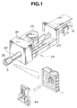
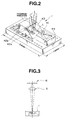
reference numeral 1, is arranged to output a focus error signal E. Referring also to Figs. 1-3, theoptical detector 1 comprises a one-chip optical integrated circuit (IC) 44, alaser diode 41 as a light source, aprism 43 for reflecting laser light L emitted by thelaser diode 41 to anobjective lens 5, and a plurality of light receivingelements 42a, 42b for receiving laser light L reflected by asurface 6 to be measured. Theoptical detector 1 has a small outside dimension of, e.g., 6.5 [mm] x 7.5 [mm] x 1.4 [mm], and includes component parts arranged with accuracy. Theoptical detector 1 can be mass-produced, and at least half reduced in size by a further development of the integration technique. - As shown in Figs. 1 and 4, the one-chip
optical IC 44 of theoptical detector 1, theobjective lens 5, and a member (no numeral) for supporting the two at a predetermined distance constitute anoptical tracer 35. - The
optical tracer 35 is arranged through aspindle 40 to amain body 34 which comprises anactuator 16 having a movingcoil 17 and apermanent magnet 18, alinear scale 20, a detectinghead 25, a connectingmember 27, and mountingreference plane 45. - It is to be noted that a lead wire of the one-chip
optical IC 44 of theoptical detector 1 may be connected to a pre-amplifier 2 directly, or with a support of a support member (not shown), etc. For more compact constitution, the lead wire of the one-chipoptical IC 44 may be disposed in a cavity formed in thespindle 40 in the longitudinal direction thereof. - As best seen in Figs. 2 and 3, laser light L emitted by the
laser diode 41 of the one-chipoptical IC 44 is reflected by theprism 43 toward theobjective lens 5 with a focal length f₁. Laser light L incident on theobjective lens 5 is condensed to thesurface 6 by theobjective lens 5. - Laser light L reflected by the
surface 6 is incident on theobjective lens 5, then on theprism 43. Laser light L incident on theprism 43 is detected by the plurality oflight receiving elements 42a, 42b disposed before and behind a focused position. - By way of example, referring to Fig. 5A, each of the
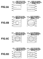
light receiving elements 42a, 42b is in the form of a photodetector array having four strip-shaped photodetectors a₁-a₄, b₁-b₄ disposed in parallel rows. These two sets of photodetector arrays a₁-a₄, b₁-b₄ are disposed to be symmetrical with respect to the focused position. Referring to Figs 5B-5D, a detection of the focused position is carried out by making a comparison between the magnitudes of the diameters of spots of light falling on the two sets of photodetector arrays a₁-a₄, b₁-b₄. When theobjective lens 5 is farther than the focal length f₁ with respect to thesurface 6, the diameter of the spot of light falling on the photodetector array a₁-a₄ disposed before the focused position is smaller than that of the spot of light falling on the photodetector array b₁-b₄ disposed behind the focused position as shown in Fig. 5B. When the distance between theobjective lens 5 and thesurface 6 is equal to the focal length f₁, the two spots of light falling on the photodetector arrays a₁-a₄, b₁-b₄ have the same diameter as shown in Fig. 5C. When theobjective lens 5 is nearer than the focal length f₁ with respect to thesurface 6, the diameter of the spot of light falling on the photodetector array a₁-a₄ before the focused position is larger than that of the spot of light falling on the photodetector array b₁-b₄ behind the focused position as shown in Fig. 5D. - In such a way, the diameters of the spots of light falling on the
light receiving elements 42a, 42b are varied with the distance between theobjective lens 5 and thesurface 6. It is thus understood that the focused position can be detected on an output change of each of the photodetectors a₁-a₄, b₁-b₄. The focus error signal E is generated which is expressed by the following equation:

It is to be noted that each light receiving element may be a four-division diode disclosed in the aforementioned JP-A 4-366711. Referring to Fig. 6, a graph has an x-axis indicative of the distance "d" [mm] between theobjective lens 5 and thesurface 6, and a y-axis indicative of a voltage level V [v] of the focus error signal E. The origin O is indicative of the focused position where the focal length f₁ is equal to the distance "d" between theobjective lens 5 and thesurface 6. - Referring again to Fig. 4, the focus error signal E with a characteristic as illustrated in Fig. 6 is provided to a
servo control circuit 15 which comprises a comparator circuit and a servo amplifier, and provides a drive signal S1 to the movingcoil 17 of theactuator 16 so that the focus error signal E is 0. - The
actuator 16 comprises the movingcoil 17, thepermanent coil 18, and a rod-shaped connectingmember 27. The movingcoil 17 has one end secured to one end of the connectingmember 27, and theoptical tracer 35 is secured to another end of the connectingmember 27 through thespindle 40. - Moreover, the
scale 20 withgraduations 19 is secured to the connectingmember 27 in a predetermined position thereof. Thegraduations 19 of thelinear scale 20 are found on an extension line of theoptical axis 21. In other words, thelinear scale 20 is disposed on an axis which is in line with theoptical axis 21. - It is to be noted that the
linear scale 20 may be an optical scale with interference fringes recorded as thegraduations 19. Moreover, a magnetic scale or a capacitive scale may be used. - The
graduations 19 of thelinear scale 20 can be detected by a detectinghead 25 secured to a chassis or the like with the mountingreference plane 45. It is to be noted that the mountingreference plane 45 may be arranged on only on face of the chassis or the like, or on each of four faces thereof. - Thus, with a displacement of the
linear scale 20, the detectinghead 25 provides an output signal to asignal processing circuit 26, enabling a detection of the displacement amount of thelinear scale 20. The displacement amount of thelinear scale 20 as detected is provided to an indicator or a data logger (not shown) from thesignal processing circuit 26. - In this embodiment, the
linear scale 20 is connected to the connectingmember 27 so as to be movable, whereas the detectinghead 25 is secured to the chassis or the like. Alternatively, thelinear scale 20 may be secured to the chassis or the like, whereas the detectinghead 25 may be connected to the connectingmember 27 so as to be movable. - In that case, as described above, the
servo control circuit 15 provides the drive signal S1 to the movingcoil 17 of theactuator 16 so that the focus error signal E is 0. - Thus, the distance "d" between the
objective lens 5 of theoptical tracer 35 integrally mounted to the movingcoil 17 through the connectingmember 27 andspindle 40 and thesurface 6 is controlled in a feedback way to always have a value equal to the focal length f₁ of theobjective lens 5. This means that the displacement detecting system of the present invention can follow a fine displacement of thesurface 6. - Therefore, when having a displacement of the
surface 6, theoptical tracer 35 is moved to maintain the focal length f₁. This movement of theoptical tracer 35 is indicated on thegraduations 19 of thelinear scale 20, which is read by the detectinghead 25, enabling a detection of a displacement of thesurface 6. In response to an output signal of the detectinghead 25, the displacement amount of thesurface 6 can be calculated in thesignal processing circuit 26. - The displacement amount of the
surface 6 as calculated can be indicated on the indicator (not shown) or recorded in the data logger (not shown), allowing an easy automatic measurement. An execution of interpolation processing in thesignal processing circuit 26 enables a measurement of the displacement amount of thesurface 6 with high resolving power. - Since the
linear scale 20 or the detectinghead 25 which is movable together with theoptical tracer 35 in the direction of theoptical axis 21, etc. is disposed on the axis which is in line with theoptical axis 21 of theobjective lens 5, the displacement amount of thesurface 6 as obtained in such a way has no Abbe error produced due to an inclination of thelinear scale 20 or the detectinghead 25. As a result, the displacement amount of thelinear scale 20 or the detectinghead 25 is in one-to-one correspondence with the displacement amount of theobjective lens 5, resulting in a detection of the displacement amount of thesurface 6 with very high accuracy. - Further, a wide detection range corresponding to a detection range of the
linear scale 20 or a full scale of thegraduations 19 is ensured without any deterioration of detection accuracy. - Furthermore, due to feedback control, even if the sensitivity of the focus error signal E is varied with the reflectance of the
surface 6, there is no occurrence of a measurement error, nor occurrence of an error resulting from a dispersion or drift of elements of theservo control circuit 15 and theactuator 16, resulting in a saving of time for adjustment and calibration of the displacement detecting system, and a long and stable detection of a displacement of thesurface 6. - Referring to Fig. 1, the
actuator 16 is in the form of a voice coil motor, having an excellent linearity with respect to a displacement of thesurface 6. This is due to the fact that the voice coil motor is a motor which presents a linear displacement with respect to current provided to the movingcoil 17. It will be thus understood that a measurement of current provided to the movingcoil 17 allows an easy detection of the displacement amount of thesurface 6. It is to be noted that theactuator 16 is not limited to the voice coil motor, and may be a DC servo motor, a stepping motor, or a voltage element. - Moreover, the method of obtaining the focus error signal E may be the optical astigmatic method, critical angle detecting method, or knife edge method. Any of these methods carries out a control so that the focus error signal E is 0, enabling a detection of a displacement of the
surface 6 with accuracy even if the reflectance thereof is different. - If a
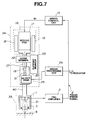
scale origin 31 is formed on thelinear scale 20, the displacement amount of thesurface 6 can be detected with respect to a position of thescale origin 31 as a reference position. - Referring to Fig. 7, another preferred embodiment of the present invention will be described. The another preferred embodiment is substantially the same as the above one preferred embodiment except a
guide member 32 through which the connectingmember 27 is arranged. It is desirable that theguide member 32 is disposed on the extension line of theoptical axis 21 of theobjective lens 5 and at the back of thelinear scale 20 so as to obtain improved running accuracy. Theguide member 32 and the detectinghead 25 are mounted to asupport member 33 which is secured to the chassis (not shown). - In such as way, according to this embodiment, the disposition of the
guide member 32 contributes to an improvement of a running accuracy of the connectingmember 27, resulting in improved read accuracy of the detectinghead 25 with respect to thelinear scale 20. A guide mechanism of theguide member 32 may be of the contact type such as a bearing or the like, or of the non-contact type using a magnet or an air slide which enables a construction of the displacement detecting system with higher accuracy. - Referring to Fig. 8, the other preferred embodiment of the present invention will be described. The other preferred embodiment is substantially the same as the one preferred embodiment except a constitution of the
spindle 40. That is, thespindle 40 is connected to thelinear scale 20 at a lower end thereof. Thespindle 40 has a cavity in the longitudinal direction thereof. The one-chipoptical IC 44 of theoptical detector 1 is arranged in the cavity of thespindle 40 at one end thereof on the side of thelinear scale 20. Moreover, acollimator lens 36 is arranged in the cavity of thespindle 40 at the one end thereof on the side of thelinear scale 20 and below the one-chipoptical IC 44. Theobjective lens 6 is arranged in thecavity 40 at another end thereof. Thespindle 40, which includes theoptical detector 35, is constructed so that a portion having the one-chipoptical IC 44 of theoptical detector 1 and thecollimator 36 is covered by themain body 34. - According to this embodiment, since the one-chip
optical IC 44 of theoptical detector 1 is arranged in the cavity of thespindle 44 and inside of themain body 34, thespindle 40 can have a pointed end as thinned, resulting in a space-saving. - Having described the present invention in connection with the preferred embodiments, it is to be noted that the present invention is not limited thereto, and various changes and modifications can be made without departing from the spirit of the present invention.
Claims (14)
- A system for detecting a displacement of a surface, comprising:
an objective lens movably disposed apart from the surface, said objective lens having a predetermined focal length and an optical axis;
one-chip optical integrated circuit means for producing laser light and generating in response to laser light reflected by the surface a focus error signal indicative of a deviation of a distance between the surface and said objective lens from said predetermined focal length;
control circuit means, connected to said one-chip optical integrated circuit means, for generating a drive signal so that said focus error signal is null;
means for moving in response to said drive signal said objective lens in a direction of said optical axis thereof; and
means for detecting a displacement amount of said objective lens. - A system as claimed in claim 1, further comprising a spindle interposed between a main body having said objective lens moving means and said displacement detecting means and an optical tracer having said objective lens and said one-chip optical integrated circuit means, and a connecting member interposed between said objective lens moving means and said optical tracer.
- A system as claimed in claim 2, wherein said spindle is formed with a cavity in a longitudinal direction thereof, in which a lead wire of said one-chip optical integrated circuit means is disposed.
- A system as claimed in claim 3, wherein said cavity of said spindle has one end portion facing said main body wherein said one-chip optical integrated circuit means and a collimator lens are disposed, and another end portion facing the surface wherein said objective lens is disposed, said one end portion being covered by said main body.
- A system as claimed in claim 1, wherein said one-chip optical integrated circuit means include a laser diode, a plurality of light receiving elements, and a prism.
- A system as claimed in claim 1, wherein said control circuit means include a comparator circuit and a servo amplifier.
- A system as claimed in claim 1, wherein said objective lens moving means include an actuator having a moving coil and a permanent coil.
- A system as claimed in claim 1, wherein said displacement detecting means include a linear scale and a detecting head, one of which being disposed on an axis which is in line with said optical axis of said objective lens.
- A system as claimed in claim 5, wherein said plurality of light receiving elements are in a form of a photodetector array having a plurality of strip-shaped photodetectors disposed in parallel rows.
- A system as claimed in claim 7, wherein said actuator includes a voice coil motor, a DC servo motor, a stepping motor, and a voltage element.
- A system as claimed in claim 8, wherein said linear scale is of an optical type, a magnetic type, and a capacitive type.
- A system as claimed in claim 1, wherein said error signal is obtained by an optical astigmatic method, a critical angle detecting method, and a knife edge method
- A system as claimed in claim 2, further comprising a guide member through which said connecting member is arranged, and a support member for supporting said guide member.
- A system for detecting a displacement of a surface, comprising:
a source of laser light;
an objective lens movably disposed apart from the surface, said objective lens condensing laser light of said source to the surface, said objective lens having a predetermined focal length and an optical axis;
means for generating in response to laser light reflected by the surface a focus error signal indicative of a deviation of a distance between the surface and said objective lens from said predetermined focal length;
control circuit means, connected to said focus error signal generating means, for generating a drive signal so that said focus error signal is null;
means for moving in response to said drive signal said objective lens in a direction of said optical axis thereof; and
means for detecting a displacement amount of said objective lens,
wherein said source of laser light and said focus error signal generating means are in a form of a one-chip optical integrated circuit.
Applications Claiming Priority (2)
| Application Number | Priority Date | Filing Date | Title |
|---|---|---|---|
| JP253175/93 | 1993-10-08 | ||
| JP25317593A JP3413503B2 (en) | 1993-10-08 | 1993-10-08 | Displacement detector |
Publications (3)
| Publication Number | Publication Date |
|---|---|
| EP0647835A2 true EP0647835A2 (en) | 1995-04-12 |
| EP0647835A3 EP0647835A3 (en) | 1996-11-06 |
| EP0647835B1 EP0647835B1 (en) | 1999-04-07 |
Family
ID=17247586
Family Applications (1)
| Application Number | Title | Priority Date | Filing Date |
|---|---|---|---|
| EP94115864A Expired - Lifetime EP0647835B1 (en) | 1993-10-08 | 1994-10-07 | Displacement detecting system |
Country Status (4)
| Country | Link |
|---|---|
| US (1) | US5521394A (en) |
| EP (1) | EP0647835B1 (en) |
| JP (1) | JP3413503B2 (en) |
| DE (1) | DE69417673T2 (en) |
Cited By (1)
| Publication number | Priority date | Publication date | Assignee | Title |
|---|---|---|---|---|
| EP2431826A1 (en) * | 2004-05-27 | 2012-03-21 | K.U.Leuven Research & Development | A measurement configuration based on linear scales able to measure to a target also moving perpendicular to the measurement axis |
Families Citing this family (5)
| Publication number | Priority date | Publication date | Assignee | Title |
|---|---|---|---|---|
| JP2009258022A (en) * | 2008-04-18 | 2009-11-05 | Sony Corp | Displacement detecting device |
| CN103411543B (en) * | 2013-08-07 | 2016-01-20 | 厦门大学 | Screw lead precision testing device and gauge head unit thereof |
| CN103940342B (en) * | 2014-03-28 | 2017-02-22 | 北京工业大学 | Double-rolling type arc-surface cam machining precision detecting device |
| US11577859B1 (en) * | 2019-10-08 | 2023-02-14 | Rockwell Collins, Inc. | Fault resilient airborne network |
| US11921344B2 (en) * | 2020-01-20 | 2024-03-05 | Lecc Technology Co., Ltd. | Laser module |
Citations (5)
| Publication number | Priority date | Publication date | Assignee | Title |
|---|---|---|---|---|
| EP0258450A1 (en) * | 1986-02-24 | 1988-03-09 | Sony Corporation | Device for detecting focus |
| WO1988002846A1 (en) * | 1986-10-20 | 1988-04-21 | Renishaw Plc | Optical measuring probe |
| EP0301792A2 (en) * | 1987-07-31 | 1989-02-01 | Sony Corporation | An optical pickup device |
| DE4219311A1 (en) * | 1991-06-13 | 1992-12-17 | Sony Magnescale Inc | SHIFT DETECTOR |
| EP0646769A1 (en) * | 1993-10-05 | 1995-04-05 | Sony Magnescale, Inc. | Displacement measurement apparatus |
Family Cites Families (3)
| Publication number | Priority date | Publication date | Assignee | Title |
|---|---|---|---|---|
| US5144603A (en) * | 1990-03-07 | 1992-09-01 | Hitachi, Ltd. | Optical head incorporating refractive index distribution changeable lens |
| JPH0460933A (en) * | 1990-06-26 | 1992-02-26 | Matsushita Electric Ind Co Ltd | Optical pickup head device |
| JP3256984B2 (en) * | 1991-06-13 | 2002-02-18 | ソニー・プレシジョン・テクノロジー株式会社 | Displacement detector |
-
1993
- 1993-10-08 JP JP25317593A patent/JP3413503B2/en not_active Expired - Fee Related
-
1994
- 1994-10-06 US US08/319,104 patent/US5521394A/en not_active Expired - Lifetime
- 1994-10-07 DE DE69417673T patent/DE69417673T2/en not_active Expired - Lifetime
- 1994-10-07 EP EP94115864A patent/EP0647835B1/en not_active Expired - Lifetime
Patent Citations (5)
| Publication number | Priority date | Publication date | Assignee | Title |
|---|---|---|---|---|
| EP0258450A1 (en) * | 1986-02-24 | 1988-03-09 | Sony Corporation | Device for detecting focus |
| WO1988002846A1 (en) * | 1986-10-20 | 1988-04-21 | Renishaw Plc | Optical measuring probe |
| EP0301792A2 (en) * | 1987-07-31 | 1989-02-01 | Sony Corporation | An optical pickup device |
| DE4219311A1 (en) * | 1991-06-13 | 1992-12-17 | Sony Magnescale Inc | SHIFT DETECTOR |
| EP0646769A1 (en) * | 1993-10-05 | 1995-04-05 | Sony Magnescale, Inc. | Displacement measurement apparatus |
Cited By (1)
| Publication number | Priority date | Publication date | Assignee | Title |
|---|---|---|---|---|
| EP2431826A1 (en) * | 2004-05-27 | 2012-03-21 | K.U.Leuven Research & Development | A measurement configuration based on linear scales able to measure to a target also moving perpendicular to the measurement axis |
Also Published As
| Publication number | Publication date |
|---|---|
| JP3413503B2 (en) | 2003-06-03 |
| DE69417673D1 (en) | 1999-05-12 |
| EP0647835A3 (en) | 1996-11-06 |
| DE69417673T2 (en) | 1999-07-29 |
| JPH07110212A (en) | 1995-04-25 |
| EP0647835B1 (en) | 1999-04-07 |
| US5521394A (en) | 1996-05-28 |
Similar Documents
| Publication | Publication Date | Title |
|---|---|---|
| US5982494A (en) | Non-contact position sensor | |
| US5172002A (en) | Optical position sensor for scanning probe microscopes | |
| US6430833B1 (en) | Measuring probe with diaphragms and modules | |
| US4897536A (en) | Optical axis displacement sensor with cylindrical lens means | |
| JP3473057B2 (en) | Displacement detector | |
| EP0415579A1 (en) | Touch probe | |
| JP3308230B2 (en) | Maintaining device and method for maintaining target separation distance between object of main optical system and optical output stage | |
| US6459492B1 (en) | Non-contact position sensor | |
| US6181422B1 (en) | Optical surface measurement apparatus and methods | |
| US4987292A (en) | Method and apparatus for detecting focus and tracking errors | |
| EP0234562A2 (en) | Displacement sensor | |
| US5521394A (en) | Compact displacement detecting system with optical integrated circuit and connector in-line with optical axis | |
| KR20000069318A (en) | Device for optically scanning a record carrier | |
| EP0884564B1 (en) | Displacement sensor and method for producing target feature thereof | |
| JP3256984B2 (en) | Displacement detector | |
| US7054095B2 (en) | Displacement detection apparatus, and magnetic recording apparatus and encoder using the displacement detection apparatus | |
| US4766305A (en) | Optical surface test apparatus for testing constricted surface areas | |
| KR100498192B1 (en) | Non-contact position sensor | |
| JP3261332B2 (en) | Optical displacement measuring device | |
| JPH033176B2 (en) | ||
| JPH074914A (en) | Optical minute displacement/roughness gage | |
| JPH07167620A (en) | Laser measuring method and measuring stylus | |
| JPH09210620A (en) | Surface position detection device | |
| Heeren et al. | An Optical System to | |
| JPS58100754A (en) | Acceleration sensor |
Legal Events
| Date | Code | Title | Description |
|---|---|---|---|
| PUAI | Public reference made under article 153(3) epc to a published international application that has entered the european phase |
Free format text: ORIGINAL CODE: 0009012 |
|
| 17P | Request for examination filed |
Effective date: 19941007 |
|
| AK | Designated contracting states |
Kind code of ref document: A2 Designated state(s): CH DE FR GB LI NL |
|
| PUAL | Search report despatched |
Free format text: ORIGINAL CODE: 0009013 |
|
| AK | Designated contracting states |
Kind code of ref document: A3 Designated state(s): CH DE FR GB LI NL |
|
| 17Q | First examination report despatched |
Effective date: 19970520 |
|
| GRAG | Despatch of communication of intention to grant |
Free format text: ORIGINAL CODE: EPIDOS AGRA |
|
| RAP1 | Party data changed (applicant data changed or rights of an application transferred) |
Owner name: SONY PRECISION TECHNOLOGY INC. |
|
| GRAG | Despatch of communication of intention to grant |
Free format text: ORIGINAL CODE: EPIDOS AGRA |
|
| GRAH | Despatch of communication of intention to grant a patent |
Free format text: ORIGINAL CODE: EPIDOS IGRA |
|
| GRAH | Despatch of communication of intention to grant a patent |
Free format text: ORIGINAL CODE: EPIDOS IGRA |
|
| GRAA | (expected) grant |
Free format text: ORIGINAL CODE: 0009210 |
|
| AK | Designated contracting states |
Kind code of ref document: B1 Designated state(s): CH DE FR GB LI NL |
|
| REG | Reference to a national code |
Ref country code: CH Ref legal event code: NV Representative=s name: PATENTANWALTSBUERO JEAN HUNZIKER Ref country code: CH Ref legal event code: EP |
|
| REF | Corresponds to: |
Ref document number: 69417673 Country of ref document: DE Date of ref document: 19990512 |
|
| ET | Fr: translation filed | ||
| PLBE | No opposition filed within time limit |
Free format text: ORIGINAL CODE: 0009261 |
|
| STAA | Information on the status of an ep patent application or granted ep patent |
Free format text: STATUS: NO OPPOSITION FILED WITHIN TIME LIMIT |
|
| 26N | No opposition filed | ||
| REG | Reference to a national code |
Ref country code: GB Ref legal event code: IF02 |
|
| PGFP | Annual fee paid to national office [announced via postgrant information from national office to epo] |
Ref country code: FR Payment date: 20101104 Year of fee payment: 17 |
|
| PGFP | Annual fee paid to national office [announced via postgrant information from national office to epo] |
Ref country code: GB Payment date: 20101021 Year of fee payment: 17 |
|
| REG | Reference to a national code |
Ref country code: CH Ref legal event code: PUE Owner name: MAGNESCALE CO., LTD. Free format text: SONY PRECISION TECHNOLOGY INC.#9-17 NISHIGOTANDA 3-CHOME,#SHINAGAWA-KU TOKYO (JP) -TRANSFER TO- MAGNESCALE CO., LTD.#SHINAGAWA INTERCITY TOWER A-18F 2-15-1 KONAN#MINATU-KU TOKYO 108-6018 (JP) |
|
| REG | Reference to a national code |
Ref country code: NL Ref legal event code: SD Effective date: 20110630 |
|
| REG | Reference to a national code |
Ref country code: GB Ref legal event code: 732E Free format text: REGISTERED BETWEEN 20110728 AND 20110803 |
|
| GBPC | Gb: european patent ceased through non-payment of renewal fee |
Effective date: 20111007 |
|
| REG | Reference to a national code |
Ref country code: FR Ref legal event code: ST Effective date: 20120629 |
|
| PG25 | Lapsed in a contracting state [announced via postgrant information from national office to epo] |
Ref country code: GB Free format text: LAPSE BECAUSE OF NON-PAYMENT OF DUE FEES Effective date: 20111007 Ref country code: FR Free format text: LAPSE BECAUSE OF NON-PAYMENT OF DUE FEES Effective date: 20111102 |
|
| REG | Reference to a national code |
Ref country code: DE Ref legal event code: R082 Ref document number: 69417673 Country of ref document: DE Representative=s name: GRUENECKER, KINKELDEY, STOCKMAIR & SCHWANHAEUS, DE |
|
| REG | Reference to a national code |
Ref country code: CH Ref legal event code: PUE Owner name: MORI SEIKO CO.,LTD., JP Free format text: FORMER OWNER: MAGNESCALE CO., LTD., JP |
|
| REG | Reference to a national code |
Ref country code: NL Ref legal event code: SD Effective date: 20130903 |
|
| REG | Reference to a national code |
Ref country code: DE Ref legal event code: R082 Ref document number: 69417673 Country of ref document: DE Representative=s name: GRUENECKER, KINKELDEY, STOCKMAIR & SCHWANHAEUS, DE Effective date: 20130806 Ref country code: DE Ref legal event code: R081 Ref document number: 69417673 Country of ref document: DE Owner name: MORI SEIKI CO., LTD., YAMATOKORIYAMA-SHI, JP Free format text: FORMER OWNER: MAGNESCALE CO., LTD., TOKYO, JP Effective date: 20130806 Ref country code: DE Ref legal event code: R081 Ref document number: 69417673 Country of ref document: DE Owner name: MORI SEIKI CO., LTD., JP Free format text: FORMER OWNER: MAGNESCALE CO., LTD., TOKYO, JP Effective date: 20130806 |
|
| REG | Reference to a national code |
Ref country code: CH Ref legal event code: PK Free format text: BERICHTIGUNG INHABER |
|
| PGFP | Annual fee paid to national office [announced via postgrant information from national office to epo] |
Ref country code: CH Payment date: 20131021 Year of fee payment: 20 Ref country code: DE Payment date: 20131021 Year of fee payment: 20 |
|
| PGFP | Annual fee paid to national office [announced via postgrant information from national office to epo] |
Ref country code: NL Payment date: 20131022 Year of fee payment: 20 |
|
| REG | Reference to a national code |
Ref country code: DE Ref legal event code: R071 Ref document number: 69417673 Country of ref document: DE |
|
| REG | Reference to a national code |
Ref country code: NL Ref legal event code: V4 Effective date: 20141007 Ref country code: CH Ref legal event code: PL |