EP0642045A1 - Circuit intégré optique hybride avec des axes optiques sur des niveaux différents - Google Patents
Circuit intégré optique hybride avec des axes optiques sur des niveaux différents Download PDFInfo
- Publication number
- EP0642045A1 EP0642045A1 EP94108254A EP94108254A EP0642045A1 EP 0642045 A1 EP0642045 A1 EP 0642045A1 EP 94108254 A EP94108254 A EP 94108254A EP 94108254 A EP94108254 A EP 94108254A EP 0642045 A1 EP0642045 A1 EP 0642045A1
- Authority
- EP
- European Patent Office
- Prior art keywords
- optical
- silicon substrate
- optical waveguide
- output
- layer
- Prior art date
- Legal status (The legal status is an assumption and is not a legal conclusion. Google has not performed a legal analysis and makes no representation as to the accuracy of the status listed.)
- Granted
Links
Images


Classifications
-
- G—PHYSICS
- G02—OPTICS
- G02B—OPTICAL ELEMENTS, SYSTEMS OR APPARATUS
- G02B6/00—Light guides; Structural details of arrangements comprising light guides and other optical elements, e.g. couplings
- G02B6/24—Coupling light guides
- G02B6/42—Coupling light guides with opto-electronic elements
-
- G—PHYSICS
- G02—OPTICS
- G02B—OPTICAL ELEMENTS, SYSTEMS OR APPARATUS
- G02B6/00—Light guides; Structural details of arrangements comprising light guides and other optical elements, e.g. couplings
- G02B6/24—Coupling light guides
- G02B6/42—Coupling light guides with opto-electronic elements
- G02B6/4201—Packages, e.g. shape, construction, internal or external details
- G02B6/4204—Packages, e.g. shape, construction, internal or external details the coupling comprising intermediate optical elements, e.g. lenses, holograms
-
- G—PHYSICS
- G02—OPTICS
- G02B—OPTICAL ELEMENTS, SYSTEMS OR APPARATUS
- G02B6/00—Light guides; Structural details of arrangements comprising light guides and other optical elements, e.g. couplings
- G02B6/24—Coupling light guides
- G02B6/42—Coupling light guides with opto-electronic elements
- G02B6/4201—Packages, e.g. shape, construction, internal or external details
- G02B6/4249—Packages, e.g. shape, construction, internal or external details comprising arrays of active devices and fibres
Definitions
- the present invention relates to an integrated optical device, and more particularly to a hybrid integrated optical device having optical fibers, optical waveguides, and optical semiconductor devices respectively integrated on a single substrate.
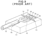
- Fig.9 is a perspective view of a conventional optical IC disclosed in Japanese Patent Laid-open Publication No.57-84189.
- Semiconductor laser guides (recesses) 58 are formed on a substrate 51, and semiconductor lasers 57 are fitted in the semiconductor laser guides 58 and fixed thereto.
- Laser beams emitted from the three semiconductor lasers are converged by a cylindrical lens 54 aligned in a lens guide groove 55 formed on the substrate 51, and guided to three light incident planes of an optical waveguide formed on the substrate 51.
- the optical waveguide 52 guide the three beams incident to the three light incident planes separately at first, and then multiplex or join them at the junction region thereof to output the laser beam from a single output plane thereof.
- a V groove 56 for guiding an optical fiber 53 is formed on the substrate 51, starting from the position corresponding to the light output plane to one end of the substrate 51.
- the optical fiber 53 is fitted in, and fixed to, the V groove 56.
- the positions of the semiconductor lasers 57 and optical fiber 53 are therefore aligned by the semiconductor laser guides 58 and V groove 56 to provide optical coupling therebetween.
- Figs.10A to 10F illustrate two different procedures of forming the optical fiber guiding V groove (hereinafter simply called a V groove) and the optical waveguide of the integrated optical device shown in Fig.9.
- a V groove optical fiber guiding V groove
- Fig.10C an optical waveguide is formed after a V groove has been formed.
- an SiO2 film 62 is formed on the surface of a silicon substrate 61 having the (1 0 0) plane, and an opening 63 to be used for V groove etching is formed in the SiO2 film 62 by photolithography.
- a V groove 64 is formed by anisotropic etching by using potassium hydroxide (KOH) aqueous solution, as shown in Fig.10A.
- a lower cladding layer 65 is formed on the whole surface of the SiO2 film.
- an core region 66 having a relatively high refractive index is formed on the lower cladding layer 65 and patterned.
- An upper cladding layer 67 is then formed on the core region 66.
- the lower cladding layer 65, core region 66, and upper cladding layer 67 are selectively etched to form an end plane of the optical waveguide. This end plane corresponds to light input/output port of the Planar waveguide.
- a lower cladding layer 65, an optical waveguide core layer 66, and upper cladding layer 67 are formed on a silicon substrate 61 in the manner similar to the step of Fig.10D.
- the lower cladding layer 65, core region 66, and upper cladding layer 67 are selectively etched to form an opening 68 to be used for V groove etching.
- the silicon substrate 61 is anisotropically etched to form a V groove 64.
- materials of the optical waveguide components are also deposited on the V groove 64 while the optical waveguide is formed. It is difficult to remove such materials on the V groove while maintaining the designed configurations of the V groove and optical waveguide, because the V groove is as deep as 100 ⁇ m usually.
- the optical waveguide films 65, 66, and 67 are side-etched when the V groove etching opening 68 is formed, because the optical waveguide is thick. It is therefore difficult to form the V groove 64 precisely.
- the semiconductor laser 57 is fitted in the semiconductor laser guide 58 and bonded thereto in a junction-up position (with a heterojunction located upside).
- allowance of the height of the active region of a semiconductor laser is above +/- 10 ⁇ so that it is difficult to make the core region of a waveguide flush with the active layer.
- the width of a semiconductor laser chip and the relative positions of the active region from its opposite side ends have a dimension allowance of above +/- 10 ⁇ . Therefore, the position displacement,less than +/- 3 ⁇ m is usually required for single-mode waveguide, is large if simply a semiconductor laser is fitted in the semiconductor laser guide 58, so that it is difficult to obtain sufficient coupling with an optical waveguide.
- the exposed image of a pattern has blurred edges because of the steps of the optical waveguide and the laser guide groove, so that it is difficult to provide precise position alignment.
- the V groove 56 which is very deep for photolithographic process, prevents fine work.
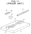
- Fig.11 shows an example of an integrated optical device disclosed in Japanese Patent Laid-open Publication No.61-46911. As shown, an optical fiber guide 72, an optical waveguide 73, and semiconductor laser guides 74 are formed on a substrate 71.
- a semiconductor laser 75 having an active region 75a and a photodetector 76 are aligned with the semiconductor laser guides 74 and fixed thereto.
- the dimension allowance of the height of the active layer of a semiconductor laser and the positions of active region from its opposite side ends is above +/- 10 ⁇ , so that it is difficult to make the active region 75a of the semiconductor laser 75 flush with the core region of the optical waveguide 73.
- the position alignment is particularly difficult if a single mode fiber and a single mode optical waveguide, which usually requires accurate positioning less than +/- 3 ⁇ m, are used.
- Fig.12 shows an example of an integrated optical device disclosed in Japanese Patent Laid-open Publication No.2-58005. As shown, an optical waveguide 87, and bonding pads 81, 82, and 83 are formed on a substrate 80.
- a bonding pad 82 is formed on the bottom of a semiconductor laser 84 and bonded to the bonding pad 82 on the substrate 80.
- the semiconductor laser 84 can be position-aligned precisely because if there is any misalignment, the bonding pad 86 makes a short circuit between the bonding pad 82 and the bonding pad 81 or 83.
- an integrated optical device having: a silicon substrate; a planar optical waveguide which is formed partially on the surface of the silicon substrate, and has a light guiding core region of high refractive index surrounded by a lower-index cladding layer and a flat top surface; a bonding pedestal which is formed partially on the surface of the silicon substrate occupying a portion different from the portion occupying the planar optical waveguide and has a flat top surface, the height of the flat top surface of the bonding pedestal and the planar optical waveguide from the surface of the silicon substrate being the same; V groove having a V-character shaped cross section for position-aligning an optical fiber so as to optically couple the planar optical waveguide and the optical fiber, the V groove being formed on the surface of the silicon substrate along an optical axis extending in one direction from one light input/output port of the optical waveguide; an edge input/output type optical semiconductor device bonded on the top surface of said bonding pedestal, the optical semiconductor device being mounted on a
- the optical axis level changing means includes: a first lens for collimating a light beam emitted from the optical semiconductor device or converging a collimated light beam into the optical semiconductor device; a first lens guide hole formed on the surface of the silicon substrate for position-aligning the first lens on the surface of the silicon substrate; a second lens for converging a collimated light beam into the optical waveguide or collimating a light beam emitted from the optical waveguide; and a second lens guide hole formed on the surface of the silicon substrate for position-aligning the second lens on the surface of the silicon substrate; an optical member for refracting a light beam to change the heights of the optical axes, the optical member being provided between the first and second lenses; and an optical member guide groove formed on the surface of the silicon substrate for position-aligning the optical member on the surface of the silicon substrate.
- the optical member may include a transparent plate made of a material transparent relative to the wavelength of a transmission light beam, the light incident and output planes of the transparent plate being disposed to be inclined by a predetermined angle from an optical axis of incident ray.
- the optical member may include a transparent plate having both opposite planes disposed to be inclined by a predetermined angle from an optical axis, and two support members having one planes disposed perpendicular to an optical axis, and the other planes disposed in tight contact with the light incident and output planes of the transparent plate, the two support members each being formed with a through hole at the region where a light beam transmits.
- a method of forming an integrated optical device including the steps of:forming a V groove and first and second lens guiding grooves for position-aligning lenses by selectively etching the surface of a silicon substrate through anisotropic etching; bonding another silicon substrate having an SiO2 film formed on the surface of the other silicon substrate to the silicon substrate, by directing the SiO2 film to the surface of the silicon substrate; removing the other silicon substrate and leaving the SiO2 film for a planarizing layer; forming a deposited layer for optical waveguide by depositing cladding layer material and core material of core region on the SiO2 film, by patterning the layer for core region through photolithography; and by depositting upper cladding layer material so as to planarize the top surface of the planar waveguide and cover the core region; forming bonding pads for bonding an optical semiconductor device at the place which corresponds to the bonding pedestal on the top surface of the deposited layer for the planar waveguide; selectively etching the deposited
- Bonding pads for bonding an optical semiconductor device can be formed on a flat, top surface of the deposited layers for optical waveguide so that patterns can be formed at high precision. If an optical semiconductor device is flip-chip bonded, the active region of the optical semiconductor device can be positioned at high precision irrespective of its outer dimension.
- An optical axis can be shifted by disposing an optical member to be inclined relative to the optical axis of incident light beam. It is therefore possible to optically couple the optical waveguide and the active region of the optical semiconductor device both having different heights from the substrate surface.
- the optical member may be of a three-layer structure made of transparent optical members having different refractive indices. By inclining the interfaces between the three layers, it is possible to dispose the light incident and output planes perpendicularly to the optical axis. It is therefore possible to improve the position alignment precision of the optical member.
- Birefringence material may be used for the optical member to allow the light incident and output planes to be disposed perpendicularly to the optical axis, to thereby improve the position alignment precision of the optical member.
- the core region of an optical waveguide can be made much higher than the surface of the substrate. Accordingly, the diameter of a laser beam can be made larger to thus improve the optical coupling tolerance.
- an optical semiconductor device such as a semiconductor laser and an optical fiber can be optically coupled with highly precise position alignment without any adjustment. It is therefore possible to easily manufacture a hybrid optical transceiver widely used by optical communications.
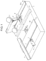
- Fig.1 is a perspective view of an integrated optical device according to a first embodiment of the present invention.
- Figs.2A and 2B are cross sectional views of the integrated optical device of the first embodiment.
- Figs.3A to 3J are cross sectional views explaining a method of manufacturing an integrated optical device according to the first embodiment of the present invention.
- Figs.4A to 4F are cross sectional views explaining a method of manufacturing an integrated optical device according to a second embodiment of the present invention.
- Fig.5 is a perspective view of an integrated optical device according to a third embodiment of the present invention.
- Fig.6 is a perspective view of an integrated optical device according to a fourth embodiment of the present invention.
- Figs.7A and 7B are perspective views of rectangular optical members used by an integrated optical device according to a fifth embodiment of the present invention.
- Fig.8 is a cross sectional view of a rectangular optical member used by an integrated optical device according to a sixth embodiment of the present invention.
- Fig.9 is a perspective view of a conventional integrated optical device.
- Figs.10A to 10F are perspective views explaining conventional methods of forming a V groove and an optical waveguide.
- Fig.11 is a perspective view of a conventional integrated optical device.
- Fig.12 is a perspective view of another conventional integrated optical device.
- Fig.1 is a perspective view of an integrated optical device of the first embodiment
- Figs.2A and 2B are cross sectional views of the device shown in Fig.1.
- Fig.2B is a cross sectional view taken along line IIB-IIB of Fig.2A.
- Optical waveguides 20 are formed partially on the surface of a silicon substrate 1 having the (1 0 0) plane, with an SiO2 film 14 being interposed therebetween.
- the SiO2 film 14 is used for a planarizing layer.
- the optical waveguide 20 is constructed of a lower cladding layer 2, an upper cladding layer 3, and a core region 4 surrounded by the cladding layers 2 and 3.
- the cladding layers are made of SiO2 and the core region is made of a Ge doped SiO2.
- a V groove 5 is formed on the surface of the silicon substrate, extending in one direction along the optical axis from the one end of the waveguide 20 which corresponds to a light input/output port.
- An optical fiber 9 is fitted in, and fixed to, the V groove 5 to provide a position alignment between the optical fiber 9 and the optical waveguide 20.
- a sphere lens 10, a rectangular optical member 12, a sphere lens 11, and an optical semiconductor device 8 are disposed in this order along the optical axis from the other end of the waveguide 20.
- the optical semiconductor device 8 is flip-chip bonded on the layer 20a which corresponds to bonding pedestal.
- the waveguide 20 and the bonding pedestal 20a are formed coincidentally and are formed by the same processes.
- the active region of the optical semiconductor device 8 is therefore at the position higher than the core region 4.
- the sphere lens 10, rectangular optical member 12, and sphere lens 11 are provided.
- V grooves 6 and 7 for guiding the lenses are formed on the surface of the silicon substrate 1.
- the lens guiding V grooves 6 and 7 may be of an up-side-down truncated pyramid shape as shown in Fig.1, or of an up-side-down pyramid shape as shown in Fig.2A.
- the lengths of sides of the pyramid are determined so as to make the optical axis pass through the center of the sphere lenses 10 and 11 which are fitted in the V grooves.
- the rectangular optical member 12 is disposed so that the light incident and output planes of the optical member 12 are tilted by a predetermined angle relative to the optical axis so as to shift the optical axis by a desired height.
- a guide groove 13 is formed on the surface of the silicon substrate 1 for positioning the rectangular optical member 12.
- the width and depth of the guide groove 13 are determined from the thickness of the rectangular optical member 12 so that the optical member 12 inserted into the guide groove 13 can incline by a desired angle.
- the thickness of the silicon substrate is about 1 mm
- the diameter of the optical fiber 9 is 125 ⁇ m
- the diameters of the sphere lenses 10 and 11 are 0.8 mm
- the height of the optical axis of the semiconductor laser 8 from the surface of the bonding pedestal 20a is 6 ⁇ m
- the thickness of the SiO2 film 14 is 2 ⁇ m
- the total thickness of the optical waveguide 20 and bonding pedestal 20a are 28 ⁇ m
- the height of the core 4 of the optical waveguide from the surface of the silicon substrate 1 is 20 ⁇ m.
- Figs.3A to 3J are cross sectional views explaining a method of manufacturing an integrated optical device according to the first embodiment.
- an SiO2 film 12 is formed on the surface of a silicon substrate 1 having the (1 0 0) plane and a thickness of 1 mm. Openings are formed in the SiO2 film 15 at the positions where a V groove 5 and lens guiding grooves 6 and 7 are formed.
- the SiO2 film is selectively etched by potassium hydroxide (KOH) aqueous solution.
- the KOH aqueous solution is anisotropic etchant having a very low etching speed in the (1 1 1) plane so that the (1 1 1) plane appears on the side walls of the etched grooves.
- a thin SiO2 film 15 less than 2 ⁇ m can be used as the etching mask for the V groove 5 and lens guiding V grooves 6 and 7, allowing the V grooves to be etched precisely.
- SiO2 film as thick as above 3 ⁇ m is used as the etching mask, because of KOH aqueous solution slightly corrodes SiO2 and residual SiO2 film must be used as isolator for wiring patterns on the surface.
- a silicon substrate 16 is prepared which is formed with an SiO2 film 14 on the surface of the silicon substrate, the SiO2 film having a thickness of 2 ⁇ m.
- This silicon substrate 16 is bonded to the silicon substrate 1 formed at the process of Fig.3A, by directing the surface with the V grooves of the silicon substrate 1 to the surface with the SiO2 film of the silicon substrate 16.
- This bonding may be performed by using chemical bonding between molecules.
- both the substrates can be bonded together by heating them placed one upon the other at 1000 °C for about one hour.
- a voltage may be applied between the silicon substrates to assist their bonding.
- the silicon substrate 16 is removed by grinding/or polishing and etching.
- the substrate 1 of a two-layer structure can thus be obtained, covering the openings of the V groove 5 and lens guiding V grooves 6 and 7 with the SiO2 film which acts as a planarizing layer.
- a layer for lower cladding layer 2, a core region 4, and upper cladding layer 3 are deposited on the SiO2 film 14.
- the layer for core region 4 is patterned by photoetching to form the core region. Since the V groove 5 and lens guiding V grooves 6 and 7 are covered with the planarizing layer of SiO2 film 14, materials of the optical waveguide components will not enter the V grooves.
- bonding pads 17 for bonding an optical semiconductor device 8 are formed on the layer for cladding layer 3 at predetermined positions.
- a mask 18 is formed covering the bonding pads 17 and the regions where optical waveguide 20 and bonding pedestal 20a are formed.
- an unnecessary region of the deposited layer 20b formed by the layer for cladding layers 2 and 3 and core region and an unnecessary region of the SiO2 film 14 are etched to expose the V groove 5 and lens guiding V grooves 6 and 7.
- An amorphous silicon mask and a reactive-ion-beam-etching technique may be used for the processes respectively.
- the mask 18 is removed to expose the bonding pads 17.
- a rectangular guide groove 13 is formed by using a dicing saw.
- the optical semiconductor device 8 having bonding pads is flip-chip bonded to the bonding pads 17.
- the SiO2 film 14 and optical waveguide 20 are shown thicker than the actual dimension for the easy understanding of the description. In Fig.3H, however, the SiO2 film and optical waveguide 20 are shown thinner matching the actual scale.
- the sphere lenses 10 and 11 and rectangular optical member 12 are fitted in the lens guiding V grooves 6 and 7 and V groove 13, respectively.
- a metal film 19 may be formed on the surface of the cladding layer 3 to enhance heat dissipation.
- a laminated thin optical isolator may be uses as the rectangular optical member 12.
- face-down flip-chip bonding is used for bonding the optical semiconductor device 8 so that position alignment of a relatively high precision can be obtained even if the outer dimension of the optical semiconductor device is different from the original design.
- the integrated optical device manufactured by the embodiment method has a displacement of 2 ⁇ m or less from a target position of the optical semiconductor device.
- the positions and pattern of the bonding pads 17 are precise because they are formed on a flat surface as shown at the process of Fig.3E.
- the second embodiment of the invention will be described with reference to Figs.4A to 4F.
- the second embodiment is characterized by a use of a silicon layer in place of the SiO2 film of the first embodiment, and the other structures are the same as the first embodiment.
- Figs.4A to 4F illustrate the steps of manufacturing an integrated optical device according to the second embodiment of the invention. Similar elements to those shown in Figs.3A to 3J are represented by using identical reference numerals.
- a silicon substrate 1 is prepared which has a V groove 5 and lens guiding V grooves 6 and 7 formed in the manner like the process of Fig.3A.
- This silicon substrate 1 is bonded to another silicon substrate 16, by directing the surface with the V grooves of the silicon substrate 1 to the surface of the silicon substrate 16.
- the silicon substrate 16 is ground and polished to leave the silicon layer having a thickness of 50 ⁇ m. In this manner, a substrate of a two-layer structure is obtained wherein the SiO2 film 14, which serves as an planarizing layer, at the process of Fig.3C of the first embodiment is replaced by the silicon layer 16, which serves as an planarizing layer too.
- a layer for optical waveguide 20b, bonding pads 17, and a mask 18 are formed on the silicon layer 16.
- the layer for optical waveguide 20b is formed by two clad layers and core sandwiched therebetween.
- the layer for optical waveguide 20b is shown as having a single layer.
- the exposed silicon layer 16 is etched out. If a KOH aqueous solution is used as etchant, the surfaces of the V groove 5 and lens guiding V grooves are scarcely etched.
- the silicon layer 16 when the unnecessary region of the layer 20b is etched to leave necessary region for optical waveguides 20 and bonding pedestal 20a, the silicon layer 16 functions as an etching stop layer, thereby improving the etching controllability.
- the height of the optical axis from the surface of the silicon substrate 1 can be made greater.
- the diameter of a light beam can be made large and the optical coupling tolerance can be improved.
- the silicon substrate 16 a single crystal silicon substrate as well as an amorphous silicon substrate can be used. As shown in the side view of Fig.4F and the cross section of Fig.4G, the silicon layer 16 may be left between the SiO2 film 14 and optical waveguide 16 of the first embodiment.
- Fig.5 shows an integrated optical device of the third embodiment.
- the optical waveguide of the integrated optical device shown in Fig.5 has five core regions 4a to 4e and one core region 4 which constitute an optical multiplexer.
- Semiconductor lasers 8a to 8e having different oscillation wavelengths are used as optical semiconductor devices to constitute a light source for multiple wavelength optical communications.
- Laser beams radiated from the semiconductor lasers 8a to 8e pass through sphere lenses 11a to 11e and become incident onto a rectangular optical member 12.
- the optical axes of the laser beams are shifted down by the rectangular optical member 12, and the beams pass through sphere lenses 10a to 10e and become incident onto the core regions 4a to 4c.
- the sphere lenses 10a to 10e, and 11a to 11e are aligned at predetermined positions (in-plane positions and heights) by lens guiding V grooves 6a to 6e, and 7a to 7e., and fixed thereto.
- the rectangular optical member 12 is inclined by a predetermined angle relative to the optical axis by a guide groove 13, and fixed thereto.
- the laser beams incident onto the core regions 4a to 4e are converged to the core regions 4 and become incident onto an optical fiber 9 fixed by the V groove 5.
- an optical multiplexer is formed by a multiplicity of optical semiconductor devices and spherical lenses and optical waveguides.
- a light source for multiple wavelength optical communications can thus be manufactured without any adjustment.
- an integrated optical device having an optical demultiplexer (wave-dividing) function may be formed.
- Fig.6 shows an integrated optical device of the fourth embodiment.
- the optical waveguide is used as a pitch changing means for changing a 1000 ⁇ m pitch suitable for sphere lenses to a 250 ⁇ m pitch suitable for optical fibers.
- This integrated optical device forms a 5-channel parallel light source having five semiconductor lasers optically coupled to ribbon fibers having a pitch of 250 ⁇ m via an optical waveguide having a pitch convertor.
- the structures of semiconductor lasers 8a to 8e and core regions 4a to 4e are the same as those of the third embodiment shown in Fig.3 except for each core regions being separated.
- the semiconductor lasers 8a to 8e, sphere lenses 11a to 11e, and 10a to 10e, and the core regions 4a to 4e on the sphere lens side, are all disposed at the pitch of 1000 ⁇ m.
- the pitch of the core regions 4a to 4e are made narrower toward the optical fiber side, and is set to 250 ⁇ m on the side of the ends of the optical fibers.
- Laser beams radiated from the semiconductor lasers 8a to 8e are made to have a narrowed pitch of 250 ⁇ m, and are incident onto ribbon fibers 9a to 9e aligned at a pitch of 250 ⁇ m by V grooves 5a to 5e.
- a parallel light source can be formed without any adjustment by providing a plurality of optical semiconductor devices, sphere lenses, and optical fibers.
- the pitch change by the optical waveguide reduces inter-channel crosstalk at the electric circuit stage, compared to the case of coupling optical fibers and optical semiconductor devices at a pitch of 250 ⁇ m.
- a semiconductor laser has been used as the optical semiconductor device. If a semiconductor laser is replaced by a photodiode, a light reception device can be realized.
- Fig.7A shows a rectangular optical member 12 of the fifth embodiment.
- the rectangular optical member shown in Fig.7A has a structure that a high refractive index rectangular glass plate 12b are sandwiched between two low refractive index glass plates 12a and 12c.
- a laser beam incident onto the incident plane of, for example, the low refractive index plate 12a refracts at the interface between the low refractive index glass plate 12a and the high refractive index glass plate 12b and at the interface between the high refractive index glass plate 12b and the low refractive index glass plate 12c, resulting in a optical axis shift.
- the same effect as the rectangular optical members 12 of the first to fourth embodiments can therefore be obtained.
- the rectangular optical member 12 of this embodiment can be fitted in the guide groove 13 without any gap, thereby improving a mount precision thereof.
- laser beam pass holes 21 may be formed in glass plates 12d and 12f at the positions where a laser beam passes.
- glass plates 12d, 12e, and 12f having the same refractive index.
- articles made of opaque material may be used instead of the glass plates 12d and 12f.
- Fig.8 shows a cross section of a rectangular optical member 12g cut along the plane of an optical axis 26 of the optical system.
- the rectangular plate optical member 12g uses rutile crystal which is a material having birefringence.
- this rectangular optical member can be fitted in a guide groove without any gap, so that a mount precision can be improved.
- rutile crystal has been used as a material having birefringence.
- Other birefringence materials such as calcite may also be used.
- various types of known materials may be used for an optical waveguide.
- such materials include organic polymer, dielectric material, amorphous semiconductor, films such as an oxidized silicon film and a film of silicon-nitride formed on semiconductor.
- the bonded substrate shown, for example, in Fig.3C is resistant against a high temperature of about 1400 °C so that it can be used for forming a GeO2 - SiO2 based optical waveguide which is formed under a high temperature.
Applications Claiming Priority (3)
| Application Number | Priority Date | Filing Date | Title |
|---|---|---|---|
| JP21663293A JP3302458B2 (ja) | 1993-08-31 | 1993-08-31 | 集積化光装置及び製造方法 |
| JP21663293 | 1993-08-31 | ||
| JP216632/93 | 1993-08-31 |
Publications (2)
| Publication Number | Publication Date |
|---|---|
| EP0642045A1 true EP0642045A1 (fr) | 1995-03-08 |
| EP0642045B1 EP0642045B1 (fr) | 1999-09-15 |
Family
ID=16691482
Family Applications (1)
| Application Number | Title | Priority Date | Filing Date |
|---|---|---|---|
| EP94108254A Expired - Lifetime EP0642045B1 (fr) | 1993-08-31 | 1994-05-27 | Circuit intégré optique hybride avec des axes optiques sur des niveaux différents |
Country Status (4)
| Country | Link |
|---|---|
| US (1) | US5481629A (fr) |
| EP (1) | EP0642045B1 (fr) |
| JP (1) | JP3302458B2 (fr) |
| DE (1) | DE69420652T2 (fr) |
Cited By (8)
| Publication number | Priority date | Publication date | Assignee | Title |
|---|---|---|---|---|
| GB2288035B (en) * | 1994-03-28 | 1997-11-26 | Bosch Gmbh Robert | Integrated optical circuit having detector and optical fibre |
| US5854867A (en) * | 1996-10-29 | 1998-12-29 | Electronics And Telecommunications Research Institute | Optical module having lenses aligned on lens-positioning V-groove and fabrication method thereof |
| WO2002079843A1 (fr) * | 2001-03-28 | 2002-10-10 | Iljin Corporation | Module optique de type enfichable |
| WO2002079812A2 (fr) * | 2001-03-28 | 2002-10-10 | Iljin Corporation | Module optique de taille reduite |
| WO2002079845A1 (fr) * | 2001-03-28 | 2002-10-10 | Iljin Corporation | Module optique petit équipé d'un guide d'ondes optique |
| WO2002079844A1 (fr) * | 2001-03-28 | 2002-10-10 | Iljin Corporation | Module optique a petites formes |
| GB2395066A (en) * | 2002-11-01 | 2004-05-12 | Optitune Plc | Flip chip bonding and passive alignment of optical devices |
| EP3994777A4 (fr) * | 2019-07-02 | 2023-02-01 | Aayuna Inc. | Moteur laser supportant de multiples sources laser |
Families Citing this family (82)
| Publication number | Priority date | Publication date | Assignee | Title |
|---|---|---|---|---|
| JPH07240534A (ja) * | 1993-03-16 | 1995-09-12 | Seiko Instr Inc | 光電変換半導体装置及びその製造方法 |
| US5559915A (en) * | 1995-04-13 | 1996-09-24 | Lucent Technologies Inc. | Apparatuses and methods for aligning an optical fiber array with an optical integrated circuit assembly |
| EP1018050B1 (fr) * | 1995-06-30 | 2001-12-12 | The Whitaker Corporation | Dispositif d'alignement pour un composant optoelectronique |
| US5960259A (en) * | 1995-11-16 | 1999-09-28 | Matsushita Electric Industrial Co., Ltd. | Optical apparatus and method for producing the same |
| US5835650A (en) * | 1995-11-16 | 1998-11-10 | Matsushita Electric Industrial Co., Ltd. | Optical apparatus and method for producing the same |
| JP2964941B2 (ja) * | 1996-01-12 | 1999-10-18 | 日本電気株式会社 | 光デバイスの製造方法及び実装構造 |
| US5793913A (en) * | 1996-07-10 | 1998-08-11 | Northern Telecom Limited | Method for the hybrid integration of discrete elements on a semiconductor substrate |
| US5771323A (en) * | 1996-08-28 | 1998-06-23 | Hewlett-Packard Company | Micro-photonics module |
| US5734771A (en) * | 1996-10-28 | 1998-03-31 | Lucent Technologies Inc. | Packaging assembly for a laser array module |
| US5706371A (en) * | 1996-12-03 | 1998-01-06 | E-Tek Dynamics, Inc. | Optical isolator array device |
| US6023540A (en) | 1997-03-14 | 2000-02-08 | Trustees Of Tufts College | Fiber optic sensor with encoded microspheres |
| US6327410B1 (en) | 1997-03-14 | 2001-12-04 | The Trustees Of Tufts College | Target analyte sensors utilizing Microspheres |
| US7622294B2 (en) * | 1997-03-14 | 2009-11-24 | Trustees Of Tufts College | Methods for detecting target analytes and enzymatic reactions |
| US20030027126A1 (en) * | 1997-03-14 | 2003-02-06 | Walt David R. | Methods for detecting target analytes and enzymatic reactions |
| US6406845B1 (en) | 1997-05-05 | 2002-06-18 | Trustees Of Tuft College | Fiber optic biosensor for selectively detecting oligonucleotide species in a mixed fluid sample |
| US5930429A (en) * | 1997-07-01 | 1999-07-27 | Hewlett-Packard Company | Micro-photonics module integrated on a single substrate |
| US5937114A (en) * | 1997-07-21 | 1999-08-10 | Hewlett-Packard Company | Micro-photonics module with a partition wall |
| US6327289B1 (en) * | 1997-09-02 | 2001-12-04 | Matsushita Electric Industrial Co., Ltd. | Wavelength-variable semiconductor laser, optical integrated device utilizing the same, and production method thereof |
| US7348181B2 (en) | 1997-10-06 | 2008-03-25 | Trustees Of Tufts College | Self-encoding sensor with microspheres |
| US7115884B1 (en) | 1997-10-06 | 2006-10-03 | Trustees Of Tufts College | Self-encoding fiber optic sensor |
| US5987196A (en) * | 1997-11-06 | 1999-11-16 | Micron Technology, Inc. | Semiconductor structure having an optical signal path in a substrate and method for forming the same |
| US5981975A (en) * | 1998-02-27 | 1999-11-09 | The Whitaker Corporation | On-chip alignment fiducials for surface emitting devices |
| US6085007A (en) * | 1998-02-27 | 2000-07-04 | Jiang; Ching-Long | Passive alignment member for vertical surface emitting/detecting device |
| US6210910B1 (en) | 1998-03-02 | 2001-04-03 | Trustees Of Tufts College | Optical fiber biosensor array comprising cell populations confined to microcavities |
| US6188477B1 (en) | 1998-05-04 | 2001-02-13 | Cornell Research Foundation, Inc. | Optical polarization sensing apparatus and method |
| US7060431B2 (en) | 1998-06-24 | 2006-06-13 | Illumina, Inc. | Method of making and decoding of array sensors with microspheres |
| US7510841B2 (en) * | 1998-12-28 | 2009-03-31 | Illumina, Inc. | Methods of making and using composite arrays for the detection of a plurality of target analytes |
| US6429027B1 (en) | 1998-12-28 | 2002-08-06 | Illumina, Inc. | Composite arrays utilizing microspheres |
| US6355431B1 (en) | 1999-04-20 | 2002-03-12 | Illumina, Inc. | Detection of nucleic acid amplification reactions using bead arrays |
| US20060275782A1 (en) * | 1999-04-20 | 2006-12-07 | Illumina, Inc. | Detection of nucleic acid reactions on bead arrays |
| US20030215821A1 (en) * | 1999-04-20 | 2003-11-20 | Kevin Gunderson | Detection of nucleic acid reactions on bead arrays |
| US6304695B1 (en) * | 1999-05-17 | 2001-10-16 | Chiaro Networks Ltd. | Modulated light source |
| US6620584B1 (en) | 1999-05-20 | 2003-09-16 | Illumina | Combinatorial decoding of random nucleic acid arrays |
| US6544732B1 (en) * | 1999-05-20 | 2003-04-08 | Illumina, Inc. | Encoding and decoding of array sensors utilizing nanocrystals |
| US8080380B2 (en) * | 1999-05-21 | 2011-12-20 | Illumina, Inc. | Use of microfluidic systems in the detection of target analytes using microsphere arrays |
| US8481268B2 (en) | 1999-05-21 | 2013-07-09 | Illumina, Inc. | Use of microfluidic systems in the detection of target analytes using microsphere arrays |
| DK1218545T3 (da) * | 1999-08-18 | 2012-02-20 | Illumina Inc | Fremgangsmåder til fremstilling af oligonukleotidopløsninger |
| EP1212599A2 (fr) | 1999-08-30 | 2002-06-12 | Illumina, Inc. | Procedes permettant d'ameliorer la detection de signaux dans un jeu d'echantillons |
| US7167615B1 (en) | 1999-11-05 | 2007-01-23 | Board Of Regents, The University Of Texas System | Resonant waveguide-grating filters and sensors and methods for making and using same |
| US7582420B2 (en) | 2001-07-12 | 2009-09-01 | Illumina, Inc. | Multiplex nucleic acid reactions |
| US8076063B2 (en) * | 2000-02-07 | 2011-12-13 | Illumina, Inc. | Multiplexed methylation detection methods |
| US6913884B2 (en) * | 2001-08-16 | 2005-07-05 | Illumina, Inc. | Compositions and methods for repetitive use of genomic DNA |
| US7955794B2 (en) * | 2000-09-21 | 2011-06-07 | Illumina, Inc. | Multiplex nucleic acid reactions |
| DE60136166D1 (de) * | 2000-02-07 | 2008-11-27 | Illumina Inc | Nukleinsäure-nachweisverfahren mit universellem priming |
| US20050214825A1 (en) * | 2000-02-07 | 2005-09-29 | John Stuelpnagel | Multiplex sample analysis on universal arrays |
| ATE360095T1 (de) | 2000-02-07 | 2007-05-15 | Illumina Inc | Nukleinsäure nachweisverfahren mit universellem priming |
| US7611869B2 (en) * | 2000-02-07 | 2009-11-03 | Illumina, Inc. | Multiplexed methylation detection methods |
| US7361488B2 (en) * | 2000-02-07 | 2008-04-22 | Illumina, Inc. | Nucleic acid detection methods using universal priming |
| WO2001059432A2 (fr) * | 2000-02-10 | 2001-08-16 | Illumina, Inc. | Substrats et formats possibles destines a un ensemble de matrices a base de microspheres |
| US6770441B2 (en) | 2000-02-10 | 2004-08-03 | Illumina, Inc. | Array compositions and methods of making same |
| WO2001061043A2 (fr) * | 2000-02-16 | 2001-08-23 | Illumina, Inc. | Genotypage parallele de plusieurs echantillons preleves sur des patients |
| US20050158702A1 (en) * | 2000-09-05 | 2005-07-21 | Stuelpnagel John R. | Cellular arrays comprising encoded cells |
| JP4182631B2 (ja) * | 2000-09-11 | 2008-11-19 | 沖電気工業株式会社 | 光学装置 |
| US20040018491A1 (en) * | 2000-10-26 | 2004-01-29 | Kevin Gunderson | Detection of nucleic acid reactions on bead arrays |
| US6898029B2 (en) * | 2000-11-16 | 2005-05-24 | Shipley Company, L.L.C. | Optical bench with alignment subassembly |
| US20020110328A1 (en) * | 2001-02-14 | 2002-08-15 | Bischel William K. | Multi-channel laser pump source for optical amplifiers |
| US6804770B2 (en) | 2001-03-22 | 2004-10-12 | International Business Machines Corporation | Method and apparatus for using past history to avoid flush conditions in a microprocessor |
| US6621955B2 (en) * | 2001-06-12 | 2003-09-16 | Industrial Technology Research Institute | Method for fabricating integrated micro spherical lens for optical fiber switch and the device made therefrom |
| WO2003069333A1 (fr) | 2002-02-14 | 2003-08-21 | Illumina, Inc. | Traitement des donnees automatique dans des matrices organisees de façon aleatoire |
| US7595883B1 (en) | 2002-09-16 | 2009-09-29 | The Board Of Trustees Of The Leland Stanford Junior University | Biological analysis arrangement and approach therefor |
| US20040259105A1 (en) * | 2002-10-03 | 2004-12-23 | Jian-Bing Fan | Multiplex nucleic acid analysis using archived or fixed samples |
| US7887752B2 (en) * | 2003-01-21 | 2011-02-15 | Illumina, Inc. | Chemical reaction monitor |
| US6943768B2 (en) | 2003-02-21 | 2005-09-13 | Xtellus Inc. | Thermal control system for liquid crystal cell |
| JP2004272143A (ja) * | 2003-03-12 | 2004-09-30 | Oyokoden Lab Co Ltd | 光導波路の光結合装置及びその製造方法 |
| GB2400183A (en) * | 2003-04-01 | 2004-10-06 | Agilent Technologies Inc | Mounting optic fibre and optical waveguide on substrate |
| US7229763B2 (en) * | 2003-04-07 | 2007-06-12 | Beckman Coulter, Inc. | Assay system using labeled oligonucleotides |
| KR20050058794A (ko) * | 2003-12-12 | 2005-06-17 | 엘지전자 주식회사 | 고분자 렌즈와 광섬유를 이용한 광통신용 시준 렌즈계 |
| US20060246576A1 (en) | 2005-04-06 | 2006-11-02 | Affymetrix, Inc. | Fluidic system and method for processing biological microarrays in personal instrumentation |
| US20060276008A1 (en) * | 2005-06-02 | 2006-12-07 | Vesa-Pekka Lempinen | Thinning |
| JP5131856B2 (ja) * | 2006-01-11 | 2013-01-30 | ライトワイヤー,エルエルシー | 薄型soicmos光電集積回路内への広帯域光学結合 |
| JP2007212551A (ja) * | 2006-02-07 | 2007-08-23 | Yokogawa Electric Corp | 光軸調整機構 |
| US20080003667A1 (en) * | 2006-05-19 | 2008-01-03 | Affymetrix, Inc. | Consumable elements for use with fluid processing and detection systems |
| DE102007012224A1 (de) * | 2007-03-12 | 2008-09-25 | Schleifring Und Apparatebau Gmbh | Mehrkanalige reflexionsarme optische Drehkupplung |
| JP4280290B2 (ja) * | 2007-03-28 | 2009-06-17 | Okiセミコンダクタ株式会社 | 光モジュール及びその製造方法 |
| DE102009026632A1 (de) * | 2008-06-06 | 2009-12-10 | Schleifring Und Apparatebau Gmbh | Linsenanordnung mit Lagejustierung |
| US8103140B2 (en) * | 2009-06-01 | 2012-01-24 | Honeywell International Inc. | Interferometric fiber optic gyroscope with silicon optical bench front-end |
| US9523701B2 (en) | 2009-07-29 | 2016-12-20 | Dynex Technologies, Inc. | Sample plate systems and methods |
| GB0913258D0 (en) | 2009-07-29 | 2009-09-02 | Dynex Technologies Inc | Reagent dispenser |
| US20150124225A1 (en) * | 2013-11-07 | 2015-05-07 | Seiko Epson Corporation | Light source device and projector |
| US9933570B2 (en) * | 2016-03-01 | 2018-04-03 | Futurewei Technologies, Inc. | Integration of V-grooves on silicon-on-insulator (SOI) platform for direct fiber coupling |
| WO2019095133A1 (fr) * | 2017-11-15 | 2019-05-23 | Source Photonics (Chengdu) Company Limited | Module de réseau de guides d'ondes et sous-ensemble optique récepteur |
| US20210356683A1 (en) * | 2020-05-13 | 2021-11-18 | Hisense Broadband Multimedia Technologies Co., Ltd. | Optical module |
Citations (4)
| Publication number | Priority date | Publication date | Assignee | Title |
|---|---|---|---|---|
| DE3731311A1 (de) * | 1987-09-17 | 1989-03-30 | Siemens Ag | Kombinierter sende- und empfangsbaustein eines bidirektionalen optischen uebertragungssystems |
| EP0331338A2 (fr) * | 1988-03-03 | 1989-09-06 | AT&T Corp. | Sous-éléments pour circuits intégrés hybrides opto-électroniques |
| DE4013630A1 (de) * | 1989-05-31 | 1990-12-06 | Siemens Ag | Optoelektronischer wandlermodul und verfahren zu dessen herstellung |
| WO1992000538A1 (fr) * | 1990-07-02 | 1992-01-09 | British Telecommunications Public Limited Company | Systeme optique |
Family Cites Families (6)
| Publication number | Priority date | Publication date | Assignee | Title |
|---|---|---|---|---|
| US4466696A (en) * | 1982-03-29 | 1984-08-21 | Honeywell Inc. | Self-aligned coupling of optical fiber to semiconductor laser or LED |
| EP0219356B1 (fr) * | 1985-10-16 | 1989-12-06 | BRITISH TELECOMMUNICATIONS public limited company | Support d'élément mobile |
| US4875750A (en) * | 1987-02-25 | 1989-10-24 | Siemens Aktiengesellschaft | Optoelectronic coupling element and method for its manufacture |
| US4787696A (en) * | 1987-12-18 | 1988-11-29 | Gte Laboratories Incorporated | Mounting apparatus for optical fibers and lasers |
| US5163108A (en) * | 1990-07-11 | 1992-11-10 | Gte Laboratories Incorporated | Method and device for passive alignment of diode lasers and optical fibers |
| FR2694841B1 (fr) * | 1992-08-14 | 1994-09-09 | Commissariat Energie Atomique | Procédé d'hybridation et de positionnement d'un composant opto-électronique et application de ce procédé au positionnement de ce composant par rapport à un guide optique intégré. |
-
1993
- 1993-08-31 JP JP21663293A patent/JP3302458B2/ja not_active Expired - Fee Related
-
1994
- 1994-05-27 EP EP94108254A patent/EP0642045B1/fr not_active Expired - Lifetime
- 1994-05-27 DE DE69420652T patent/DE69420652T2/de not_active Expired - Fee Related
- 1994-05-31 US US08/251,284 patent/US5481629A/en not_active Expired - Lifetime
Patent Citations (4)
| Publication number | Priority date | Publication date | Assignee | Title |
|---|---|---|---|---|
| DE3731311A1 (de) * | 1987-09-17 | 1989-03-30 | Siemens Ag | Kombinierter sende- und empfangsbaustein eines bidirektionalen optischen uebertragungssystems |
| EP0331338A2 (fr) * | 1988-03-03 | 1989-09-06 | AT&T Corp. | Sous-éléments pour circuits intégrés hybrides opto-électroniques |
| DE4013630A1 (de) * | 1989-05-31 | 1990-12-06 | Siemens Ag | Optoelektronischer wandlermodul und verfahren zu dessen herstellung |
| WO1992000538A1 (fr) * | 1990-07-02 | 1992-01-09 | British Telecommunications Public Limited Company | Systeme optique |
Non-Patent Citations (1)
| Title |
|---|
| LEOS '90, Boston, Massachusetts, 4-9 november 1990, Proceedings vol. 2, IEEE, New York, G.E. Blonder: 'Silicon Optical Bench Research at AT&T * |
Cited By (10)
| Publication number | Priority date | Publication date | Assignee | Title |
|---|---|---|---|---|
| GB2288035B (en) * | 1994-03-28 | 1997-11-26 | Bosch Gmbh Robert | Integrated optical circuit having detector and optical fibre |
| US5854867A (en) * | 1996-10-29 | 1998-12-29 | Electronics And Telecommunications Research Institute | Optical module having lenses aligned on lens-positioning V-groove and fabrication method thereof |
| WO2002079843A1 (fr) * | 2001-03-28 | 2002-10-10 | Iljin Corporation | Module optique de type enfichable |
| WO2002079812A2 (fr) * | 2001-03-28 | 2002-10-10 | Iljin Corporation | Module optique de taille reduite |
| WO2002079845A1 (fr) * | 2001-03-28 | 2002-10-10 | Iljin Corporation | Module optique petit équipé d'un guide d'ondes optique |
| WO2002079844A1 (fr) * | 2001-03-28 | 2002-10-10 | Iljin Corporation | Module optique a petites formes |
| WO2002079812A3 (fr) * | 2001-03-28 | 2007-11-01 | Iljin Corp | Module optique de taille reduite |
| GB2395066A (en) * | 2002-11-01 | 2004-05-12 | Optitune Plc | Flip chip bonding and passive alignment of optical devices |
| US7663210B2 (en) | 2002-11-01 | 2010-02-16 | Optitune Plc | Optical component assembly |
| EP3994777A4 (fr) * | 2019-07-02 | 2023-02-01 | Aayuna Inc. | Moteur laser supportant de multiples sources laser |
Also Published As
| Publication number | Publication date |
|---|---|
| DE69420652T2 (de) | 1999-12-30 |
| JPH0774342A (ja) | 1995-03-17 |
| DE69420652D1 (de) | 1999-10-21 |
| EP0642045B1 (fr) | 1999-09-15 |
| US5481629A (en) | 1996-01-02 |
| JP3302458B2 (ja) | 2002-07-15 |
Similar Documents
| Publication | Publication Date | Title |
|---|---|---|
| EP0642045B1 (fr) | Circuit intégré optique hybride avec des axes optiques sur des niveaux différents | |
| KR100802199B1 (ko) | 광모듈 및 그 제조방법 | |
| US6316281B1 (en) | Method for fabricating a hybrid optical integrated circuit employing SOI optical waveguide | |
| EP1561139B1 (fr) | Composant optique pour la propagation en espace libre entre guides d'ondes | |
| US6527455B2 (en) | Multilayer optical fiber coupler | |
| US4735677A (en) | Method for fabricating hybrid optical integrated circuit | |
| US7352066B2 (en) | Silicon based optical vias | |
| US6118917A (en) | Optical fiber passive alignment apparatus using alignment platform | |
| US5644667A (en) | Integrated semiconductor optical devices and method of manufacture employing substrate having alignment groove | |
| KR100198460B1 (ko) | 브이홈에 정렬된 렌즈를 가진 광모듈 및 그 제작방법 | |
| US8755644B2 (en) | Silicon based optical vias | |
| US7218806B2 (en) | Multi-wavelength optical transceiver module, and multiplexer/demultiplexer using thin film filter | |
| JPH09311253A (ja) | 光結合構造とその製造方法 | |
| US7394955B2 (en) | Optical component and method of manufacturing the same | |
| US6361222B1 (en) | Optical device and optical module provided with optical device | |
| US6847491B1 (en) | Hybrid microlens array | |
| KR100865127B1 (ko) | 광모듈 및 그 제조방법 | |
| JP2002357731A (ja) | 光導波路デバイス用チップ及びその製造方法並びに光導波路デバイス | |
| KR20050071967A (ko) | 양방향 광통신 모듈의 광수신기 및 그 제조방법 | |
| JP2000009953A (ja) | 波長分波器とこの波長分波器を備えた光送受信モジュール | |
| KR20000065884A (ko) | 광송수신 모듈 및 그 제조방법 | |
| KR100819309B1 (ko) | 파장분할다중전송 필터 장치 | |
| KR20080056700A (ko) | 광모듈 및 그 제조방법 | |
| JPH10282361A (ja) | 光ファイバ保持部材、導波路型光部品及び光導波路デバイス | |
| KR20090053440A (ko) | 광모듈 및 그 제조방법 |
Legal Events
| Date | Code | Title | Description |
|---|---|---|---|
| PUAI | Public reference made under article 153(3) epc to a published international application that has entered the european phase |
Free format text: ORIGINAL CODE: 0009012 |
|
| AK | Designated contracting states |
Kind code of ref document: A1 Designated state(s): DE |
|
| 17P | Request for examination filed |
Effective date: 19950905 |
|
| 17Q | First examination report despatched |
Effective date: 19980625 |
|
| GRAG | Despatch of communication of intention to grant |
Free format text: ORIGINAL CODE: EPIDOS AGRA |
|
| GRAG | Despatch of communication of intention to grant |
Free format text: ORIGINAL CODE: EPIDOS AGRA |
|
| GRAH | Despatch of communication of intention to grant a patent |
Free format text: ORIGINAL CODE: EPIDOS IGRA |
|
| GRAH | Despatch of communication of intention to grant a patent |
Free format text: ORIGINAL CODE: EPIDOS IGRA |
|
| GRAA | (expected) grant |
Free format text: ORIGINAL CODE: 0009210 |
|
| AK | Designated contracting states |
Kind code of ref document: B1 Designated state(s): DE |
|
| REF | Corresponds to: |
Ref document number: 69420652 Country of ref document: DE Date of ref document: 19991021 |
|
| PLBE | No opposition filed within time limit |
Free format text: ORIGINAL CODE: 0009261 |
|
| STAA | Information on the status of an ep patent application or granted ep patent |
Free format text: STATUS: NO OPPOSITION FILED WITHIN TIME LIMIT |
|
| 26N | No opposition filed | ||
| PGFP | Annual fee paid to national office [announced via postgrant information from national office to epo] |
Ref country code: DE Payment date: 20040603 Year of fee payment: 11 |
|
| PG25 | Lapsed in a contracting state [announced via postgrant information from national office to epo] |
Ref country code: DE Free format text: LAPSE BECAUSE OF NON-PAYMENT OF DUE FEES Effective date: 20051201 |