EP0642028B1 - Mess- und Experimentiersystem zur Erfassung und Bewertung des EMV-Verhaltens elektrischer Geräte, Baugruppen und Schaltungen - Google Patents
Mess- und Experimentiersystem zur Erfassung und Bewertung des EMV-Verhaltens elektrischer Geräte, Baugruppen und Schaltungen Download PDFInfo
- Publication number
- EP0642028B1 EP0642028B1 EP94113567A EP94113567A EP0642028B1 EP 0642028 B1 EP0642028 B1 EP 0642028B1 EP 94113567 A EP94113567 A EP 94113567A EP 94113567 A EP94113567 A EP 94113567A EP 0642028 B1 EP0642028 B1 EP 0642028B1
- Authority
- EP
- European Patent Office
- Prior art keywords
- measuring
- experimenting
- circuit
- interference
- sensor
- Prior art date
- Legal status (The legal status is an assumption and is not a legal conclusion. Google has not performed a legal analysis and makes no representation as to the accuracy of the status listed.)
- Expired - Lifetime
Links
- 238000013461 design Methods 0.000 claims abstract description 10
- 230000006698 induction Effects 0.000 claims description 32
- 239000003990 capacitor Substances 0.000 claims description 30
- 238000000034 method Methods 0.000 claims description 24
- 230000003287 optical effect Effects 0.000 claims description 24
- 239000000523 sample Substances 0.000 claims description 18
- 230000008569 process Effects 0.000 claims description 16
- 230000008878 coupling Effects 0.000 claims description 14
- 238000010168 coupling process Methods 0.000 claims description 14
- 238000005859 coupling reaction Methods 0.000 claims description 14
- 238000000429 assembly Methods 0.000 claims description 11
- 230000000712 assembly Effects 0.000 claims description 11
- 230000001939 inductive effect Effects 0.000 claims description 9
- 238000011835 investigation Methods 0.000 claims description 9
- 238000006243 chemical reaction Methods 0.000 claims description 7
- 238000003780 insertion Methods 0.000 claims description 6
- 230000037431 insertion Effects 0.000 claims description 6
- 238000011156 evaluation Methods 0.000 claims description 5
- 230000001965 increasing effect Effects 0.000 claims description 5
- 230000003068 static effect Effects 0.000 claims description 5
- 238000012545 processing Methods 0.000 claims description 3
- 230000005684 electric field Effects 0.000 claims description 2
- 238000004458 analytical method Methods 0.000 claims 3
- 230000007246 mechanism Effects 0.000 claims 1
- 230000005693 optoelectronics Effects 0.000 claims 1
- 239000010453 quartz Substances 0.000 claims 1
- 230000009467 reduction Effects 0.000 claims 1
- VYPSYNLAJGMNEJ-UHFFFAOYSA-N silicon dioxide Inorganic materials O=[Si]=O VYPSYNLAJGMNEJ-UHFFFAOYSA-N 0.000 claims 1
- 238000004088 simulation Methods 0.000 claims 1
- 238000005259 measurement Methods 0.000 abstract description 19
- 238000002474 experimental method Methods 0.000 abstract description 10
- 230000009471 action Effects 0.000 abstract description 5
- 238000010276 construction Methods 0.000 abstract description 4
- 238000012549 training Methods 0.000 abstract description 4
- 238000013459 approach Methods 0.000 abstract description 2
- 230000007849 functional defect Effects 0.000 abstract 1
- 230000035945 sensitivity Effects 0.000 description 31
- 239000004020 conductor Substances 0.000 description 27
- 238000001514 detection method Methods 0.000 description 11
- 238000012360 testing method Methods 0.000 description 7
- 230000015556 catabolic process Effects 0.000 description 6
- 238000010586 diagram Methods 0.000 description 6
- 230000008859 change Effects 0.000 description 5
- 230000000694 effects Effects 0.000 description 5
- 230000003071 parasitic effect Effects 0.000 description 4
- 239000013307 optical fiber Substances 0.000 description 3
- 230000001629 suppression Effects 0.000 description 3
- 230000001419 dependent effect Effects 0.000 description 2
- 238000011161 development Methods 0.000 description 2
- 230000018109 developmental process Effects 0.000 description 2
- 239000000835 fiber Substances 0.000 description 2
- 230000007257 malfunction Effects 0.000 description 2
- 238000001208 nuclear magnetic resonance pulse sequence Methods 0.000 description 2
- QNPHCSSJLHAKSA-UHFFFAOYSA-N pargeverine Chemical compound C=1C=CC=CC=1C(OCC#C)(C(=O)OCCN(C)C)C1=CC=CC=C1 QNPHCSSJLHAKSA-UHFFFAOYSA-N 0.000 description 2
- 238000010079 rubber tapping Methods 0.000 description 2
- 238000000926 separation method Methods 0.000 description 2
- 238000001228 spectrum Methods 0.000 description 2
- 238000011144 upstream manufacturing Methods 0.000 description 2
- 230000000052 comparative effect Effects 0.000 description 1
- 230000003247 decreasing effect Effects 0.000 description 1
- 238000006073 displacement reaction Methods 0.000 description 1
- 230000005672 electromagnetic field Effects 0.000 description 1
- 238000005516 engineering process Methods 0.000 description 1
- 230000010365 information processing Effects 0.000 description 1
- 230000000977 initiatory effect Effects 0.000 description 1
- 230000004807 localization Effects 0.000 description 1
- 230000010355 oscillation Effects 0.000 description 1
- 230000007903 penetration ability Effects 0.000 description 1
- 230000000737 periodic effect Effects 0.000 description 1
- 239000013308 plastic optical fiber Substances 0.000 description 1
- 230000005855 radiation Effects 0.000 description 1
- 238000007493 shaping process Methods 0.000 description 1
- 238000004804 winding Methods 0.000 description 1
Images





Classifications
-
- G—PHYSICS
- G01—MEASURING; TESTING
- G01R—MEASURING ELECTRIC VARIABLES; MEASURING MAGNETIC VARIABLES
- G01R31/00—Arrangements for testing electric properties; Arrangements for locating electric faults; Arrangements for electrical testing characterised by what is being tested not provided for elsewhere
- G01R31/001—Measuring interference from external sources to, or emission from, the device under test, e.g. EMC, EMI, EMP or ESD testing
Definitions
- the invention relates to the equipment of a measuring and experimentation system, which can be used for model studies on EMC behavior but also for detecting and evaluating the EMC behavior of electrical devices, assemblies or an electronic circuit.
- EMC behavior is to be understood as the device-internal conversion of an electromagnetic disturbance variable into a functional error.
- the interference current causing the disturbance variable is usually led to the device via lines and penetrates the device interfaces.
- Sufficient are also few picofarads parasitic coupling capacitance galvanically isolating interfaces (relays, transformers, Optocoupler).
- About parasitic package capacities the interference current can flow as well as via cable shield capacities.
- interference current i st circuit ground (GND) flows, and generates a voltage at its longitudinal distributed inductance. This is tapped from the ground connections of integrated circuits, reaches circuit inputs E and, if the static or dynamic switching threshold of an IC is exceeded, is converted into an interference signal.
- the interference signal can cause the device to malfunction via logical means.
- the sensitivity of an IC is characteristic dependent on its dynamic switching threshold.
- Measuring devices known from the prior art such as Oscilloscopes and spectrum analyzers measure the passage of time or the exact amplitude density spectrum of the interference processes.
- Oscilloscopes and spectrum analyzers measure the passage of time or the exact amplitude density spectrum of the interference processes.
- the known measuring technology does not take into account the electromagnetic properties of integrated circuits (IC). Experience has shown that the decision as to whether a device is faulty or not can only be derived from the time course of measured values.
- the aim is to acquire EMC know-how through the training Models or original circuit parts reached and in A replica of the circuit or device design and thus enables an assessment of the EMC behavior become. This creates an EMC-compliant device and circuit design guaranteed.
- the new measuring system is supposed to high, the proper operation of the device, the circuit influencing disturbance signals and the effect of interference suppression devices, such as filters, isolating relays, isolating transformers, Surge voltage limiters and shielding measures or other EMC measures in terms of their operational reliability be monitored.
- interference suppression devices such as filters, isolating relays, isolating transformers, Surge voltage limiters and shielding measures or other EMC measures in terms of their operational reliability be monitored.
- a measuring system is available with which one takes EMC measures on devices, assemblies and circuits or disturbances occurring at certain locations can evaluate.
- the disturbance variables can penetrate the device as interference current or via the electromagnetic field in the room.
- the wireline intrusion is dominant for the development of disturbance variables and functional errors. Most devices only allow wired entry. Even if disturbance variables penetrate through the field acting in the room, they flow as interference current through the circuits and via line connections and can be detected inside on the circuits or on the supply lines.
- the measuring and experimentation system is realized by modules or module components, which by their variable combination and their setting parameters EMC behavior of the device or the circuit adapted become.
- EMC behavior of the device or the circuit adapted become.
- This critical value is a signal from the measuring system generated.
- the measuring system signals this Exceeding its set by setting parameters Interference threshold, after which further required activities such as Changes in geometric arrangement and setting parameters can be initiated.
- the signal generated by the measuring system can also be a warning trigger or in an information processing system to protect the relevant object, such as devices, assemblies, Circuits are processed further.
- the measurement and experiment system mainly processes pulse-shaped disturbance variables which have a particularly steep rise (ns) and short pulse widths (ns); this includes burst pulses that arise from switching operations. These impulses can easily reach the device interface via galvanic separation points and penetrate the device. They flow over the parasitic capacitances (a few pF) of the galvanic separation points and further over low inductance lines of the device circuit.
- the interference current at the parasitic inductances of the ground line can generate an interference voltage drop .DELTA.U i , which may be picked up by the IC via signal conductor lines.
- This voltage is called the inductive component.
- the interference current can generate a magnetic field that induces voltages in loops that are formed by signal conductor lines and ground lines or by special GND structures. These voltages are also present at the IC inputs and are referred to as the magnetic component.
- an electrical component can also arise from interference voltage differences to the signal conductor. All three components generate interference voltage at the IC inputs.
- the burst pulses are generated by a burst generator.
- the structure of the burst generator / counter is tailored to experimenting with EMC sensors. It combines the three individual devices burst generator, optical receiver and frequency counter necessary for the pulse density method in one device.
- a burst generator generates a burst pulse sequence of increasing amplitude during the cycle time T. This burst pulse sequence is coupled into a device, an assembly or a circuit.
- a signal line is connected to the EMC sensor. If the dynamic interference threshold is exceeded, the sensor emits a signal. For decoupling, the signal is routed via an optical fiber (LWL) and counts a frequency counter one step further.
- LWL optical fiber
- the frequency counter can only count those pulses of the interference generator that exceed the interference threshold of the circuit.
- the number of pulses is inversely proportional to the interference threshold.
- the pulse density method enables the uncomplicated detection of changes in compatibility within a measuring time of approximately one second.
- the burst generator / counter has a display unit for outputting the count value of the frequency counter and in each case an interface for controlling and adjusting the parameters of the burst generator and the counter and for forwarding count data.
- the burst generator / counter can be connected to the PC.
- the burst generator consists of a capacitor C which is periodically charged with a high voltage pulse of frequency f 1 . In parallel to the capacitor C there is a spark gap whose pitch s varies with the frequency f2.
- each high voltage pulse causes a breakdown of the spark gap and each high voltage pulse generates at least one breakdown.
- the spark gap is discharged via the network R, which in the simplest case consists of an RL combination or just a resistor. With this network the pulse shape of the discharge can be influenced. The discharge itself is a glitch at the output of the Generator decoupled. The coupling takes place on the network R or on the capacitor C.
- the voltage pulse generation and the periodic change in pitch range are preferably carried out at different frequencies. In general, however, the spark gap can oscillate with its frequency f 2 synchronously or asynchronously with the high-voltage pulses of frequency f 1 . However, asynchronous oscillation causes a greater variety of amplitudes.
- the process normally consists of several periods of an opening and closing of the spark gap caused by oscillating or rotating movement of the contacts.
- the oscillating opening and closing can be generated by a vibrating mechanical system that achieves high switching speeds.
- the single pulse ignites into the vibrating contact system of the spark gap and finds a different stroke distance s (t). This different stroke distance in turn leads to the desired different breakdown voltage and thus to the generation of a disturbance amplitude sequence required for the measurement task.
- the rotating movement of the spark gap can be controlled by a circular contact are generated, which is an eccentric Executes movement, for example by means of an eccentric shaped cam,
- EMC sensors are used to implement defined IC sensitivities. Your input is an IC input defined Sensitivity. He converts them through the three components generated interference voltage when the interference threshold is exceeded into an optical signal. The signal is from the optical Receiver and frequency counter using the pulse density method evaluated. The detection of burst magnetic fields done with an induction loop; the induction loop forms a signal conductor in a circuit after.
- the loop can be flexible as a cable or as a rigid Loop.
- This induction loop coupled with the EMC sensor, is introduced into the magnetic field of the devices, modules and circuits to be measured when the current flows.
- magnetic field probes can also be used. In the basic configuration, such a magnetic field probe consists of an induction loop, an optical transmitter and an optical waveguide. No auxiliary energy is required to operate the probe.
- the optical transmitter consists of a transmitter diode.
- the constant current is in the transmitter diode superimposed on the current of the induction loop.
- the sensitivity can be changed on a setting controller.
- the induction loop is interchangeable with grinding other parameters (diameter, number of turns).
- Fast diodes can be used in conjunction with capacitors and resistors to extend the pulse.
- a surge limiter can be provided as a fast diode in parallel or in series with the optical transmitter. The probe detects burst magnetic fields with high edge steepness and was designed for the application of the pulse density method.
- the induction loop for generating Magnetic fields are connected to the burst generator.
- circuit models are used to simulate certain influencing cases or to adapt them to the properties of certain circuits and devices that are in the design stage, are to be tested or are to be examined at all for EMC behavior.
- the circuit model U is used for simple investigations of the electrical and magnetic influencing components. Cables or an induction loop can be connected as coupling structures.
- a second circuit model M is used for the investigation magnetically effective openings in GND areas; it owns a signal conductor train. To cover the in the circuit model located opening, two GND areas are more specific Size (according to the given geometry) required.
- a third circuit model K is intended for universal studies of the electrical, magnetic and inductive influencing components and the EMC properties of IC.
- a signal connection between two ICs is simulated in the model.
- ICs with certain input and output properties can be plugged onto sockets.
- An EMC sensor can be connected directly to the signal connection or by interposing an IC.
- the GND conditions can be changed by inserting special GND areas. Certain logic levels can be generated on the signal connection via jumpers or by plugging in a signal generator.
- GND areas of different geometries are available as modules to disposal. They are especially for insertion into the specially designed circuit model K designed. There are certain geometric GND structures on the surfaces realized. The areas change depending on the area type, Combination and insertion depth the GND ratios of the Circuit model.
- the G 01 circuit model is used for universal testing of influencing problems when connecting of assemblies occur.
- the G 02 circuit model is the counterpart developed for this (line connection).
- the circuit models G 01 have Circuit center a similar construction as the model K.
- a signal connection between two ICs is simulated in the model. It can be IC with certain input and Place the initial properties on the frames.
- An EMC sensor can be switched on directly or via an IC.
- the GND ratios are more special when inserted GND areas changeable.
- connection to a "different module”, ie in the case of a model to another circuit model (G02), to a user model or to a user module can be made via the header and a cable.
- the pin header can be connected to the outputs or inputs of an IC via signal conductor cables.
- jumpers are used to change the GND and Vcc assignment of the line. The influence generated via the line can be compared with a reference IC. Jumpers are also used to connect the IC and reference IC to the circuit center.
- the circuit model G 02 is used for comparative studies on the problem of influencing the input of Devices, assemblies and integrated circuits (IC). It can be used separately or with the G 01 circuit model or user models can be used as a two-component system. There is an IC socket on the model. The IC inputs are via jumpers and a pin header connectable with a line. Via the line one Connection with user models or with the circuit models G 01 can be manufactured.
- Another circuit model I is used to implement the inductive influencing component. It has a distinctive GND conductor track into which interference current can be fed. Longitudinal voltages can be picked up on the GND conductor with a signal conductor. The tap is adjustable with a grinder. The longitudinal voltages are fed to the input of an EMC sensor or an intermediate IC.
- the circuit model R is used to investigate disturbance variables and influencing processes that are caused by switching contacts.
- Switch contacts, switches or relays can be plugged onto the circuit model R.
- the contact system of the switching contacts, switches or relays switches a control voltage via supply rails to a load line.
- the supply rail consists of a live conductor and a return conductor.
- connection and wiring fields (VBF), which on one side establish a connection for supplying the control voltage and on the other side a connection to the relay and the load.
- the control circuit in the VBF can be wired with interference suppression components.
- the distance between the supply rails active for the control circuit live conductor and return conductor
- the disturbance variables and influencing processes generated by the circuit model R are used to act on other parts of the measurement and experiment system.
- the interface model SM For EMC dimensioning of signal inputs at interfaces the interface model SM is provided. It interface circuits can be connected by Components (Trans-Zorb, varistors, capacitors, Resistors, etc.) or by connecting internal components Realize via DIL switches. The required IC sensitivity is by plugging in the appropriate EMC sensors or special components (IC, optocoupler, etc.) can be set on an IC adapter (up to 16-pin).
- All circuit models can use a special power supply module SV to be connected. It serves the galvanic separate 5 volt power supply from EMC sensors and IC. These can be found on the power supply module or are on circuit models.
- the Connection to a circuit model is made via a direct connector. The GND surfaces that when the sensor is connected to the power supply module required sensor inputs and connections led for the power supply.
- a quartz-stabilized signal generator SQ available. It is to be plugged onto the one described Circuit models provided and serves the Logical signal feed. The signal generator is built to withstand interference and changes its small size electromagnetic conditions on the circuit models only a little for fast processes. His frequency is adjustable in stages.
- the counting and evaluation of the pulses emitted by the sensor associated with the pulse density method can be carried out in a PC.
- the PC module takes over the connection to the PC.
- the PC module can pre-process the sensor signals and support the PC with special logic structures with regard to the real-time processing of all signals to be recorded and emitted.
- the optical fibers of the EMC sensors are led to the PC module; the signals are picked up by optical receivers, pre-processed and transmitted to the PC via the PC module.
- the burst generator can be controlled via the PC module with regard to the on-off switching and in the sense of a parameter adjustment.
- Circuit models or test objects can be controlled by the PC using the PC module.
- Special optoelectric converters are provided for this purpose, which convert light signals into electrical signals. These converters are arranged on the circuit model or device under test. In the converter, the light signal is converted into an equivalent digital electrical signal and fed to the signal output via a driver. The signal output can be switched between open collector and TTL output.
- An LED display signals the active or inactive state of the signal output.
- the optoelectric converter can be a relay module be supplemented. It is used to switch load currents e.g. the power supply of circuit models or electronic assemblies and devices.
- a new cable and device sensor is used as an EMC sensor for evaluating disturbance variables at a specific location and the interference-attenuating effect of EMC measures.
- This cable and device sensor can be used on circuit models or in electronic devices analogous to the EMC sensor or a sensor with an upstream IC. It also has an input with a defined sensitivity.
- the interference threshold can be set on the sensor using two measurement parameters, the coupling and the IC sensitivity.
- the coupling characterizes the penetration ability of pulse-like disturbance variables from the device interfaces to the IC inputs.
- the strength of the hardware of electronic devices or assemblies against electromagnetic disturbances is called physical robustness.
- the term "physical robustness” encompasses the path of action of the disturbance variable from entry into the device or assembly to conversion into a logical change. This path of action is divided into two parts, the geometric component of physical robustness and the component of IC sensitivity.
- the geometric component covers the range from the occurrence of the disturbance variable in the device circuit to the conversion into an interference voltage present at an IC input. This conversion path is mainly dependent on the geometry of the conductive parts of the hardware arrangement and is therefore referred to as a geometric component.
- the interference current path which determines the level and the course of the interference current due to its geometric and electrical properties, often runs not only in the device circuit (geometric component of the physical robustness). Before it penetrates the device circuit, it flows through device interfaces, cables, housing or construction parts (device interfaces to the environment). This entire path can be defined as the first setting parameter. It is called coupling.
- the second path section is characterized by the conversion of the interference voltage at the IC input into a logic signal.
- a logic element of the IC converts the interference voltage present at an input into a logic output signal.
- the characteristic parameter sensitivity includes the convertibility of an interference voltage into a logic signal by a logic element.
- the logic signal can be further processed in the logic structure of the circuit and ultimately lead to functional errors.
- the path of action of the logical process is connected to the path of action of the disturbance process, which is described by the physical robustness.
- the logical robustness prevents with logical means that the interference signal conveyed via the physical robustness (logical signal) changes into functional errors.
- the IC sensitivity represents in the sense of the evaluation of the dynamic and static switching threshold the second Parameters for the description of the EMC properties of electronic Devices, assemblies or circuits.
- the first sensor parameter is technically implemented by a detection unit of the disturbance variable, which is the geometry the circuit or the electromagnetic device properties reproduces. This registration unit works together with an assembly that the adjustability of the electromagnetic Properties guaranteed.
- the detection unit consists of the induction loop, which has the shape of a simple induction loop or the shape of an eight.
- the loop acts like a signal conductor path of a circuit.
- the loop can be permanently installed in a compact cable and device sensor. It can be plugged in from the outside using a plug connector (module), or the cable and device sensor can be connected to the device's internal conductor loops (PCB of the device under test) using plug connectors.
- an electrically conductive pair of plates can be used to detect the electrical component.
- the plate pair can be constructed analogously to a plate capacitor.
- the plates can also be arranged in a stretched or linear design in a plane next to one another or one behind the other.
- Each of the two connections that are provided for the induction loop are connected to one plate of the plate capacitor.
- the plate capacitor detects a voltage difference or a displacement current of the electrical interference field.
- a plate of the capacitor can be formed by the conductive parts of the device of the assembly or the circuit.
- the plate capacitor can be connected internally or externally to the cable and device sensor via plug connectors.
- a voltage divider R1 is used for device properties.
- the second sensor parameter is implemented by a unit for taking into account or simulating the IC sensitivity.
- the IC sensitivity adjustment is carried out by measures such as reducing the static and dynamic switching threshold by increasing the potential or superimposing current or increasing the dynamic switching threshold by using a low-pass filter.
- the cable and device sensor even with an adjustment option constant IC sensitivity.
- the sensitivity of the measuring sensor can, for example through IC plug-in modules, the different sensitivity possess, can be varied in discrete steps. This The form of the sensitivity adjustment can be in addition to continuous IC sensitivity adjustment.
- the unit for the second sensor parameter using the detection unit for the first sensor parameter in Is connected in series and emits a logic signal S, a pulse shaper / driver stage and a display and / or processing and output unit connected downstream.
- an LED display As a display and / or output unit, parallel or alternatively used an LED display, an acoustic Signal generator, a potential-free output (relay) for slow display processes, optical transmitters with fiber optic connection, Optocoupler, transistor output and specific Data driver for fast output.
- a potential-free output for slow display processes
- optical transmitters with fiber optic connection As a display and / or output unit, parallel or alternatively used an LED display, an acoustic Signal generator, a potential-free output (relay) for slow display processes, optical transmitters with fiber optic connection, Optocoupler, transistor output and specific Data driver for fast output.
- the main advantages of the cable and device sensor are own power supply, the adjustability of sensitivity and coupling, a separate display (LED, acoustic Signal), the adjustability of a basic sensitivity by plugging IC with defined sensitivity, FO connection, the possibility of uninterrupted Powered by internal batteries, training internally switchable signal conductor strips as an induction loop or training as a capacitor plate. Also to be emphasized are externally connectable signal lines, as a reference signal line with a defined morphology, as any loops or plates or as internal specimen Signal lines are executed.
- the cable and device sensor also opens up a new area of application for the detection of line or field-bound interference emissions from electronic circuits. They can be used on circuit models of the measurement and experiment system or on original devices or circuits.
- the sensor is preferably equipped with an additional sensitivity adjustment facility, which enables a loupe-like fine adjustment.
- the ones already described can be used as the detection unit Devices such as an induction coil for detection of magnetic fields, or a conductive plate or Pair of rods for the detection of electrical fields be used.
- the plate pair is preferably in stretched version arranged one behind the other.
- the Detection of an inductive component can be done by tapping on cables, wires, conductors or metallic Construction parts are made.
- the interference threshold is the one already described Functional flow.
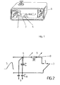
- the burst generator in Fig. 1 continuously generates burst pulses different amplitude.
- the height of the amplitude is statistically evenly distributed.
- a Switch 1 With a Switch 1, the steepness of the burst pulses can be switched.
- the optical receiver is connected to an EMC sensor by means of connection 4 via 2.2 mm plastic optical fibers.
- the received signal is displayed on LED SIGNAL 2. Pulses that are too short and therefore not visible are stretched and can be recognized by the LED SPIKE 3.
- the optical receiver is internally connected to the frequency counter.
- the frequency counter detects the burst pulses that exceed the interference threshold of the sensor in the measuring arrangement and reach the optical receiver as a light signal.
- the lower the interference threshold the more counting pulses are generated and the higher the counting result.
- the numerical value is inversely proportional to the electromagnetic compatibility of the measuring arrangement.
- the auxiliary power is provided by means of a 12 volt DC, 800 mA plug-in power supply, the display has 6 digits, the measuring time and measuring cycle are 1 second.
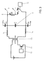
- FIG. 2 illustrates the basic structure of the interference generator according to the invention.
- a spark gap 7 is arranged whose pitch s varies according to frequency f2.
- the interference pulses 9 are decoupled either on the capacitor 6 by means of the decoupling capacitors C A or via the resistor or the network 8.
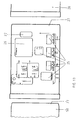
- Fig. 3 shows an embodiment variant for the circuit of the new interference generator.
- the transistor interrupter 11 is controlled by a frequency generator 12 with the frequency f 1 .
- the transistor interrupter 11 interrupts a direct current in the primary winding of the transformer 13, as a result of which a voltage pulse is induced on the secondary side of the transformer 13.
- This voltage pulse charges the capacitor 6 via the chokes 14. If the voltage across the capacitor C corresponds to the breakdown voltage of the spark gap 7, the capacitor C is suddenly discharged as a result of the breakdown of the spark gap.
- the process is decoupled from the transformer 13 with the chokes 14.
- the steepness of the discharge process of C is determined by network 8, here a resistor R. This steep voltage edge is coupled out of the circuit as an interference pulse.
- the coupling-out 9 can take place via the coupling-out capacitors C A on the capacitor C or directly on the resistor R.
- the striking distance of the spark gap s is continuously increased or decreased. This process takes place periodically with the frequency f 2 .
- a mechanically oscillating or oscillating system is used, which in the simplest case can be implemented using the contact system of a relay.
- the relay is periodically excited by the frequency generator 6 with the frequency f 2 .
- the frequency f 1 of the generator 12 is set higher than the frequency f 2 of the generator 10. Both generators 12, 10 run asynchronously, so that the amplitudes of the pulse trains are distributed virtually statistically.
- the induction loop 15 shown in Fig. 4 serves the Investigation of the magnetic component in circuits and circuit models.
- the loop is over two cables (0.64 mm socket) with the circuit model or an EMC sensor connected.
- FIG. 5 shows the magnetic field probes to be used analogously to the induction loop in the simple version according to probe A and in the more comfortable version according to probe B with a handle (housing) 18.
- the probes A and B are composed of an induction loop 15, an optical transmitter 16, which here only consists of a transmitting diode (see FIG. 5a), and a plastic optical waveguide 17.
- the optical fiber 17 of the probe is connected to the optical receiver of the burst generator / counter.
- the counter of the device determines the pulse density of the magnetic field recorded by the probe.
- the disturbance current to build up a corresponding magnetic field is generated by the burst generator.
- a fast diode Trans-Zorb
- a constant current from the constant current source 19 is superimposed on the circuit 5 a, b, c. This increases the sensitivity of the transmitter diode 16 to pulsed currents of the induction loop 15.
- a throttle L is arranged between the constant current source 19 and the pulse circuit for pulse decoupling.
- the constant current is decoupled from the induction coil by a capacitor C.
- the constant current source 19 consists of a battery with a series resistor.
- the series resistor can be adjustable for setting different currents and thus sensitivities.
- FIGS. 6 to 10 show design variants of circuit models.
- the circuit model U according to FIG. 6 is for simple studies of electrical and magnetic Influencing components provided. As coupling structures cables with a 0.64 mm socket or an induction loop 15 connected.
- the power supply takes place for all circuit models with the power supply module 28, see. also Fig. 13.
- a sensor can be plugged onto the power supply module 28, the input of which is led to a 0.64 socket connection via a plug connector.
- the interference generator can be fed through the burst generator via further sockets.
- a signal conductor 31 Arranged in the opening 23 is a signal conductor 31 which is connected on one side to the GND surface 20 and on the other side to the input of a sensor or the input of an intermediate IC.
- the signal conductor 31 arranged in the opening 23 can also be designed to be movable and thus be displaceable.
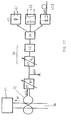
- circuit model K in Fig. 8 universal Investigations of electrical, magnetic and inductive influencing components as well as the EMC properties from IC 21.
- An EMC sensor 22 can be connected directly to the signal connection or by connecting an IC.
- the Variable GND ratios are created by insertion specially designed GND surfaces 30, see. also Fig. 11.
- circuit models G01 and G02 which are used for the universal investigation of influencing problems when connecting modules.
- the connection to another module in the case of an examination simulated by the circuit model G02 according to FIG. 9.2, is made via the header 32 and a ribbon cable 33.
- a connection to other circuit models or the power supply 28 can be established via a direct plug connector.
- the auxiliary energy for operating the module can be taken directly from 28 or fed in via the ribbon cable 33.
- circuit model I shows the circuit model I, it is used to implement the inductive influencing component.
- Essential features are the 20 mm wide GND conductor track 20, into which interference current is fed, and the grinder 24 sliding on this conductor track for tapping longitudinal voltages.
- the connection to the power supply module 28 is made by a direct connector 27.
- FIG. 11 illustrates a selection of GND areas 30 with structures with different geometries.
- All GND areas have slots for insertion, for example in the circuit model K in Fig. 8, required the same Pitch dimensions and have slide rails 29 on both sides.
- the individual structures of the applied GND grid lines allow for electrical, magnetic, and inductive component simulating different Influences. These include, for example Conductor tracks transverse and / or along the field direction of the arranged electrical and magnetic component and the interference current flowing through these structures is thereby evaluable for these concrete conditions, i.e. the Effects on the respective circuits can be measured through EMC sensors or upstream of the sensor IC or with magnetic field probes.
- the basic design of the circuit model R is shown in FIG.
- the live conductor of the supply rail 45.1 is fixed.
- the return conductor 45.2 is designed as a fixed or flexible line in order to make the position of the live conductor as variable as desired.
- the lines of the control voltage 46 and the load 47 can be connected via plug connectors or terminals 49.
- the influencing effect of switching can be determined in several ways: Once via a fixed signal conductor loop 15 with a pluggable EMC sensor 22; furthermore via circuit models 50 (K, G) which can be plugged on via a direct plug connector 27; furthermore via special sensors placed at different locations of the circuit model R or via B and E field probes.
- the relays are controlled by a signal generator SQ plugged onto circuit model R or via a direct plug connector from another circuit model.
- the interface model SM according to FIG. 13 is designed for the EMC dimensioning of signal inputs at interfaces.
- Interface circuits are implemented by plugging in components 25, for example trans-Zorb, varistors, capacitors, resistors or by connecting such internal components via DIL switches.
- the required IC sensitivity is set by plugging the corresponding EMC sensors or special components 26 (IC, optocoupler, etc.) onto an (up to 16-pin) IC adapter.
- the circuit parts with the inputs E1 / E2 are intended for investigations of fast, low-energy disturbance variables (burst), and the circuit parts with the inputs E3 / E4 are suitable for the investigation of energy-rich disturbance variables (lightning 1,2 / 50; 8/20).
- the inputs E1 / E2 can be connected to further circuit models via the socket strip of a direct plug connector 27.
- the auxiliary power supply takes place via a direct plug connector 27 from the power supply module 28 according to FIG. 14.
- the power supply module SV according to FIG. 13 ensures the galvanically isolated 5 V voltage supply of EMC sensors.
- connection to a circuit model is again made by means of a direct connector 27, through which the GND area, two sensor inputs and V cc connections are made.
- the auxiliary power is taken from a 9 V block battery.
- the quartz-stabilized signal generator SQ according to FIG. 15 is plugged onto the circuit models according to the invention. Its frequency is adjustable in 16 steps between 1 MHz and 0.05 Hz. Its duty cycle is 1: 1, it has a TTL output and the frequency is displayed by means of an LED. The pulse duty factor can be changed with an expansion module.
- the circuit model SM can be another circuit model by connecting to a direct connector be preceded.
- These circuit models can special interface models, e.g. Models, in which different types of cables, shield connection variants, Connector variants, etc. can be tested.
- the cable and device sensor used as the EMC sensor 22 is shown using a block diagram.
- the line-bound disturbance variable 35 is picked up by a detection unit 15 and its size can be changed by an assembly 37 for adjusting the electromagnetic properties. This change or adjustment corresponds to the first sensor parameter, which simulates the coupling of the device to be monitored.
- the module or circuit With the unit for the second sensor parameter 38, the IC sensitivity of the device to be monitored, the module or circuit is taken into account and the corresponding dynamic switching threshold is thus simulated.
- the pulse shaper / driver stage 39 and the downstream display / output unit 40 complete the measuring sensor. All components or assemblies are connected in series.
- Fig. 17 illustrates the cable and Device sensor with two adjustable sensor parameters using a block diagram in which all for execution of such a measurement sensor required assemblies or components are drawn.
- FIG. 18 An executed circuit based on this block diagram 17 is shown in FIG. 18.
- the induction loop 15 in the form of an eight detects the magnetic field i st caused by the interference current i st flowing through the connecting line 36 for the device 41 to be monitored.
- a voltage ⁇ U io is induced in the induction loop 15.
- the electromagnetic device properties are simulated with the induction loop.
- the loop behaves similarly to a signal conductor strip in a device circuit.
- the strength of the coupling can be varied by a voltage divider R1 (component 37).
- the voltage ⁇ U i arises, which acts on the dynamic switching threshold of an IC input (component 42).
- the series resistor R v (component 43) changes the IC sensitivity especially for bipolar IC inputs.
- the input E represents the input of an IC that has a defined dynamic switching threshold and belongs to a specific IC family.
- ⁇ U i is converted into a logic signal S.
- the logic signal is converted into a signal L of defined length by the pulse shaper 39.1.
- the logic signal S has a duration of a few ns and is extended by the pulse shaping stage 39.1 so that it can be processed further.
- the output signal of driver 39.2 can control a relay 40.2, for example.
- LED 10.1 with which the signal is directly visible on the compact measuring system / measuring sensor can be made.
- the LED display is on the Front integrated in the housing of the measuring sensor.
- Another display / output option is provided with an optocoupler or optical transmitter and fiber optic cable (module 40.3).
- Alternative components 43 for adjusting the IC sensitivity are shown in FIG. 18 by means of an IC sensitivity adjustment by raising the potential 43.1 and by means of a low-pass filter 43.2.
Landscapes
- Physics & Mathematics (AREA)
- Electromagnetism (AREA)
- General Physics & Mathematics (AREA)
- Testing Electric Properties And Detecting Electric Faults (AREA)
- Printing Elements For Providing Electric Connections Between Printed Circuits (AREA)
- Eye Examination Apparatus (AREA)
- Tests Of Electronic Circuits (AREA)
- Testing Or Calibration Of Command Recording Devices (AREA)
Description
Unter EMV-Verhalten soll dabei die geräteinterne Wandlung einer elektromagnetischen Störgröße in einen Funktionsfehler verstanden werden.
Aus dem Zeitverlauf von Meßwerten läßt sich erfahrungsgemäß nur schwer die Entscheidung ableiten, ob ein Gerät gestört ist oder nicht.
Das leitungsgebundene Eindringen ist für die Entstehung von Störgrößen und Funktionsfehlern dominierend. Bei den meisten Geräten ist nur ein leitungsgebundenes Eindringen möglich. Selbst wenn Störgrößen über das im Raum wirkende Feld eindringen, fließen sie als Störstrom durch die Schaltungen hindurch und über Leitungsverbindungen ab und können im Inneren auf den Schaltungen oder an den Zuführungs-Leitungen erfaßt werden.
Diese Impulse können ohne Probleme über galvanische Trennstellen an die Geräteschnittstelle gelangen und in das Gerät eindringen. Sie fließen über die parasitären Kapazitäten (einige pF) der galvanischen Trennstellen und weiter über induktivitätsarme Leitungen der Geräteschaltung.
Weiterhin kann der Störstrom ein Magnetfeld erzeugen, das in Schleifen, die von Signalleiterzügen und Masseleitungen bzw. von speziellen GND-Strukturen gebildet werden, Spannungen induziert. Diese Spannungen liegen ebenfalls an den IC-Eingängen an und werden als magnetische Komponente bezeichnet.
Darüberhinaus kann durch Störspannungsdifferenzen zum Signalleiterzug noch eine elektrische Komponente entstehen.
Alle drei Komponenten erzeugen an den IC-Eingängen eine Störspannung.
Der Aufbau des Burstgenerators/Zählers ist auf das Experimentieren mit EMV-Sensoren zugeschnitten. Er vereinigt die für das Impulsdichteverfahren notwendigen drei Einzelgeräte Burstgenerator, Optischer Empfänger und Frequenzzähler in einem Gerät.
Beim Impulsdichteverfahren nach der DE-A-42 24 858 erzeugt ein Burstgenerator während der Zykluszeit T eine Burstimpulsfolge steigender Amplitude. Diese Burstimpulsfolge wird in ein Gerät, eine Baugruppe oder Schaltung eingekoppelt.
Eine Signalleitung wird mit dem EMV-Sensor verbunden. Bei überschreiten der dynamischen Störschwelle gibt der Sensor ein Signal ab. Das Signal wird zur Entkopplung über einen Lichtwellenleiter (LWL) geführt und zählt einen Frequenzzähler einen Schritt weiter. Der Frequenzzähler kann nur diejenigen Impulse des Störgenerators zählen, die die Störschwelle der Schaltung überschreiten. Die Impulszahl ist der Störschwelle umgekehrt proportional.
Das Impulsdichteverfahren ermöglicht die unkomplizierte Erfassung von Verträglichkeitsänderungen in einer Meßzeit von etwa einer Sekunde.
Der Burstgenerator besteht aus einem Kondensator C, der mit einem Hochspannungsimpuls der Frequenz f1 periodisch aufgeladen wird.
Parallel zum Kondensator C befindet sich eine in ihrer Schlagweite s mit der Frequenz f2 veränderliche Funkenstrecke.
Die Entladung der Funkenstrecke erfolgt über das Netzwerk R, das im einfachsten Fall aus einer R-L-Kombination oder auch nur aus einem Widerstand besteht. Mit diesem Netzwerk kann die Impulsform der Entladung beeinflußt werden. Die Entladung selbst wird als Störimpuls am Ausgang des
Generators ausgekoppelt. Die Auskopplung erfolgt dabei am Netzwerk R oder am Kondensator C.
Die Spannungsimpulserzeugung und die periodische Schlagweitenveränderung erfolgen vorzugsweise mit unterschiedlicher Frequenz. Generell kann jedoch die Funkenstrecke mit ihrer Frequenz f2 synchron oder asysnchron zu den Hochspannungsimpulsen der Frequenz f1 schwingen. Ein asynchrones Schwingen bewirkt jedoch eine größere Amplitudenvielfalt.
Das pendelnde öffnen und Schließen kann durch ein schwingendes mechanisches System erzeugt werden, das hohe Schaltgeschwindigkeiten erreicht.
Der einzelne Impuls zündet dabei in das schwingende Kontaktsystem der Funkenstrecke hinein und findet hier eine jeweils unterschiedliche Schlagweite s(t) vor. Diese unterschiedliche Schlagweite führt wiederum zu der gewünschten unterschiedlichen Durchschlagspannung und damit zur Generierung einer für die Meßaufgabe erforderlichen Störamplitudenfolge.
Analog zur Induktionsschleife können auch Magnetfeldsonden eingesetzt werden. In der Grundkonfiguration besteht eine derartige Magnetfeldsonde aus einer Induktionsschleife, einem optischem Sender und einem Lichtwellenleiter. Zum Betreiben der Sonde ist keine Hilfsenergie erforderlich.
Die Sonde erfaßt Burstmagnetfelder hoher Flankensteilheit und wurde für die Anwendung des Impulsdichteverfahrens konzipiert.
Das Schaltungsmodell U dient einfachen Untersuchungen der elektrischen und magnetischen Beeinflussungskomponenten.
Als Einkoppelstrukturen lassen sich Leitungen oder eine Induktionsschleife anschließen.
Auf der Signalverbindung können bestimmte logische Pegel über Steckbrücken oder durch Aufstecken eines Signalgenerators erzeugt werden.
Steckbrücken dienen auch der Verbindung des IC und Referenz-IC mit dem Schaltungszentrum.
Die Längsspannungen werden an den Eingang eines EMV-Sensors oder zwischengeschalteten IC geführt.
Auf das Schaltungsmodell R sind Schaltkontakte, Schalter oder Relais aufsteckbar. Das Kontaktsystem der Schaltkontakte, Schalter oder Relais schaltet eine über Versorgungsschienen geführte Steuerspannung auf eine Lastleitung. Die Versorgungschiene besteht aus spannungsführendem Leiter und Rückleiter. An den beiden Enden der Versorgungschiene befinden sich Verbindungs- und Beschaltungsfelder (VBF), die auf der einen Seite eine Verbindung zur Zuführung der Steuerspannung herstellen und auf der anderen Seite eine Verbindung zum Relais und der Last.
Der Steuerstromkreis ist in den VBF mit Entstörbauelementen beschaltbar.
Die für den Steuerstromkreis aktiven Versorgungsschienen (spannungsführender Leiter und Rückleiter) können in ihrem Abstand variiert werden.
Die vom Schaltungsmodell R erzeugten Störgrößen und Beeinflussungsvorgänge werden zur Beaufschlagung anderer Teile des Meß- und Experimentiersystems genutzt.
Das PC-Modul übernimmt dabei die Verbindung zum PC. Das PC-Modul kann die Sensorsignale vorverarbeiten und den PC mit speziellen logischen Strukturen bezüglich der Echtzeitverarbeitung aller aufzunehmenden und abzugebenden Signale unterstützen.
Die Lichtwellenleiter der EMV-Sensoren werden zum PC-Modul geführt; die Signale werden von optischen Empfängern aufgenommen, vorverarbeitet und über das PC-Modul an den PC übertragen.
Schaltungsmodelle bzw. Prüflinge können durch den PC über das PC-Modul gesteuert werden. Dafür sind spezielle optoelektrische Wandler vorgesehen, die Lichtsignale in elektrische Signale wandeln. Diese Wandler werden auf dem Schaltungsmodell bzw. Prüfling angeordnet.
Im Wandler wird das Lichtsignal in ein äquivalentes digitales elektrisches Signal gewandelt und dem Signalausgang über einen Treiber zugeführt. Der Signalausgang ist umschaltbar zwischen offenem Kollektor und TTL-Ausgang. Eine LED-Anzeige signalisiert den aktiven bzw. inaktiven Zustand des Signalausgangs.
Dieser Kabel- und Gerätesensor läßt sich auf Schaltungsmodellen oder in elektronischen Geräten analog dem EMV-Sensor oder einem Sensor mit vorgeschaltetem IC einsetzen.
Er besitzt ebenfalls einen Eingang mit definierter Empfindlichkeit.
Die Kopplung charakterisiert die Eindringfähigkeit von impulsartigen Störgrößen von den Geräteschnittstellen bis zu den IC-Eingängen.
Dieser Wirkungsweg unterteilt sich in zwei Wegabschnitte, die geometrische Komponente der physischen Robustheit und in die Komponente der IC-Empfindlichkeit. Die geometrische Komponente umfaßt den Bereich vom Eintritt der Störgröße in die Geräteschaltung bis hin zur Wandlung in eine an einem IC-Eingang anliegende Störspannung. Dieser Wandlungsweg ist hauptsächlich von der Geometrie der leitfähigen Teile der Hardwareanordnung abhängig und wird deshalb als geometrische Komponente bezeichnet.
Dieser gesamte Weg läßt sich als erster Einstellparameter definieren. Er wird als Kopplung bezeichnet.
Die Kenngröße Empfindlichkeit beinhaltet die Wandlungsfähigkeit einer Störspannung in ein logisches Signal durch ein logisches Element. Das logische Signal kann in der logischen Struktur der Schaltung weiterverarbeitet werden und letztlich zu Funktionsfehlern führen. An den Wirkungsweg des Störvorganges, der durch die physische Robustheit beschrieben wird, schließt sich der Wirkungsweg der logischen Robustheit an. Die logische Robustheit verhindert mit logischen Mitteln, daß das über die physische Robustheit vermittelte Störsignal (logisches Signal) sich in Funktionsfehler wandelt.
Die Schleife kann alternativ in einem kompakt ausgeführten Kabel- und Gerätesensor fest eingebaut sein. Sie kann über Steckverbinder von außen aufsteckbar sein (Modul), oder über Steckverbinder kann der Kabel- und Gerätesensor mit geräteinternen Leiterschleifen (Leiterkarte des Prüflings) verbunden werden.
Eine Platte des Kondensators kann von den leitfähigen Teilen des Gerätes der Baugruppe oder der Schaltung gebildet werden.
Der Plattenkondensator kann intern oder extern über Steckverbinder an den Kabel- und Gerätesensor angeschlossen sein.
Die IC-Empfindlichkeitsverstellung erfolgt durch solche Maßnahmen, wie Verringerung der statischen und dynamischen Schaltschwelle durch Potentialanhebung bzw. Stromüberlagerung oder Erhöhung der dynamischen Schaltschwelle durch Tiefpaßeinsatz.
Die Anwendung kann an Schaltungsmodellen des Meß- und Experimentiersystems oder auch an originalen Geräten oder Schaltungen erfolgen. Vorzugsweise wird für diesen Anwendungsfall der Sensor mit einer zusätzlichen Verstellmöglichkeit der Empfindlichkeit ausgerüstet, die eine lupenartige Feineinstellung ermöglicht.
- Fig. 1
- die Gesamtansicht des Burstgenerators/Zählers,
- Fig. 2
- den prinzipiellen Aufbau des Störgenerators,
- Fig. 3
- eine Schaltungsvariante des Störgenerators,
- Fig. 4
- die Induktionsschleife, als Modul ausgeführt,
- Fig. 5
- Magnetfeldsonden mit Angabe der möglichen Schaltungen,
- Fig. 6
- eine Ausführung des Schaltungsmodells U,
- Fig. 7
- eine Ausführung des Schaltungsmodells M,
- Fig. 8
- eine Ausführung des Schaltungsmodells K,
- Fig. 9
- eine Ausführung der Schaltungsmodelle G01 und G02,
- Fig. 10
- eine Ausführung des Schaltungsmodells I,
- Fig. 11
- eine Auswahl geometrischer Gestaltungsvarianten für GND-Flächen,
- Fig. 12
- eine Ausführung des Schaltungsmodells R,
- Fig. 13
- eine Ausführungsform des Schnittstellenmodells SM,
- Fig. 14
- den Stromversorgungsbaustein SV,
- Fig. 15
- die schematische Darstellung eines Signalgenerators SQ,
- Fig. 16
- Blockschaltbild des Kabel- und Gerätesensors,
- Fig. 17
- Blockschaltbild des Meßsensors mit Angabe aller Baugruppen,
- Fig. 18
- ausgeführte Schaltung auf der Grundlage des Blockschaltbildes nach Fig. 17.
Das empfangene Signal wird an der LED SIGNAL 2 angezeigt.
Zu kurze und deshalb nicht sichtbare Impulse werden gedehnt und sind an der LED SPIKE 3 erkennbar. Der Optische Empfänger ist intern mit dem Frequenzzähler verbunden.
Die Hilfsenergie wird mittels Steckernetzteil 12 Volt DC, 800 mA bereitgestellt, die Anzeige ist 6-stellig, Meßzeit und Meßzyklus betragen 1 Sekunde.
Dieser Spannungsimpuls lädt über die Drosseln 14 den Kondensator 6 auf. Wenn die Spannung am Kondensator C der Durchschlagspannung der Funkenstrecke 7 entspricht, wird infolge des Durchschlagens der Funkenstrecke der Kondensator C schlagartig entladen. Mit den Drosseln 14 wird der Vorgang vom Trafo 13 entkoppelt. Die Steilheit des Entladevorganges von C wird vom Netzwerk 8, hier ein Widerstand R, bestimmt. Diese steile Spannungsflanke wird als Störimpuls aus der Schaltung ausgekoppelt. Die Auskopplung 9 kann über die Auskoppelkondensatoren CA am Kondensator C erfolgen oder direkt am Widerstand R.
Die Frequenz f1 des Generators 12 ist höher als die Frequenz f2 des Generators 10 eingestellt.
Beide Generatoren 12, 10 laufen asynchron, so daß die Amplituden der Impulsfolgen quasi statistisch verteilt sind.
Der Lichtwellenleiter 17 der Sonde wird mit dem optischen Empfänger des Burstgenerators/Zählers verbunden. Der Zähler des Gerätes ermittelt die Impulsdichte des von der Sonde aufgenommenen Magnetfeldes. Der Störstrom zum Aufbau eines entsprechenden Magnetfeldes wird vom Burstgenerator erzeugt.
In der angegebenen Schaltung nach 5b und 5c ist als Stoßspannungsbegrenzer eine schnelle Diode (Trans-Zorb) parallel geschaltet.
Die Konstantstromquelle 19 besteht im einfachsten Fall aus einer Batterie mit einem Vorwiderstand. Der Vorwiderstand kann zur Einstellung verschiedener Ströme und damit Empfindlicheiten verstellbar sein.
Ein Sensor kann auf den Stromversorgungsbaustein 28 aufgesteckt sein, dessen Eingang über einen Steckverbinder auf einen 0,64 Buchsenanschluß geführt ist. Über weitere Buchsen läßt sich die Störstromeinspeisung durch den Burstgenerator vornehmen.
Der in der Öffnung 23 angeordnete Signalleiterzug 31 kann auch beweglich ausgeführt und damit verschiebbar sein.
Die Verbindung zu einer anderen Baugruppe, im Untersuchungsfall nachgebildet durch das Schaltungsmodell G02 nach Fig. 9.2 erfolgt über die Pfostenleiste 32 und eine Bandleitung 33.
Beim Schaltungsmodell G02 nach Fig. 9.2 kann über einen direkten Steckverbinder eine Verbindung mit anderen Schaltungsmodellen oder der Stromversorgung 28 hergestellt werden. Die Hilfsenergie zum Betreiben der Baugruppe kann direkt aus 28 entnommen oder über die Bandleitung 33 eingespeist werden.
Wesentliche Merkmale sind der 20 mm breite GND-Leiterzug 20, in den Störstrom eingespeist wird, und der auf diesem Leiterzug gleitende Schleifer 24 zum Abgreifen von Längsspannungen.
Die Verbindung mit dem Stromversorgungsbaustein 28 erfolgt durch einen direkten Steckverbinder 27.
Auf dem Schaltungsmodell befinden sich Buchsen zum Aufstecken von Relais 44, Verbindungs- und Beschaltungsfelder (VBF) 48 auf der Einspeiseseite und der Relaisseite dienen der Verbindung der Versorgungsschienen 45 und der Aufnahme von Beschaltungselementen (Entstörkondensatoren, Varistoren, ...). Der spannungsführende Leiter der Versorgungsschiene 45.1 ist fest angeordnet. Der Rückleiter 45.2 ist fest oder flexibel als Leitung ausgeführt, um die Lage zum spannungsführenden Leiter beliebig veränderlich zu gestalten.
Über Steckverbinder bzw. Klemmen 49 können die Leitungen der Steuerspannung 46 und die Last 47 angeschlossen werden.
Einmal über eine fest angeordnete Signalleiterschleife 15 mit aufsteckbarem EMV-Sensor 22; weiterhin über Schaltungsmodelle 50 (K, G), die über einen direkten Steckverbinder 27 ansteckbar sind; des weiteren über spezielle an verschiedenen Orten des Schaltungsmodelles R plazierte Sensoren oder über B- und E-Feldsonden.
Die Steuerung der Relais erfolgt durch einen auf das Schaltungsmodell R aufgesteckten Signalgenerator SQ oder über einen direkten Steckverbinder aus einem anderen Schaltungsmodell.
Die Einstellung der erforderlichen IC-Empfindlichkeit erfolgt durch Aufstecken entsprechender EMV-Sensoren oder spezieller Bauelemente 26 (IC, Optokoppler usw.) auf einen (bis 16poligen) IC-Adapter.
Die Schaltungsteile mit den Eingängen E1/E2 sind für Untersuchungen schneller, energiearmer Störgrößen (Burst) vorgesehen, und die Schaltungsteile mit den Eingängen E3/E4 sind für die Untersuchung energiereicher Störgrößen (Blitz 1,2/50; 8/20) geeignet. Die Eingänge E1/E2 sind über die Buchsenleiste eines direkten Steckverbinders 27 mit weiteren Schaltungsmodellen verbindbar.
Der Stromversorgungsbaustein SV nach Fig. 13 gewährleistet die galvanisch getrennte 5 V-Spannungsversorgung von EMV-Sensoren.
Die Hilfsenergie wird von einer 9 V Block-Batterie entnommen.
Der quarzstabilisierte Signalgenerator SQ nach Fig. 15 wird auf den erfindungsgemäßen Schaltungsmodellen aufgesteckt.
Seine Frequenz ist in 16 Stufen zwischen 1 MHZ und 0,05 HZ verstellbar. Sein Tastverhältnis ist 1 : 1, er besitzt einen TTL-Ausgang und die Frequenzanzeige erfolgt mittels LED.
Mit einem Erweiterungsbaustein ist das Tastverhältnis veränderbar.
Die leitungsgebundene Störgröße 35 wird von einer Erfassungseinheit 15 aufgenommen und kann in ihrer Größe durch eine Baugruppe 37 zur Verstellung der elektromagnetischen Eigenschaften verändert werden. Diese Veränderung bzw. Verstellung entspricht dabei dem ersten Sensorparameter, der die Kopplung des zu überwachenden Gerätes nachbildet.
Alle Bauelemente bzw. Baugruppen sind in Reihe geschaltet.
In der Induktionsschleife 15 wird eine Spannung ΔUio induziert. Mit der Induktionsschleife werden die elektromagnetischen Geräteeigenschaften nachgebildet. Die Schleife verhält sich ähnlich wie ein Signalleiterzug in einer Geräteschaltung. Die Stärke der Kopplung läßt sich durch einen Spannungsteiler R1 (Bauelement 37) variieren.
Es entsteht die Spannung ΔUi, die auf die dynamische Schaltschwelle eines IC-Eingangs (Bauelement 42) wirkt.
Das Ausgangssignal des Treibers 39.2 kann z.B. ein Relais 40.2 ansteuern.
Alternative Bauelemente 43 zur Verstellung der IC-Empfindlichkeit sind in Fig. 18 mittels einer IC-Empfindlichkeitsverstellung durch Potentialanhebung 43.1 sowie durch Tiefpaß 43.2 dargestellt.
Claims (26)
- Meß- und Experimentiersystem zur Erfassung und Bewertung des EMV-Verhaltens elektrischer Geräte, Baugruppen und Schaltungen auf der Basis des geräteinternen Wandlungsmechnismus von Störgrößen in logische Veränderungen, wobei das erzeugte Störsignal bei Überschreiten einer Schaltschwelle, die auf die Empfindlichkeit der in der Schaltung verwendeten IC's (21, 42) und EMV-Sensoren (22) abgestimmt ist, ein logisches Signal erzeugt,
dadurch gekennzeichnet, daß zur Erzeugung konkreter Beeinflussungssituationen folgende Module bzw. Funktionsbausteine im Meß- und Experimentiersystem verknüpft sindBurstgenerator/Zähler,Induktionsschleife (15) oder Magnetfeldsonde,Schaltungsmodell U zur Untersuchung der elektrischen und magnetischen Beeinflussungskomponenten,Schaltungsmodell M zur Untersuchung magnetisch wirksamer Öffnungen (23) in GND-Flächen (20),Schaltungsmodell K für universelle Untersuchungen der elektrischen, magnetischen und induktiven Beeinflussungskomponenten und der EMV-Eigenschaften von IC (21),GND-Flächen (30) zum Einschieben in die dafür vorgesehenen Schaltungsmodelle,Schaltungsmodell G01 und G02 zur universellen Untersuchung von Beeinflussungsproblemen bei der Verbindung von Geräten, Baugruppen und SchaltungenSchaltungsmodell I zur Realisierung der induktiven Beeinflussungskomponente,Schaltungsmodell R zur Untersuchung von Störgrößen und Beeinflussungsvorgängen, die durch schaltende Kontakte hervorgerufen werden,Schnittstellenmodell SM zur EMV-Dimensionierung von Signaleingängen an Schnittstellen,optoelektronischer Wandler mit Lichtwellenleitereingang und TTL-, offenen Kollektor- oder Relaisausgang,Stromversorgungsbaustein SV zur galvanisch getrennten 5 V Spannungsversorgung von Schaltungsmodellen bzw. EMV-Sensoren,quarzstabilisierter Signalgenerator zum Aufstecken auf die eingesetzten Schaltungsmodelle,PC-Modul,EMV-Sensor in der Ausführung als aufsteckbarer Miniatursensor (22) mit feststehender Empfindlichkeit und Kopplung sowie als Kabel- und Gerätesensor. - Meß- und Experimentiersystem nach Anspruch 1,
dadurch gekennzeichnet, daß der Burstgenerator/Zähler die für das Impulsdichteverfahren notwendigen drei Einzelfunktionen Burstgenerator, Optischer Empfänger (4) und Frequenzzähler in einem Gerät beinhaltet, wobei die Steilheit der Burstimpulse verstellbar ist, der Optische Empfänger über einen Lichtwellenleiter mit einem EMV-Sensor sowie intern mit dem Frequenzzähler verbunden ist. - Meß- und Experimentiersystem nach Anspruch 1,
dadurch gekennzeichnet, daß der Störgenerator aus einem mit Hochspannungsimpulsen (5) der Frequenz f1 periodisch aufgeladenen Kondensator C (6) besteht und parallel zu diesem Kondensator eine in ihrer Schlagweite s nach der Frequenz f2 periodisch veränderliche Funkenstrecke (7) angeordnet ist, wobeidie Funkenstrecke (7) über ein mit der Frequenz f2 schwingendes und in seiner Frequenz steuerbares mechanisches System verfügt, das eine pendelnde oder rotierende Bewegung der Kontakte der Funkenstrecke bewirkt,sich die Schlagweite s der Funkenstrecke (7) nach einer bestimmten Zeitfunktion verändert,die Entladung der Funkenstrecke (7) über das Netzwerk R (8) erfolgt,mit dem Netzwerk R die Impulsform der Entladung veränderbar ist,die Auskopplung der Störimpulse (9) über den Kondensator (6) oder das Netzwerk (8) erfolgt. - Meß- und Experimentiersystem nach Anspruch 3,
dadurch gekennzeichnet, daß als pendelndes bzw. schwingendes System der Kontakte einer Funkenstrecke (7) das Kontaktsystem eines Relais vorgesehen ist, wobei das Relais von einem Frequenzgenerator (10) mit der Frequenz f2 beaufschlagt ist. - Meß- und Experimentiersystem nach Anspruch 3,
dadurch gekennzeichnet, daß zur Ausführung einer rotierenden Bewegung der Kontakte der Funkenstrecke (7) exzentrisch geformte rotierende Kurvenscheiben vorhanden sind. - Meß- und Experimentiersystem nach Anspruch 1,
dadurch gekennzeichnet, daß die Magnetfeldsonde aus einer Induktionsschleife (15), einem optischen Sender (16) und einem Lichtwellenleiter (17) besteht, wobei die Schleife (15) flexibel als Kabel oder als starres Formelement ausgeführt ist. - Meß- und Experimentiersystem nach Anspruch 6,
dadurch gekennzeichnet, daß zur Erhöhung und zur Regulierung der Empfindlichkeit der Sonde eine Konstantstromquelle (19) vorhanden ist, wobei der Konstantstrom in der Sendediode (16) dem Strom der Induktionsschleife (15) überlagert ist. - Meß- und Experimentiersystem nach Anspruch 6 oder 7,
dadurch gekennzeichnet, daß zur Impulsverlängerung in Reihe oder parallel zum optischen Sender (16) schnelle Dioden und zusätzlich Kondensatoren und Widerstände vorsehbar sind. - Meß- und Experimentiersystem nach Anspruch 1,
dadurch gekennzeichnet, daß bei dem Schaltungsmodell U als Einkoppelstrukturen Leitungen oder die Induktionsschleife (15) angeschlossen sind. - Meß- und Experimentiersystem nach Anspruch 1,
dadurch gekennzeichnet, daß bei dem Schaltungsmodell M zur Abdeckung der im Schaltungsmodell befindlichen Öffnung (23) GND-Flächen (30) einer vorgegebenen Geometrie eingesetzt sind und das Schaltungsmodell einen Signalleiterzug (31) besitzt. - Meß- und Experimentiersystem nach Anspruch 1,
dadurch gekennzeichnet, daß beim Schaltungsmodell K durch Einschieben unterschiedlicher GND-Flächen (30) zwischen zwei IC (21) unterschiedliche Beeinflussungsbedingungen für die Signalverbindung nachgebildet sind, wobei IC mit bestimmten Eingangs- und Ausgangseigenschaften auf Fassungen aufsteckbar sind und ein EMV-Sensor (22) direkt an die Signalverbindung, oder durch Zwischenschalten eines IC angeschaltet ist. - Meß- und Experimentiersystem nach Anspruch 11,
dadurch gekennzeichnet, daß auf der Signalverbindung bestimmte logische Pegel über Steckbrücken oder durch Aufstecken eines Signalgenerators realisierbar sind. - Meß- und Experimentiersystem nach Anspruch 10 oder 11,
dadurch gekennzeichnet, daß auf den GND-Flächen (30) gleichen Rasters bestimmte geometrische GND-Strukturen realisiert sind. - Meß- und Experimentiersystem nach Anspruch 1,
dadurch gekennzeichnet, daß mit dem Schaltungsmodell G01 bei ähnlichem Aufbau wie das Modell K eine Signalverbindung zwischen zwei IC (21) nachgebildet ist und die zu untersuchende Verbindung zu einem anderen Gerät, Baugruppe oder Schaltung durch das über eine Pfostenleiste (32) und eine Leitung (33) angeschlossene Schaltungsmodell G02 erfolgt, wobei die Pfostenleiste (32) über Signalleiterzüge (31) mit den Ein- oder Ausgängen (34) eines IC verbindbar ist. - Meß- und Experimentiersystem nach Anspruch 1,
dadurch gekennzeichnet, daß beim Schaltungsmodell I ein mit Störstrom beaufschlagter GND-Leiterzug (20) vorhanden ist, von dem mittels eines Schleifers (24) und eines mit ihm verbundenen Signalleiterzuges (31) Längsspannungen abgreifbar sind. - Meß- und Experimentiersystem nach Anspruch 1,
dadurch gekennzeichnet, daß beim Schaltungsmodell R aufsteckbare Schaltkontakte, Schalter oder Relais (44) vorhanden sind, deren Kontaktsystem eine über Versorgungschienen (45) geführte Steuerspannung (46) auf eine Lastleitung (47) schaltet, wobei an den beiden Enden der Versorgungsschienen (45) Verbindungs- und Beschaltungsfelder VBF (48) angeordnet sind, die auf der einen Seite eine Verbindung zur Zuführung der Steuerspannung (46) und auf der anderen Seite zum Relais (44) sowie zur Last (47) herstellen. - Meß- und Experimentiersystem nach Anspruch 1,
dadurch gekennzeichnet, daß beim Schnittstellenmodell SM zum Aufbau von Schnittstellenschaltungen Bauelemente (25), wie Trans-Zorb, Varistoren, Kondensatoren, Widerstände usw. aufsteckbar sind oder durch Zuschalten interner Bauelemente vorgegeben sind, wobei die erforderliche IC-Empfindlichkeit durch Aufstecken entsprechender EMV-Sensoren (22) oder spezieller Bauelemente (26), wie IC, Optokoppler usw. auf einem IC-Adapter einstellbar ist. - Meß- und Experimentiersystem nach Anspruch 1,
dadurch gekennzeichnet, daß die Verbindung des Stromversorgungsbausteines SV (28) mit einem Schaltungsmodell (50) und die Verbindung von Schaltungsmodellen untereinander über einen direkten Steckverbinder (27) erfolgt, über den zumindest die GND-Fläche und Verbindungen für die Versorgungsspannung sowie weitere Signalleitungen geführt sind. - Meß- und Experimentiersystem nach Anspruch 1,
dadurch gekennzeichnet, daß dem für die Steuerung und Auswertung der Meß- und Experimentierprozesse eingesetzten PC ein PC-Modul vorgeschaltet ist, das die von den Schaltungsmodellen, Prüflingen und EMV-Sensoren eingehenden Signale vorverarbeitet, den PC mit speziellen logischen Strukturen bezüglich der Echtzeitverarbeitung aller aufzunehmenden und abzugebenden Signale unterstützt und die Steuerung des Burstgenerators und der Schaltungsmodelle bzw. Prüflinge durchführt. - Meß- und Experimentiersystem nach Anspruch 1,
dadurch gekennzeichnetf, daß als EMV-Sensor (22) ein Kabel- und Gerätesensor eingesetzt wird, der die Empfindlichkeit von elektrischen Geräten, Baugruppen oder Schaltungen im Sinne der vorhandenen physischen Robustheit des Gerätes, der Baugruppen oder der elektronischen Schaltung nachbildet, wobei eine Sensorkomponente des Meßsystems als 1. Parameter die Kopplung und eine weitere Sensorkomponente als 2. Parameter die IC-Empfindlichkeit nachbildet und die Erfassung der Störgröße (35) durch das Meßsystem kontinuierlich oder in diskreten Schritten während einer vorgegebenen Meßzeit mittels des vom Störstrom ist erzeugten Magnetfeldes des zum Gerät (41) führenden Kabels (36) (oder im Gerät befindlicher Leitungen, Leiterzüge und leitfähiger Konstruktionsteile) und/oder über das vorhandene elektrische Feld und/oder auf induktivem Weg durch Auswertung des an der Induktivität des Kabels oder der Leitung (36) erzeugten Spannungsabfalls erfolgt. - Meß- und Experimentiersystem nach Anspruch 20,
dadurch gekennzeichnet, daß der 1. Sensorparameter, der die Kopplung der Schaltung, der Baugruppe des elektrischen Gerätes (41) nachbildet, durch eine Erfassungseinheit (15) für die Störgröße (35) und eine Baugruppe (37) zur Verstellung der elektromagnetischen Eigenschaften und der 2. Sensorparameter durch eine Einheit (38) zur Nachbildung und Verstellung der IC-Empfindlichkeit realisiert ist, wobei der Reihenschaltung dieser Funktionseinheiten (15, 37, 38) eine Impulsformer-/Treiberstufe (37) sowie eine Anzeige- und/oder Ausgabeeinheit (40) nachgeschaltet sind. - Meß- und Experimentiersystem nach Anspruch 21,
dadurch gekennzeichnet, daß die IC-Empfindlichkeit des Kabel- und Gerätesensors in diskreten Schritten durch Austausch von IC-Steckmodulen definierter Empfindlichkeit veränderlich ist. - Meß- und Experimentiersystem nach Anspruch 21 oder 22,
dadurch gekennzeichnet, daß die Induktionsschleife (15) in einen kompakt ausgeführten Kabel- und Gerätesensor fest eingebaut ist, oder über Steckverbinder von außen aufsteckbar ist, oder über Steckverbinder der Kabel- und Gerätesensor mit geräteinternen Leiterschleifen verbunden ist. - Meß- und Experimentiersystem nach einem der Ansprüche 21 bis 23,
dadurch gekennzeichnet, daß als Erfassungseinrichtung (15) ein elektrisch leitfähiges Plattenpaar zur Erfassung der elektrischen Komponente verhanden ist und das Plattenpaar analog einem Plattenkondensator aufgebaut ist, wobei sich die Platten gegenüber stehen oder in gestreckter Ausführung in einer Ebene neben- bzw. hintereinander angeordnet sind, und eine Platte des Kondensators von den leitfähigen Teilen des Gerätes, der Baugruppe oder der Schaltung gebildet werden kann. - Meß- und Experimentiersystem nach einem der Ansprüche 22 bis 24,
dadurch gekennzeichnet, daß als Baugruppe (37) zur Verstellung der elektromagnetischen Geräteeigenschaften ein Spannungsteiler R1 vorgesehen ist, der der Induktionsschleife (15) nachgeschaltet ist. - Meß- und Experimentiersystem nach einem der Ansprüche 22 bis 25,
dadurch gekennzeichnet, daß die Einheit (38) zur Berücksichtigung bzw. Verstellung der IC-Empfindlichkeit durch einen IC (42) und eine Schaltung zur Verringerung der statischen und dynamischen Schaltschwelle durch Potentialanhebung bzw. Stromüberlagerung oder Erhöhung der dynamischen Schaltschwelle durch Tiefpaßeinsatz dem Eingang E des IC vorgeschaltet ist.
Applications Claiming Priority (6)
| Application Number | Priority Date | Filing Date | Title |
|---|---|---|---|
| DE4330345 | 1993-09-08 | ||
| DE19934330345 DE4330345C1 (de) | 1993-09-08 | 1993-09-08 | Verfahren und Vorrichtung zur Erfassung und Bewertung des EMV-Verhaltens eines elektrischen Gerätes |
| DE9317586U DE9317586U1 (de) | 1993-11-18 | 1993-11-18 | Meß- und Experimentiersystem zur Erfassung und Bewertung des EMV-Verhaltens elektrischer Schaltungen oder Geräte |
| DE9317586U | 1993-11-18 | ||
| DE19934340514 DE4340514C2 (de) | 1993-11-27 | 1993-11-27 | Störgenerator für EMV-Meßanordnungen |
| DE4340514 | 1993-11-27 |
Publications (2)
| Publication Number | Publication Date |
|---|---|
| EP0642028A1 EP0642028A1 (de) | 1995-03-08 |
| EP0642028B1 true EP0642028B1 (de) | 1999-05-26 |
Family
ID=27205530
Family Applications (1)
| Application Number | Title | Priority Date | Filing Date |
|---|---|---|---|
| EP94113567A Expired - Lifetime EP0642028B1 (de) | 1993-09-08 | 1994-08-31 | Mess- und Experimentiersystem zur Erfassung und Bewertung des EMV-Verhaltens elektrischer Geräte, Baugruppen und Schaltungen |
Country Status (3)
| Country | Link |
|---|---|
| EP (1) | EP0642028B1 (de) |
| AT (1) | ATE180574T1 (de) |
| DE (1) | DE59408305D1 (de) |
Cited By (1)
| Publication number | Priority date | Publication date | Assignee | Title |
|---|---|---|---|---|
| CN104008246A (zh) * | 2014-06-04 | 2014-08-27 | 北京航空航天大学 | 基于矢量拟合与平衡截断法的电磁兼容宏模型建模方法 |
Families Citing this family (14)
| Publication number | Priority date | Publication date | Assignee | Title |
|---|---|---|---|---|
| ES2188408B1 (es) * | 2001-10-30 | 2004-10-16 | Fundacion Labein | Sistema de prediccion de las emisiones radiadas por un equipo electronico. |
| CN102565587B (zh) * | 2012-01-11 | 2013-12-25 | 陕西电力科学研究院 | 一种电子式互感器电磁兼容性的试验方法 |
| CN102737145B (zh) * | 2012-06-07 | 2014-03-26 | 北京航空航天大学 | 基于测量的电子元器件电磁发射宽带行为级预测建模方法 |
| CN103235210B (zh) * | 2013-04-01 | 2015-07-29 | 中国舰船研究设计中心 | 局部阵面替代满阵面的空间电磁耦合模拟实验方法 |
| WO2015015365A1 (en) * | 2013-07-31 | 2015-02-05 | Manohar Alfred | An electricity theft deterrent system and a method thereof |
| CN110045199B (zh) * | 2019-03-20 | 2024-05-03 | 杭州通鉴科技有限公司 | 一种eft/esd/cs电磁干扰分析仪 |
| CN112444722B (zh) * | 2019-08-30 | 2024-04-16 | 宁德时代新能源科技股份有限公司 | 一种电控制器件的检测电路及检测方法 |
| CN111398776B (zh) * | 2020-02-24 | 2024-07-26 | 浙江诺益科技有限公司 | 集成电路电磁发生干扰分析仪 |
| CN112834843B (zh) * | 2020-12-31 | 2023-12-19 | 江苏南高智能装备创新中心有限公司 | 一种射频集成电路近场电磁兼容性测试管理方法和系统 |
| CN114200371B (zh) * | 2021-08-09 | 2023-07-11 | 威凯检测技术有限公司 | 一种用于静电放电抗扰度试验的能力验证装置 |
| CN116068385A (zh) * | 2021-11-02 | 2023-05-05 | 中兴通讯股份有限公司 | 抗扰测试切换开关、抗扰测试系统、测试方法和存储介质 |
| CN114487661B (zh) * | 2022-01-10 | 2022-12-02 | 北京航空航天大学 | 一种基于典型电路的电磁环境适应性边界测试系统 |
| CN115494821B (zh) * | 2022-08-26 | 2024-04-12 | 南京航空航天大学 | 一种发动机控制器电路强电磁脉冲防护设计方法 |
| CN116223952A (zh) * | 2023-03-08 | 2023-06-06 | 江南机电设计研究所 | 一种设备电磁脉冲敏感边界测试系统和方法 |
Family Cites Families (2)
| Publication number | Priority date | Publication date | Assignee | Title |
|---|---|---|---|---|
| US3943296A (en) * | 1974-08-02 | 1976-03-09 | Bell Telephone Laboratories Incorporated | Method and apparatus for reducing noise in pam time division networks |
| US4071780A (en) * | 1976-09-10 | 1978-01-31 | Corcom, Inc. | Transient generator |
-
1994
- 1994-08-31 EP EP94113567A patent/EP0642028B1/de not_active Expired - Lifetime
- 1994-08-31 AT AT94113567T patent/ATE180574T1/de active
- 1994-08-31 DE DE59408305T patent/DE59408305D1/de not_active Expired - Fee Related
Cited By (1)
| Publication number | Priority date | Publication date | Assignee | Title |
|---|---|---|---|---|
| CN104008246A (zh) * | 2014-06-04 | 2014-08-27 | 北京航空航天大学 | 基于矢量拟合与平衡截断法的电磁兼容宏模型建模方法 |
Also Published As
| Publication number | Publication date |
|---|---|
| DE59408305D1 (de) | 1999-07-01 |
| EP0642028A1 (de) | 1995-03-08 |
| ATE180574T1 (de) | 1999-06-15 |
Similar Documents
| Publication | Publication Date | Title |
|---|---|---|
| EP0642028A1 (de) | Mess- und Experimentiersystem zur Erfassung und Bewertung des EMV-Verhaltens elektrischer Geräte, Baugruppen und Schaltungen | |
| DE4123725C2 (de) | Vorrichtung zum Prüfen der Isolierung eines elektrischen Leiters auf Fehlerstellen | |
| EP0777907B1 (de) | Elektromechanisches schaltgerät sowie anordnung mit mehreren derartigen schaltgeräten | |
| EP2623940B1 (de) | Prüfung einer Messgerätanordnung, entsprechende Messgerätanordnung und Prüfanordnung | |
| EP0240783A1 (de) | Ansprechzähler für einen Überspannungsableiter | |
| DE10305986A1 (de) | Messsystem mit intelligentem Sensorkopf für Mittel- oder Hochspannungsanlagen oder im Bergbau | |
| DE3727950A1 (de) | Vorrichtung zur durchfuehrung von spannungspruefungen und -messungen an einer mittel- oder hochspannungsschaltanlage | |
| DE102014101719A1 (de) | Plasmaschneidmaschine mit Schutzeinrichtung sowie Verfahren zum Betreiben der Plasmaschneidmaschine | |
| DE4012445C2 (de) | Verfahren zur Teilentladungsmessung und/oder -fehlerortung in Hochspannungsisolierungen unter Vor-Ort-Bedingungen und Anordnung zur Durchführung des Verfahrens | |
| DE19632457C1 (de) | Schaltungsanordnung zur Überwachung eines Sensors | |
| AT9099U1 (de) | Einrichtung zur messung des verlustfaktors | |
| DE19507809C2 (de) | Meßverfahren zur Erfassung pulsförmiger Störgrößen | |
| EP0190547B1 (de) | Ansprechzähl- und Überwachungs-Einrichtung für funkenstreckenlose Überspannungsableiter | |
| DE4330345C1 (de) | Verfahren und Vorrichtung zur Erfassung und Bewertung des EMV-Verhaltens eines elektrischen Gerätes | |
| DE9317586U1 (de) | Meß- und Experimentiersystem zur Erfassung und Bewertung des EMV-Verhaltens elektrischer Schaltungen oder Geräte | |
| EP2818877A1 (de) | Verfahren und Vorrichtung zur Ermittlung einer Gleichspannung in einem galvanisch isolierten System | |
| DE19913791C2 (de) | Vorrichtung zur Messung veränderlicher Widerstände elektrischer Kontakte, insbesondere Steckverbindungen | |
| DE19515068A1 (de) | Anordnung zur TE-Detektion in Hochspannungskabeln und in deren Verbindungselementen | |
| DE29514423U1 (de) | EMV-Kompaktsensor | |
| DE2725618C3 (de) | Vorrichtung zur Messung des Integrals einer zeitabhängigen physikalischen Größe | |
| EP0638812A2 (de) | Einrichtung zur Überwachung eines Auslösemittels eines elektrischen Betriebsmittels auf elektrische Defekte | |
| CH677287A5 (de) | ||
| DD277982A1 (de) | Anordnung zur teilentladungsmessung unter vor-ort-bedingungen | |
| EP3680678B1 (de) | Mess-system zur erfassung von störungen auf leitungen eines gerätes oder einer anlage | |
| WO1999001774A1 (de) | Diagnoseeinrichtung zur erkennung von fehlschlüssen bei einem induktiven sensor |
Legal Events
| Date | Code | Title | Description |
|---|---|---|---|
| PUAI | Public reference made under article 153(3) epc to a published international application that has entered the european phase |
Free format text: ORIGINAL CODE: 0009012 |
|
| AK | Designated contracting states |
Kind code of ref document: A1 Designated state(s): AT BE CH DE FR GB IT LI NL SE |
|
| 17P | Request for examination filed |
Effective date: 19950614 |
|
| GRAG | Despatch of communication of intention to grant |
Free format text: ORIGINAL CODE: EPIDOS AGRA |
|
| 17Q | First examination report despatched |
Effective date: 19980604 |
|
| GRAG | Despatch of communication of intention to grant |
Free format text: ORIGINAL CODE: EPIDOS AGRA |
|
| GRAH | Despatch of communication of intention to grant a patent |
Free format text: ORIGINAL CODE: EPIDOS IGRA |
|
| GRAG | Despatch of communication of intention to grant |
Free format text: ORIGINAL CODE: EPIDOS AGRA |
|
| GRAH | Despatch of communication of intention to grant a patent |
Free format text: ORIGINAL CODE: EPIDOS IGRA |
|
| GRAH | Despatch of communication of intention to grant a patent |
Free format text: ORIGINAL CODE: EPIDOS IGRA |
|
| GRAH | Despatch of communication of intention to grant a patent |
Free format text: ORIGINAL CODE: EPIDOS IGRA |
|
| GRAA | (expected) grant |
Free format text: ORIGINAL CODE: 0009210 |
|
| AK | Designated contracting states |
Kind code of ref document: B1 Designated state(s): AT BE CH DE FR GB IT LI NL SE |
|
| PG25 | Lapsed in a contracting state [announced via postgrant information from national office to epo] |
Ref country code: SE Free format text: THE PATENT HAS BEEN ANNULLED BY A DECISION OF A NATIONAL AUTHORITY Effective date: 19990526 Ref country code: NL Free format text: LAPSE BECAUSE OF FAILURE TO SUBMIT A TRANSLATION OF THE DESCRIPTION OR TO PAY THE FEE WITHIN THE PRESCRIBED TIME-LIMIT Effective date: 19990526 Ref country code: IT Free format text: LAPSE BECAUSE OF FAILURE TO SUBMIT A TRANSLATION OF THE DESCRIPTION OR TO PAY THE FEE WITHIN THE PRE;WARNING: LAPSES OF ITALIAN PATENTS WITH EFFECTIVE DATE BEFORE 2007 MAY HAVE OCCURRED AT ANY TIME BEFORE 2007. THE CORRECT EFFECTIVE DATE MAY BE DIFFERENT FROM THE ONE RECORDED.SCRIBED TIME-LIMIT Effective date: 19990526 Ref country code: GB Free format text: LAPSE BECAUSE OF FAILURE TO SUBMIT A TRANSLATION OF THE DESCRIPTION OR TO PAY THE FEE WITHIN THE PRESCRIBED TIME-LIMIT Effective date: 19990526 Ref country code: FR Free format text: LAPSE BECAUSE OF FAILURE TO SUBMIT A TRANSLATION OF THE DESCRIPTION OR TO PAY THE FEE WITHIN THE PRESCRIBED TIME-LIMIT Effective date: 19990526 |
|
| REF | Corresponds to: |
Ref document number: 180574 Country of ref document: AT Date of ref document: 19990615 Kind code of ref document: T |
|
| REG | Reference to a national code |
Ref country code: CH Ref legal event code: EP |
|
| REF | Corresponds to: |
Ref document number: 59408305 Country of ref document: DE Date of ref document: 19990701 |
|
| PG25 | Lapsed in a contracting state [announced via postgrant information from national office to epo] |
Ref country code: LI Free format text: LAPSE BECAUSE OF NON-PAYMENT OF DUE FEES Effective date: 19990831 Ref country code: CH Free format text: LAPSE BECAUSE OF NON-PAYMENT OF DUE FEES Effective date: 19990831 Ref country code: BE Free format text: LAPSE BECAUSE OF NON-PAYMENT OF DUE FEES Effective date: 19990831 Ref country code: AT Free format text: LAPSE BECAUSE OF NON-PAYMENT OF DUE FEES Effective date: 19990831 |
|
| EN | Fr: translation not filed | ||
| GBV | Gb: ep patent (uk) treated as always having been void in accordance with gb section 77(7)/1977 [no translation filed] |
Effective date: 19990526 |
|
| BERE | Be: lapsed |
Owner name: LANGER GUNTER Effective date: 19990831 |
|
| PLBE | No opposition filed within time limit |
Free format text: ORIGINAL CODE: 0009261 |
|
| STAA | Information on the status of an ep patent application or granted ep patent |
Free format text: STATUS: NO OPPOSITION FILED WITHIN TIME LIMIT |
|
| REG | Reference to a national code |
Ref country code: CH Ref legal event code: PL |
|
| 26N | No opposition filed | ||
| PGFP | Annual fee paid to national office [announced via postgrant information from national office to epo] |
Ref country code: DE Payment date: 20030821 Year of fee payment: 10 |
|
| PG25 | Lapsed in a contracting state [announced via postgrant information from national office to epo] |
Ref country code: DE Free format text: LAPSE BECAUSE OF NON-PAYMENT OF DUE FEES Effective date: 20050301 |