EP0641081B1 - Boucle à verrouillage de phase comprenant un filtre numérique - Google Patents
Boucle à verrouillage de phase comprenant un filtre numérique Download PDFInfo
- Publication number
- EP0641081B1 EP0641081B1 EP94410069A EP94410069A EP0641081B1 EP 0641081 B1 EP0641081 B1 EP 0641081B1 EP 94410069 A EP94410069 A EP 94410069A EP 94410069 A EP94410069 A EP 94410069A EP 0641081 B1 EP0641081 B1 EP 0641081B1
- Authority
- EP
- European Patent Office
- Prior art keywords
- filter
- value
- coefficient
- phase
- locked loop
- Prior art date
- Legal status (The legal status is an assumption and is not a legal conclusion. Google has not performed a legal analysis and makes no representation as to the accuracy of the status listed.)
- Expired - Lifetime
Links
Images

Classifications
-
- H—ELECTRICITY
- H03—ELECTRONIC CIRCUITRY
- H03L—AUTOMATIC CONTROL, STARTING, SYNCHRONISATION OR STABILISATION OF GENERATORS OF ELECTRONIC OSCILLATIONS OR PULSES
- H03L7/00—Automatic control of frequency or phase; Synchronisation
- H03L7/06—Automatic control of frequency or phase; Synchronisation using a reference signal applied to a frequency- or phase-locked loop
- H03L7/08—Details of the phase-locked loop
- H03L7/085—Details of the phase-locked loop concerning mainly the frequency- or phase-detection arrangement including the filtering or amplification of its output signal
- H03L7/093—Details of the phase-locked loop concerning mainly the frequency- or phase-detection arrangement including the filtering or amplification of its output signal using special filtering or amplification characteristics in the loop
-
- H—ELECTRICITY
- H03—ELECTRONIC CIRCUITRY
- H03L—AUTOMATIC CONTROL, STARTING, SYNCHRONISATION OR STABILISATION OF GENERATORS OF ELECTRONIC OSCILLATIONS OR PULSES
- H03L7/00—Automatic control of frequency or phase; Synchronisation
- H03L7/06—Automatic control of frequency or phase; Synchronisation using a reference signal applied to a frequency- or phase-locked loop
- H03L7/08—Details of the phase-locked loop
- H03L7/10—Details of the phase-locked loop for assuring initial synchronisation or for broadening the capture range
- H03L7/107—Details of the phase-locked loop for assuring initial synchronisation or for broadening the capture range using a variable transfer function for the loop, e.g. low pass filter having a variable bandwidth
- H03L7/1075—Details of the phase-locked loop for assuring initial synchronisation or for broadening the capture range using a variable transfer function for the loop, e.g. low pass filter having a variable bandwidth by changing characteristics of the loop filter, e.g. changing the gain, changing the bandwidth
Definitions
- the present invention relates to the production of a filter used in a digital phase locked loop and will be more particularly exposed in relation to applying such a phase locked loop in a carrier recovery system of a modem coupled to a telephone line.
- the input circuits of a modem determine from the analog signal received on the telephone line, once at each period of the sampling clock, a complex signal which, if the transmission was free from any defect , should correspond to an emitted symbol.
- this complex signal is applied to the input of a phase detector 1 and more particularly to a first input of a multiplier 2.
- the output of the multiplier 2 is sent to the first input of a angle measurement system 3 and at the input of a decision circuit 4.
- the other input of the angle measurement system 3 is constituted by the output of the decision circuit 4 which estimates, from stored tables , what are the phase and the amplitude of the symbol having characteristics closest to the received symbol.
- the angle measurement circuit determines the difference or angular error ⁇ k between the received symbol and the estimated symbol and uses this difference to readjust a complex oscillator or VCO 5 providing a complex signal which will be used to "demodulate” in the multiplier 2 the input signal.
- a loop filter 6 is provided between the error angle measurement system 3 and the input of the complex VCO 5.
- the filter is an integral type filter comprising a multiplier multiplying the error signal by a constant K L.
- K L the coefficient of the multiplier
- the output of the multiplier is added to the content of a register z -1 .
- a problem which arises with the filter used in this particular application and more generally in the PLL loop filters is that, during an initial operation, for example during the initial learning phase when two modem are put into communication. , you must quickly catch an error that can be significant.
- the initial correction has been made, for example while a modem is in communication, the phase is no longer likely to vary in significant proportions. Therefore, during the initial phase, we want to use a relatively high K L coefficient to ensure rapid enslavement, then, once the communication is established, reduce the K L coefficient (and more generally the K filter coefficients) to allow performing small corrections and do not take into account large instantaneous fluctuations normally corresponding to accidental parasites.
- phase-locked loops numerics in which the filter coefficients are changed between an initial high value and a higher value low normal operation.
- the present invention provides a digital phase locked loop filter numeric in which the filter coefficients are regularly decremented at each clock step between a value initial and a final value.
- the present invention provides in particular that these filter coefficients are decremented linearly at each no clock even if this linear decrement does not correspond not to a linear variation in the bandwidth of the filtered.
- the invention applies, in particular, to a filter proportional-integral numeric.
- the means for linearly decreasing a coefficient include a register containing the current value of the coefficient, means to initially load this register with a value initial, means to subtract from each clock time the content of the filter an increment, means to compare the current value of the filter to a final value, and means to interrupt the operation of the decrement system when the current value of the coefficient has reached the value minimal.
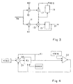
- FIG. 3 represents a digital filter of proportional-integral type which constitutes an example of a digital filter of a digital phase locked loop to which the present invention applies.
- the input of this filter receives an error signal, for example an angular error ⁇ e (called ⁇ k in Figure 1).
- This error signal is sent to two multiplier circuits 11 and 12 respectively carrying out multiplications by coefficients K1 and K2.
- the output of the multiplier 11 is sent to a first input of an adder 13 whose output is sent to a register or memory box 15.
- the output of the multiplier 12 is sent to a first input of an adder 17 whose output is looped back on its second input via a register 19 and is also sent to a second input of the adder 13.
- the output of the register 15 is applied to a third input of the adder 13.
- the input ⁇ e is for example coded on 16 bits, the output of the multipliers 11 and 12 on 32 bits and the output of the register or memory box 15 on 16 bits.
- the registers 15 and 19 are sequenced to the rhythm of the system clock, the baud clock in the case of a modem. At each clock time, registers 15 and 19 provide the value they contain and replace this value with the new value presented on their input.
- FREQ i The error integrated at a clock instant t i in the register 19 is called FREQ i , this error being able to be considered as a frequency error.
- ⁇ f i the filtered error contained in register 15 at this time.
- the values of K1 and K2 define the bandwidth of the filter.
- the present invention proposes to modify over a period determined, i.e. over a determined number of periods the bandwidth of the filter by modifying each of the coefficients K1, K2 at each clock time.
- the coefficients must be decreased at each clock time if we want to decrease the band filter bandwidth.
- FIG. 4 A process of reduction of the values of the filter coefficients K, used for each of the coefficients, is illustrated in FIG. 4.
- an initial value KMAX of a coefficient K is introduced into a register or memory box 20.
- the output of this register is sent to an adding input of a subtractor 21 whose subtraction input receives a decrement value KDEC of the coefficient K.
- Ki KMAX - i ⁇ KDEC which is applied as a coefficient input to the multiplier 11 or 12 of FIG. 3.
- the output Ki is also applied to a comparator 22 which compares this current value with a minimum value KMIN. When the value Ki reaches the value KMIN, the output of the comparator 22 inhibits the operation of the loop 20, 21 and the value Ki remains fixed at the value KMIN.
- circuit illustrated in FIG. 4 does not constitute that an example of realization of a decrementation circuit of numerical value and many other material means and / or software may be used to ensure this function.
- a linear decrement of the coefficients K1 and K2 does not necessarily result in a linear decrementation of the passband of the filter.
- the coefficient K1 in the case of a proportional-integral filter, while, to obtain a linear decrementation of the bandwidth of the filter, the coefficient K1 must actually be decremented in a linear fashion, the coefficient K2 must be decremented according to a function d 'higher order.
- K1 and K2 must be chosen respectively from 5.4.10 -2 and 1.5.10 -3 to have a filter bandwidth of the order of 10 Hz then from 3.7.10 -3 and 6.8.10 -6 to have a bandwidth on the order of 1 Hz.
- this gives the 250th clock time for K1 a value of 2.9.10 -2 and for K2 a value on the order of 4.3.10 -4 .
- the locking loop including a digital filter according to the present invention has been described in the context of a double particular case: on the one hand of a recovery loop of carrier in a modem, on the other hand of a filter of proportional-integral type.
- the present invention would apply similarly to applications to other loops (such as echo cancellation or recovery loops clock) and other filters. Note that, in separate filters, for example of higher order, it is possible that it is necessary to achieve a band reduction busy to grow and not decrease some of the filter coefficients.
- the invention will apply to such filters correspondingly, its essential aspect residing in the modification at each clock time of the coefficients filtering between an initial value and a final value.
Landscapes
- Stabilization Of Oscillater, Synchronisation, Frequency Synthesizers (AREA)
- Synchronisation In Digital Transmission Systems (AREA)
Description
Claims (5)
- Boucle à verrouillage de phase comprenant un filtre numérique recevant des signaux d'erreur dans lequel les signaux d'erreur incidents subissent au moins une multiplication par un coefficient de filtrage (K) avant d'être traités numériquement à chaque temps d'horloge pour fournir un signal filtré, caractérisé en ce qu'il comprend des moyens de décrémentation linéaire de la valeur dudit au moins un coefficient de filtrage (K) à chaque temps d'horloge pendant une période initiale de fonctionnement du filtre.
- Boucle à verrouillage de phase selon la revendication 1, caractérisé en ce que le filtre est du type proportionnel-intégral.
- Boucle à verrouillage de phase selon l'une des revendications 1 ou 2, caractérisé en ce que les valeurs initiale et finale dudit au moins un coefficient (K) sont choisies pour que le filtre ait des bandes passantes initiale et finale prédéterminées.
- Modem comportant une boucle à verrouillage de phase selon l'une quelconque des revendications 1 à 3, caractérisé en ce que la fréquence à filtrer étant la fréquence porteuse et la fréquence d'échantillonnage étant la fréquence de bauds.
- Boucle à verrouillage de phase selon la revendication 1, caractérisé en ce que les moyens de décrémentation linéaire dudit au moins un coefficient (K) comprennent :un registre (20) contenant la valeur courante (Ki) du coefficient,des moyens pour charger initialement ce registre avec une valeur initiale (KMAX),des moyens (21) pour soustraire à chaque temps d'horloge au contenu du filtre un incrément (KDEC),des moyens (22) pour comparer la valeur courante du filtre à une valeur finale (KMIN), etdes moyens pour interrompre le fonctionnement du système de décrémentation quand la valeur courante (Ki) du coefficient a atteint la valeur minimale (KMIN).
Applications Claiming Priority (2)
| Application Number | Priority Date | Filing Date | Title |
|---|---|---|---|
| FR9310578 | 1993-08-31 | ||
| FR9310578A FR2709623B1 (fr) | 1993-08-31 | 1993-08-31 | Filtre de boucle à verrouillage de phase numérique. |
Publications (2)
| Publication Number | Publication Date |
|---|---|
| EP0641081A1 EP0641081A1 (fr) | 1995-03-01 |
| EP0641081B1 true EP0641081B1 (fr) | 1999-03-03 |
Family
ID=9450589
Family Applications (1)
| Application Number | Title | Priority Date | Filing Date |
|---|---|---|---|
| EP94410069A Expired - Lifetime EP0641081B1 (fr) | 1993-08-31 | 1994-08-29 | Boucle à verrouillage de phase comprenant un filtre numérique |
Country Status (5)
| Country | Link |
|---|---|
| US (1) | US5619543A (fr) |
| EP (1) | EP0641081B1 (fr) |
| JP (1) | JPH07154247A (fr) |
| DE (1) | DE69416756T2 (fr) |
| FR (1) | FR2709623B1 (fr) |
Families Citing this family (7)
| Publication number | Priority date | Publication date | Assignee | Title |
|---|---|---|---|---|
| DE19630398C1 (de) * | 1996-07-26 | 1998-02-12 | Siemens Ag | Verfahren zum Synchronisieren eines in einer Datenempfangsstation zu generierenden Taktsignals mit einem in einer Datensendestation verwendeten Taktsignal |
| DE19630397C1 (de) * | 1996-07-26 | 1997-12-04 | Siemens Ag | Verfahren zum Erzielen einer gewünschten Solldifferenz zwischen dem Zählstand eines durch ein erstes Taktsignal zum Zählen veranlaßten ersten Zählers und dem Zählstand eines durch ein zweites Taktsignal zum Zählen veranlaßten zweiten Zählers |
| US6823133B1 (en) | 1999-11-15 | 2004-11-23 | Lexmark International, Inc. | Apparatus and method for electronic control of DC motor using an all-digital phase-locked loop |
| CN1307406A (zh) * | 2000-01-27 | 2001-08-08 | 华为技术有限公司 | 数字锁相环的滤波方法 |
| US7409028B2 (en) * | 2000-12-22 | 2008-08-05 | Ericsson Inc. | Clock synchronization in a communications environment |
| US7643602B2 (en) * | 2005-09-30 | 2010-01-05 | Freescale Semiconductor, Inc. | Method and system for estimating frequency offsets |
| JP5045448B2 (ja) * | 2008-01-16 | 2012-10-10 | ソニー株式会社 | 信号処理回路、信号処理方法、再生装置 |
Family Cites Families (8)
| Publication number | Priority date | Publication date | Assignee | Title |
|---|---|---|---|---|
| US4462108A (en) * | 1982-08-02 | 1984-07-24 | Trw Inc. | Modem signal acquisition technique |
| DE3532857A1 (de) * | 1985-09-14 | 1987-03-26 | Bosch Gmbh Robert | Digitales nichtrekursives filter |
| ATE86811T1 (de) * | 1988-08-30 | 1993-03-15 | Siemens Ag | Verfahren und schaltungsanordnung fuer eine digitale regelung der frequenz und/oder der phase von abtasttaktimpulsen. |
| EP0420269A3 (fr) * | 1989-09-28 | 1992-12-30 | Fujitsu Limited | Filtre numérique adaptatif comprenant un filtre passe-bas |
| US5093847A (en) * | 1990-12-21 | 1992-03-03 | Silicon Systems, Inc. | Adaptive phase lock loop |
| US5268936A (en) * | 1991-07-08 | 1993-12-07 | At&T Bell Laboratories | Synchronous digital signal to asynchronous digital signal desynchronizer |
| EP0535591B1 (fr) * | 1991-09-30 | 1997-01-22 | Nec Corporation | Circuit d'asservissement de phase capable d'être mise rapidement en un état d'asservissement |
| US5343496A (en) * | 1993-09-24 | 1994-08-30 | Bell Communications Research, Inc. | Interference suppression in CDMA systems |
-
1993
- 1993-08-31 FR FR9310578A patent/FR2709623B1/fr not_active Expired - Fee Related
-
1994
- 1994-08-29 DE DE69416756T patent/DE69416756T2/de not_active Expired - Fee Related
- 1994-08-29 EP EP94410069A patent/EP0641081B1/fr not_active Expired - Lifetime
- 1994-08-30 JP JP6204048A patent/JPH07154247A/ja not_active Withdrawn
- 1994-08-30 US US08/298,559 patent/US5619543A/en not_active Expired - Lifetime
Also Published As
| Publication number | Publication date |
|---|---|
| JPH07154247A (ja) | 1995-06-16 |
| FR2709623A1 (fr) | 1995-03-10 |
| US5619543A (en) | 1997-04-08 |
| FR2709623B1 (fr) | 1995-11-17 |
| EP0641081A1 (fr) | 1995-03-01 |
| DE69416756D1 (de) | 1999-04-08 |
| DE69416756T2 (de) | 1999-09-16 |
Similar Documents
| Publication | Publication Date | Title |
|---|---|---|
| EP0530107B1 (fr) | Démodulation PSK avec correction en bande de base d'erreurs de phase ou de fréquence | |
| FR2575009A1 (fr) | Filtre a retard numerique | |
| FR2687522A1 (fr) | Synthetiseur de frequence a nombre n fractionnaire employant plusieurs accumulateurs avec recombinaison en serie, procede de mise en óoeuvre, et radiotelephone l'utilisant. | |
| FR2470479A1 (fr) | Modulateur de signaux stereophoniques par modulation d'amplitude | |
| FR2731310A1 (fr) | Dispositif et procede de reception multidebit a filtrage unique d'interpolation et d'adaptation | |
| EP0014628A1 (fr) | Filtre suiveur à commutation | |
| FR2652697A1 (fr) | Extracteur de donnees numeriques dans un signal video. | |
| EP0022695A1 (fr) | Ensemble de filtrage par commutation | |
| EP0641081A1 (fr) | Filtre de boucle à verrouillage de phase numérique | |
| FR2736231A1 (fr) | Systeme de communication numerique comportant un recepteur dote d'un dispositif de recuperation de rythme | |
| FR2515901A1 (fr) | Systeme de transmission mic-differentiel avec prediction adaptative | |
| EP0329576A1 (fr) | Circuit de reconnaissance de synchronisation ligne | |
| EP0744095B1 (fr) | Dispositif de modulation de phase continue par synthetiseur de frequences a boucle a verrouillage de phase | |
| EP0209928A1 (fr) | Démodulateur de signal numérique modulé en fréquence | |
| EP1727283A1 (fr) | Procédé et dispositif de conversion de fréquence d'échatillonnage | |
| FR2563069A1 (fr) | Dispositif de traitement lineaire parcellaire de signaux video numeriques | |
| FR2519818A1 (fr) | Boucle a blocage de phase et procede pour en ameliorer le signal de sortie | |
| JP2674295B2 (ja) | 速度変換回路 | |
| EP0528738B1 (fr) | Procédé et circuit d'adaptation de coefficients dans un égaliseur de modem | |
| EP3048730B1 (fr) | Dispositif de synthèse de fréquence à boucle de rétroaction | |
| FR2690032A1 (fr) | Procédé d'alignement en télévision et dispositif pour sa mise en Óoeuvre. | |
| EP1655882A1 (fr) | Dispositif de fourniture d'un signal d'erreur pour une boucle de correction de cadence d'un démodulateur numérique | |
| EP0644654A1 (fr) | Intégrateur et filtre du premier ordre numériques | |
| FR2624673A1 (fr) | Oscillateur a commande numerique, utilisant un element commutable, application a la realisation de dispositifs de recuperation du rythme et de la phase d'un signal numerique | |
| EP0288401A1 (fr) | Générateur de fréquences de référence multiples |
Legal Events
| Date | Code | Title | Description |
|---|---|---|---|
| PUAI | Public reference made under article 153(3) epc to a published international application that has entered the european phase |
Free format text: ORIGINAL CODE: 0009012 |
|
| AK | Designated contracting states |
Kind code of ref document: A1 Designated state(s): DE FR GB IT |
|
| 17P | Request for examination filed |
Effective date: 19950804 |
|
| 17Q | First examination report despatched |
Effective date: 19980223 |
|
| GRAG | Despatch of communication of intention to grant |
Free format text: ORIGINAL CODE: EPIDOS AGRA |
|
| GRAG | Despatch of communication of intention to grant |
Free format text: ORIGINAL CODE: EPIDOS AGRA |
|
| GRAG | Despatch of communication of intention to grant |
Free format text: ORIGINAL CODE: EPIDOS AGRA |
|
| GRAH | Despatch of communication of intention to grant a patent |
Free format text: ORIGINAL CODE: EPIDOS IGRA |
|
| GRAH | Despatch of communication of intention to grant a patent |
Free format text: ORIGINAL CODE: EPIDOS IGRA |
|
| GRAA | (expected) grant |
Free format text: ORIGINAL CODE: 0009210 |
|
| RAP3 | Party data changed (applicant data changed or rights of an application transferred) |
Owner name: STMICROELECTRONICS S.A. |
|
| AK | Designated contracting states |
Kind code of ref document: B1 Designated state(s): DE FR GB IT |
|
| REF | Corresponds to: |
Ref document number: 69416756 Country of ref document: DE Date of ref document: 19990408 |
|
| ITF | It: translation for a ep patent filed | ||
| GBT | Gb: translation of ep patent filed (gb section 77(6)(a)/1977) |
Effective date: 19990512 |
|
| PLBE | No opposition filed within time limit |
Free format text: ORIGINAL CODE: 0009261 |
|
| STAA | Information on the status of an ep patent application or granted ep patent |
Free format text: STATUS: NO OPPOSITION FILED WITHIN TIME LIMIT |
|
| 26N | No opposition filed | ||
| REG | Reference to a national code |
Ref country code: GB Ref legal event code: IF02 |
|
| PGFP | Annual fee paid to national office [announced via postgrant information from national office to epo] |
Ref country code: DE Payment date: 20030911 Year of fee payment: 10 |
|
| PG25 | Lapsed in a contracting state [announced via postgrant information from national office to epo] |
Ref country code: DE Free format text: LAPSE BECAUSE OF NON-PAYMENT OF DUE FEES Effective date: 20050301 |
|
| PGFP | Annual fee paid to national office [announced via postgrant information from national office to epo] |
Ref country code: FR Payment date: 20050809 Year of fee payment: 12 |
|
| PGFP | Annual fee paid to national office [announced via postgrant information from national office to epo] |
Ref country code: GB Payment date: 20050824 Year of fee payment: 12 |
|
| PG25 | Lapsed in a contracting state [announced via postgrant information from national office to epo] |
Ref country code: IT Free format text: LAPSE BECAUSE OF NON-PAYMENT OF DUE FEES;WARNING: LAPSES OF ITALIAN PATENTS WITH EFFECTIVE DATE BEFORE 2007 MAY HAVE OCCURRED AT ANY TIME BEFORE 2007. THE CORRECT EFFECTIVE DATE MAY BE DIFFERENT FROM THE ONE RECORDED. Effective date: 20050829 |
|
| GBPC | Gb: european patent ceased through non-payment of renewal fee |
Effective date: 20060829 |
|
| REG | Reference to a national code |
Ref country code: FR Ref legal event code: ST Effective date: 20070430 |
|
| PG25 | Lapsed in a contracting state [announced via postgrant information from national office to epo] |
Ref country code: GB Free format text: LAPSE BECAUSE OF NON-PAYMENT OF DUE FEES Effective date: 20060829 |
|
| PG25 | Lapsed in a contracting state [announced via postgrant information from national office to epo] |
Ref country code: FR Free format text: LAPSE BECAUSE OF NON-PAYMENT OF DUE FEES Effective date: 20060831 |