EP0640920A1 - Boundary-scan-based system and method for test and diagnosis - Google Patents
Boundary-scan-based system and method for test and diagnosis Download PDFInfo
- Publication number
- EP0640920A1 EP0640920A1 EP94306040A EP94306040A EP0640920A1 EP 0640920 A1 EP0640920 A1 EP 0640920A1 EP 94306040 A EP94306040 A EP 94306040A EP 94306040 A EP94306040 A EP 94306040A EP 0640920 A1 EP0640920 A1 EP 0640920A1
- Authority
- EP
- European Patent Office
- Prior art keywords
- test
- circuit board
- boundary
- scan
- testing
- Prior art date
- Legal status (The legal status is an assumption and is not a legal conclusion. Google has not performed a legal analysis and makes no representation as to the accuracy of the status listed.)
- Granted
Links
Images

Classifications
-
- G—PHYSICS
- G01—MEASURING; TESTING
- G01R—MEASURING ELECTRIC VARIABLES; MEASURING MAGNETIC VARIABLES
- G01R31/00—Arrangements for testing electric properties; Arrangements for locating electric faults; Arrangements for electrical testing characterised by what is being tested not provided for elsewhere
- G01R31/28—Testing of electronic circuits, e.g. by signal tracer
- G01R31/317—Testing of digital circuits
- G01R31/3181—Functional testing
- G01R31/3185—Reconfiguring for testing, e.g. LSSD, partitioning
- G01R31/318533—Reconfiguring for testing, e.g. LSSD, partitioning using scanning techniques, e.g. LSSD, Boundary Scan, JTAG
- G01R31/318566—Comparators; Diagnosing the device under test
-
- G—PHYSICS
- G06—COMPUTING; CALCULATING OR COUNTING
- G06F—ELECTRIC DIGITAL DATA PROCESSING
- G06F11/00—Error detection; Error correction; Monitoring
- G06F11/22—Detection or location of defective computer hardware by testing during standby operation or during idle time, e.g. start-up testing
- G06F11/26—Functional testing
- G06F11/273—Tester hardware, i.e. output processing circuits
Definitions
- This invention relates to a method and an apparatus for testing one or more circuit boards in a system wherein each board contains a plurality of Boundary-Scan-testable electronic components coupled to each other.
- circuit boards have been tested via a bed-of-nails test fixture to detect faults, such as a failed connection between a node (i.e., a pin) of one component (e.g., an integrated circuit) on the board and a node of another component on the same board.
- a node i.e., a pin
- testing via the traditional bed-of-nails fixture has become increasingly more difficult to perform because of a reduced access to the nodes of the components on the board.
- many circuit boards are now being designed with a Boundary-Scan test architecture of the type set forth in the ANSI/IEEE Standard 1149.1, Test Access Port and Boundary-Scan Architecture , incorporated by reference herein.
- Boundary-Scan cells each comprising a single-bit register.
- Each Boundary-Scan cell is coupled to a node of a component, such as an input, output, input/output or control node.
- the Boundary-Scan cells are serially coupled in a single chain, usually referred to as a Boundary-Scan chain.
- a string of bits is shifted through the chain of Boundary-Scan cells so that each bit is latched in a separate cell in the chain.
- each cell coupled to an output node of a component is "updated,” i.e., the bit shifted into the cell appears at the corresponding output node coupled to it.
- the bit appearing at an output node will be "captured” by a Boundary-Scan cell associated with an input node of a component driven by this output node.
- the bits in the chain of Boundary-Scan cells are shifted out and compared to a bit string obtained under fault-free conditions.
- Boundary-Scan testing in the manner described above is controlled by way of a Boundary-Scan Master (BSM) on each circuit board.
- the BSM is comprised of a logic block that receives test information from a test and diagnosis host (i.e., a processor).
- a test and diagnosis host i.e., a processor
- the BSM on that board accomplishes Boundary-Scan testing of the components that are coupled in the Boundary-Scan chain.
- the BSM may also initiate Built-In Self-Testing (BIST) of those components on the circuit board having such a capability.
- BIST Built-In Self-Testing
- the BSM may also be provided with the capability of compressing responses generated by the Boundary-Scan-testable components upon the completion of testing.
- each BSM affords its associated circuit board an ability to accomplish nearly complete self-testing that can be exploited during testing of a system containing multiple boards. Yet there are practical limitations that have heretofore adversely affected the ability to accomplish optimal Boundary-Scan testing on a system level. For example, different systems tend to utilize different types of test and diagnosis processors, thus giving rise to different processor architectures for which account must be taken. Different protocols may also exist which adds to the issue of variability.
- tests performed at the system level are primarily functional tests and, as such, are generally independent of changes or revisions to the boards themselves.
- Boundary-Scan and Built-In Self-Test techniques generally accomplish structural testing that may be affected by changes in the components on the board and/or the interconnections between them.
- FIGURE 1 illustrates a test system 10, in accordance with a preferred embodiment of the invention, for testing a plurality of circuit boards 121 ,122... 12 n , (where n is an integer).
- the circuit boards 121,122... 12 n comprise an electronic system, such as a central office telephone switch.
- Each circuit board 12 i (where i is an integer ⁇ n ) has a Boundary-Scan architecture, including a plurality of Boundary-Scan cells 141 ,142, 143... 14 p (where p is an integer) coupled serially in a single Boundary-Scan chain.
- the Boundary-Scan cells 141 - 14 p on the board 12 i may be coupled in series with each chain of Boundary-Scan cells on one or more other circuit boards).
- the Boundary-Scan cells 141 - 14 p each comprise a single-bit register associated with a node of an electronic component 15, such as an integrated circuit or the like.
- Each Boundary-Scan cell is responsive to the state of the signal present at the component 15 node associated with that cell to facilitate testing of the interconnections between the components in accordance with the Boundary-Scan test technique described at the outset.
- the test system 10 includes a system test and diagnosis host (i.e., processor) 16 for initiating testing of the circuit boards 121 - 12 n to functionally test the system collectively formed by the boards.
- the test and diagnosis host 16 may take the form of a processor that is dedicated to initiating and managing testing of the circuit boards 121 - 12 n .
- the test and diagnosis host 16 may take the form of a processor that performs a variety of functions, only one of which involves initiation and management of the testing of the circuit boards 121 - 12 n .
- the test and diagnosis host 16 Regardless of whether the system test and diagnosis host 16 manages testing of the circuit boards on an exclusive basis or on a shared basis with other tasks, the test and diagnosis host, in accordance with the invention, only manages the testing and diagnosis of the circuit boards 121 - 12 n on a system level. In other words, the test and diagnosis host 16 does not control the actual testing of each individual circuit board and, thus, is not concerned with the specific details of each board.
- Boundary-Scan Master Virtual Machine (BVM) 17 that includes an interpreter 18 and a plurality of Boundary-Scan Masters (BSMs) 201,202...20 n , all coupled to the BVM interpreter via a bus 21.
- BVM Boundary-Scan Master Virtual Machine
- BSMs Boundary-Scan Masters
- Each of the BSMs 201 ,202...20 n is carried by a separate one of the circuit boards 121 - 12 n .
- each BSM controls the testing of that circuit board.
- each of the BSMs 201 - 20 n is a separate one of a plurality of Electrically Programmable Read-Only Memories (EPROMs) 221,222...22 n .
- EPROMs Electrically Programmable Read-Only Memories
- Each EPROM 22 i stores a separate test program 23 unique to its corresponding BSM.
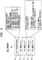
- each test program 23 is comprised of a header portion 24 and at least one, and up to two hundred fifty-five separate modules 25 (only the modules #0, #1, #4 and #16 being shown by way of illustration).
- test programs for each of the BSMs could be collectively stored by a magnetic disk 26.
- the test programs 23 are stored by the disk 26, then the need for the EPROMS 221 - 22 n would be obviated.
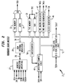
- the BSM 201 includes a Generic Processor Interface (GPI) 27, in the form of a microprocessor or the like, that is operative to control the testing of the board 121 in accordance with the test program 23 of FIG. 1 specific to the board.
- the GPI 27 has an eight bit data bus (D0-D7), a single bit address line (RA) and control bus that includes a read/write control signal line (R/W*), a data valid signal line (DAV*), and a chip-enable signal line (CE*).
- the clocking of the GPI 27 is controlled by a clock signal TCKIN.
- the GPI 27 is coupled, via a bidirectional bus 28, to an internal register bank 29 that contains a plurality of registers, typically eighteen in number.
- Table I provides an indication of the identity and function of the registers contained in the register bank 29.
- the register bank 29 is coupled via a bidirectional bus 30 to a first memory bank (32) and to an automatic test pattern generator 34.
- the first memory bank 32 is designated as a Test Vector Output (TVO) memory because it stores a set of deterministic test vectors for testing the circuit board 121 of FIG. 1.
- the vectors in the TVO memory 32 are generated in advance of testing.
- the Automatic Test Pattern Generator (ATPG) 34 typically takes the form of a Linear Feedback Shift Register that generates a separate one of four different patterns of test vectors in accordance with information stored in the Test Vector Manipulation register within the BSM internal register bank 29.
- the TVO memory 32 and the APTG 34 are coupled to a first and a second input, respectively, of a multiplexer 36 that passes the signal at a selected one of its first and second inputs to its output, designated as the Test Data Output (TDO) of the BSM 201.
- TDO Test Data Output
- the TDO output of the BSM 201 is coupled to a test data input of the chain of Boundary-Scan cells 141 - 14 p of FIG. 1.
- the register bank 29 is also coupled by the bus 30 to a second memory bank 38, designated as the Test Vector Input (TVI) memory bank.
- the TVI memory bank 38 stores responses generated by the chain of Boundary-Scan cells 141 - 14 p of FIG. 1, in response to test vectors supplied thereto, via the multiplexer 36.
- the responses generated by the circuit board 121 of FIG. 1 are also compacted by a Linear Feedback Shift Register 40.
- the register 40 is designated as the Signature Analysis Register (SAR) because it stores a signature (i.e., a compacted set of responses) indicative of the operation of the circuit board 121 of FIG. 1.
- SAR Signature Analysis Register
- the BSM 20 1 of FIG. 2 includes a pair of Test Mode Select (TMS) signal generators 42 and 44, each coupled to the bus 30.
- TMS generators 42 and 44 each generate a separate one of a pair of TMS signals, TMSO and TMS1, respectively, which is capable of controlling a separate one of a pair of chains of Boundary-Scan cells in accordance with the Boundary-Scan test technique described in the ANSI/IEEE Standard 1149.1 Test Access Port and Boundary-Scan Architecture , incorporated by reference herein.
- TMS Test Mode Select
- a clock generator 46 coupled to the bus 30, for generating a clock signal TCK supplied to the components (not shown) on the circuit board 121 of FIG. 1 during intervals of Boundary-Scan testing.
- the clock generator 46 generates the TCK signal by a programmable value, ranging from one to one hundred twenty- eight.
- the reason why the clock generator 46 effectively slows down the TCK signal is that often, there may be one or more slow components 15, each associated with a separate one of the Boundary-Scan cells 141 - 14 p within the Boundary-Scan chain. As a consequence, the clock speed must be slowed to the required clock speed of the slowest component 15.
- the BSM 201 also includes an interrupt/sample logic circuit 48 coupled to the bus 30.
- the interrupt/sample logic typically comprises a register and associated random logic that is clocked by a timer/counter 50.
- the function of the interrupt/sample logic 48 is to facilitate sampling of information generated by the chain of Boundary-Scan cells during testing. To sample the information, the circuit 48 is triggered by a sample signal SP*. In response to the sample signal SP*, the interrupt/sample logic 48 generates an interrupt INT* to signify that it is ready to provide the sampled data which is read via bus 30.
- the BSM 201 further includes a System-Level Boundary-Scan (B-S) Ring Configuration Logic circuit 52 of the type described in U.S. patent 5,029,166 (herein incorporated by reference) for allowing the BSM to operate in both a uniring or multi-ring mode.
- B-S System-Level Boundary-Scan
- the BSM 201 When operating in the uni-ring mode, the BSM 201 functions independently of the other BSMs and serves to test only the chain of Boundary-Scan cells 141 - 14 p on the circuit board 121.
- the BSM 201 cooperates with one or more other BSMs to test the individual chains of Boundary-Scan cells 141 - 14 p .
- the interpreter 18 comprises a set of data registers 54-60, a set of control registers 62-68, and a set of status registers 74.
- the data register 54 is designated as a Base Address Register as it stores a beginning (base) address of the test program 23 in each of the EPROMs 221 - 22 n . From this address, the location any of the modules 25 of the test program stored in a corresponding EPROM can be established.
- the register 56 is designated as the Program Counter, as it maintains the location currently being accessed within a particular one of the EPROMS 221 - 22 n .
- the register 58 is designated as the Bit Counter because this register accumulates the number of bits read back from a particular one of the BSMs 201 - 20 n in response to a specific read instruction (RDB) which is executed to read the registers in the internal register bank 29 of FIG. 2.
- RDB read instruction
- the Bit Counter 58 tracks the identification of a bit that has been found mismatched within the test program 23 in order to provide the highest level of diagnostic resolution supported by the BVM 17. Every time a bit is found to be mismatched, its location within the test program stored in the EPROM, as identified by the counter 58, is logged.
- the data register 60 is designated as the Mismatch Counter as it counts the number of mismatches. When the number of mismatches reaches a prescribed value, as counted by the Mismatch counter 60, error logging (i.e. counting of mismatches) is terminated.
- the control register 62 is designated as the Level of Error Log register, as it stores a value (typically 2 bits-wide) indicative of the level of error logging requested by the system test and diagnosis host 16.
- the control register 64 is designated as the Maximum Size Of Error Log register as it stores a value that sets a size limit on the error log.
- Control register 66 is designated as the Flow Control Type Register as it contains a value specifying the type of flow control to be followed in executing the test program 20. Depending on the value stored in the register 66, successive modules 25 of the test program 23 are executed under the control of the system test and diagnosis host 16, or a default flow control embedded in the test program is followed.
- Control register 68 is designated as a Checksum/Cyclic Redundancy Check (CRC) register, The register 68 stores a value contained in the test program 23 which dictates whether a checksum or a CRC is executed.
- CRC Checksum/Cyclic Redundancy Check
- the status register 70 is designated as the Error Log Overflow Flag as it functions to indicate when the error log has overflowed and error logging should terminate.
- the status register 72 is designated as the Test Module Data/Chk Fail Flags, as the register contains two values, each serving as a flag to indicate whether the current module 25 (see FIG. 3) of the test program 23 of FIGs. 1 and 3 has failed (that is, any bit has been found mismatched) or whether its checksum/CRC value failed to match. These two flags can be used to evaluate the pass/fail status of the current test module 25.
- the last status register 74 is designated as the test Program Data/Chk Fail Flags, as the register contains two values that record whether the current test program 23 has failed while executing or whether its checksum/CRC has failed.
- the two values in the register 76 can be used to evaluate the pass/fail nature of the entire program.
- the header 24 contains the preamble of the test program.
- a begin program header operation code which signifies the beginning of the test program
- the header 24 also contains the following information: (1) the circuit board identity, (2) the particular version of the board, (3) the contents of the test program (the number and locations of the test modules), and (4) whether a checksum or CRC is being used to verify the test program's integrity.
- an end program header code At the end of the test program is an end program header code to signify that the program header contains no further instructions.
- the test program 23 also contains a plurality of test modules 25, each containing a test that is to be applied to the circuit board.
- the test modules 25 may include a BSM self-test, a Boundary-Scan integrity test, an interconnect test, Built-In Self-Test execution (if any of the components 15 are so equipped), as well as a cluster test.
- each test module 25 starts with a begin test module operation code, indicating that the test module is to begin. Following the begin test module command is the body of the test module which contains instructions that program the BSM to execute a particular test, as well as test stimuli, and expected test signatures.
- the end of the test module is indicated by way of an End Test Module operation code which contains branching information as well as a checksum or CRC.
- the BVM 17 of FIG. 1 operates to accomplish testing of the circuit boards 121 - 12 n in the following manner.
- an initiate test command is sent from the system test and diagnosis host 16 to the BVM 17 to initiate testing.
- the system diagnostic host 16 also passes various parameters to the BVM 17, including the location of the test program, the desired degree of diagnostic resolution, type of flow control etc.
- the information passed by the system test and diagnosis host 16 is devoid of the particular details concerning each of the individual circuit boards 201 - 20 n .
- the BVM 17 causes each corresponding one of the BSMs 201 - 20 n to execute its entire test program 23 of FIGS. 1 and 3, including all of the test modules 25 of FIG. 3.
- While the system test and diagnosis host 16 of FIG. 1 does not directly determine which of the test modules 25 of FIG. 3 are executed under default flow control, the host nevertheless requires access to the test program header 24 of FIG. 3 prior to test program execution in order to determine an upper bound for test program duration. The reason for obtaining this information is to enable the test and diagnosis host 16 to protect against the possibility that the BVM 17 may wait indefinitely for a specific event that may never occur.
- the test and diagnosis host 16 would invoke the BVM 17 through the interpreter 18 of FIG. 1 to gain access to the test program header 24 of FIG. 3.
- the interpreter 18 would pass the program header 24 and then terminate. Thereafter, the test and diagnosis host would invoke the BVM 17 through the interpreter 18 to enable the interpreter to operate under default flow control.
- the starting point for the interpreter 18 will also be the header 24 of the test program since the information contained in the header is needed for default flow control.
- the interpreter 18 When the interpreter 18 is invoked, the first operation code encountered in the test program must be the Begin Program Header code in the program header 24 of FIG. 3, signifying the start of the test program header. If this operation code is not encountered, then execution of the test program must be terminated.
- the Begin Program Header operation code is encountered as the first instruction of the test program header 24, as will normally be the case, then the interpreter 18 stores certain information contained therein in order to set the appropriate parameters for the various registers 54-74.
- the checksum/CRC for the program header is computed. If the check fails, execution of the test program header 24 is terminated.
- the first test module 25 following the test program header is executed, one instruction at a time by the corresponding BSM.
- the nature of the instructions will depend on the type of test being executed. For example, one or more read operations may be executed after which a comparison occurs between each byte read and its expected value after applying a mask. Failure of a match between the byte just read and the masked expected byte causes the test module data fail flag contained in register 72 of FIG. 1 to be set. Also, upon the execution of each read operation, the bit counter (register 58) is incremented. Further failure information, as requested by the test and diagnosis host is logged.
- the checksum/CRC is computed. At the end of execution of the test module 25, the checksum/CRC is tested. If the checksum/CRC fails, the test module check fail flag contained in register 72 is set. Should either of the flags contained in register be set, then the test program fail flag contained in register 74 will be set.
- Operation under the test and diagnosis host 16 is generally simpler than operation under default flow control.
- the interpreter 18 of the BVM 17, through the corresponding BSM looks for the Begin Program Header in the test program header 24 and thereafter computes the checksum/CRC before exiting the test program header upon an End Program Header operation code. If the first- operation code is a Begin Test Module operation code, then the first test module 25 is executed by the BSM, whereupon the test program module is then exited upon the End Test Module operation code. Error logging and computation of the checksum/CRC are also performed. Under operation of the system test and diagnosis host 16, the interpreter 18 executes only a single test module 25 (or the program header 24) at one time and thereafter awaits instructions from the system test and diagnosis host as to which test module is to executed next.
- test system (10) for testing at least one, and a preferably a plurality of circuit boards 121 - 12 n , each containing at least one chain of Boundary-Scan cells 141 - 14 p .
Abstract
Description
- This invention relates to a method and an apparatus for testing one or more circuit boards in a system wherein each board contains a plurality of Boundary-Scan-testable electronic components coupled to each other.
- Traditionally, circuit boards have been tested via a bed-of-nails test fixture to detect faults, such as a failed connection between a node (i.e., a pin) of one component (e.g., an integrated circuit) on the board and a node of another component on the same board. As the density of components on a circuit board has increased, testing via the traditional bed-of-nails fixture has become increasingly more difficult to perform because of a reduced access to the nodes of the components on the board. For this reason, many circuit boards are now being designed with a Boundary-Scan test architecture of the type set forth in the ANSI/IEEE Standard 1149.1, Test Access Port and Boundary-Scan Architecture, incorporated by reference herein.
- In accordance with the ANSI/IEEE Boundary-Scan architecture, selected components on the board are each provided with one or more Boundary-Scan cells, each comprising a single-bit register. Each Boundary-Scan cell is coupled to a node of a component, such as an input, output, input/output or control node. The Boundary-Scan cells are serially coupled in a single chain, usually referred to as a Boundary-Scan chain. To accomplish Boundary-Scan testing of a board, a string of bits is shifted through the chain of Boundary-Scan cells so that each bit is latched in a separate cell in the chain. As the bits are shifted through the chain of Boundary-Scan cells, each cell coupled to an output node of a component is "updated," i.e., the bit shifted into the cell appears at the corresponding output node coupled to it. In turn, the bit appearing at an output node will be "captured" by a Boundary-Scan cell associated with an input node of a component driven by this output node. To check whether the connections between the Boundary-Scan-testable components are fault-free, the bits in the chain of Boundary-Scan cells are shifted out and compared to a bit string obtained under fault-free conditions.
- Boundary-Scan testing in the manner described above is controlled by way of a Boundary-Scan Master (BSM) on each circuit board. The BSM is comprised of a logic block that receives test information from a test and diagnosis host (i.e., a processor). In response to a test command from a host test and diagnosis processor specific to the type of circuit board to be tested, the BSM on that board accomplishes Boundary-Scan testing of the components that are coupled in the Boundary-Scan chain. In addition, the BSM may also initiate Built-In Self-Testing (BIST) of those components on the circuit board having such a capability. Further, the BSM may also be provided with the capability of compressing responses generated by the Boundary-Scan-testable components upon the completion of testing.
- In theory, each BSM affords its associated circuit board an ability to accomplish nearly complete self-testing that can be exploited during testing of a system containing multiple boards. Yet there are practical limitations that have heretofore adversely affected the ability to accomplish optimal Boundary-Scan testing on a system level. For example, different systems tend to utilize different types of test and diagnosis processors, thus giving rise to different processor architectures for which account must be taken. Different protocols may also exist which adds to the issue of variability.
- Further, tests performed at the system level are primarily functional tests and, as such, are generally independent of changes or revisions to the boards themselves. By contrast, Boundary-Scan and Built-In Self-Test techniques generally accomplish structural testing that may be affected by changes in the components on the board and/or the interconnections between them. Heretofore, it has been necessary to modify the system test and diagnosis software to take account of such changes, even if they do not affect the system functionality.
- Thus, there is a need for a Boundary-Scan-based test and diagnosis technique that is simple and affords early fault detection with a high degree of accuracy.
- Briefly, in accordance with a preferred embodiment of the invention, there is provided a system for testing at least one circuit board containing a plurality of Boundary-Scan-testable components connected to each other, as recited in
claim 1. -
- FIGURE 1 is a block schematic diagram of a test system in accordance with a preferred embodiment of the invention, for testing at least one circuit board;
- FIGURE 2 is a block schematic diagram of a Boundary-Scan master comprising part of the test system of FIG. 1; and
- FIGURE 3 is a table listing a portion of a test program for testing one of the circuit boards of FIG. 1.
- FIGURE 1 illustrates a
test system 10, in accordance with a preferred embodiment of the invention, for testing a plurality ofcircuit boards circuit boards Scan cells electronic component 15, such as an integrated circuit or the like. Each Boundary-Scan cell is responsive to the state of the signal present at thecomponent 15 node associated with that cell to facilitate testing of the interconnections between the components in accordance with the Boundary-Scan test technique described at the outset. - The
test system 10 includes a system test and diagnosis host (i.e., processor) 16 for initiating testing of the circuit boards 12₁ - 12 n to functionally test the system collectively formed by the boards. The test anddiagnosis host 16 may take the form of a processor that is dedicated to initiating and managing testing of the circuit boards 12₁ - 12 n . Alternatively, the test anddiagnosis host 16 may take the form of a processor that performs a variety of functions, only one of which involves initiation and management of the testing of the circuit boards 12₁ - 12 n . Regardless of whether the system test anddiagnosis host 16 manages testing of the circuit boards on an exclusive basis or on a shared basis with other tasks, the test and diagnosis host, in accordance with the invention, only manages the testing and diagnosis of the circuit boards 12₁ - 12 n on a system level. In other words, the test anddiagnosis host 16 does not control the actual testing of each individual circuit board and, thus, is not concerned with the specific details of each board. - Actual testing of the circuit boards 12₁ - 12 n is carried out by a Boundary-Scan Master Virtual Machine (BVM) 17 that includes an
interpreter 18 and a plurality of Boundary-Scan Masters (BSMs) 20₁,20₂...20 n , all coupled to the BVM interpreter via abus 21. Each of theBSMs - Associated with each of the BSMs 20₁ - 20 n is a separate one of a plurality of Electrically Programmable Read-Only Memories (EPROMs) 22₁,22₂...22 n . Each EPROM 22 i stores a
separate test program 23 unique to its corresponding BSM. As best seen in FIG. 3, which will be described in greater detail below, eachtest program 23 is comprised of aheader portion 24 and at least one, and up to two hundred fifty-five separate modules 25 (only themodules # 0, #1, #4 and #16 being shown by way of illustration). Referring to FIG. 1, instead of storing thetest program 23 for each of the BSMs 20₁ - 20 n within the corresponding one of the EPROMS 22₁ - 22 n , the test programs for each of the BSMs could be collectively stored by amagnetic disk 26. In the event that thetest programs 23 are stored by thedisk 26, then the need for the EPROMS 22₁ - 22 n would be obviated. - The BSMs 20₁ - 20 n are identical to each other and therefore only the
BSM 20₁ will be described in detail. Referring to FIG. 2, theBSM 20₁ includes a Generic Processor Interface (GPI) 27, in the form of a microprocessor or the like, that is operative to control the testing of theboard 12₁ in accordance with thetest program 23 of FIG. 1 specific to the board. TheGPI 27 has an eight bit data bus (D0-D7), a single bit address line (RA) and control bus that includes a read/write control signal line (R/W*), a data valid signal line (DAV*), and a chip-enable signal line (CE*). The clocking of theGPI 27 is controlled by a clock signal TCKIN. - The
GPI 27 is coupled, via abidirectional bus 28, to aninternal register bank 29 that contains a plurality of registers, typically eighteen in number. Table I provides an indication of the identity and function of the registers contained in theregister bank 29.

- The
register bank 29 is coupled via abidirectional bus 30 to a first memory bank (32) and to an automatictest pattern generator 34. Thefirst memory bank 32 is designated as a Test Vector Output (TVO) memory because it stores a set of deterministic test vectors for testing thecircuit board 12₁ of FIG. 1. The vectors in theTVO memory 32 are generated in advance of testing. The Automatic Test Pattern Generator (ATPG) 34 typically takes the form of a Linear Feedback Shift Register that generates a separate one of four different patterns of test vectors in accordance with information stored in the Test Vector Manipulation register within the BSMinternal register bank 29. TheTVO memory 32 and theAPTG 34 are coupled to a first and a second input, respectively, of amultiplexer 36 that passes the signal at a selected one of its first and second inputs to its output, designated as the Test Data Output (TDO) of theBSM 20₁. The TDO output of theBSM 20₁ is coupled to a test data input of the chain of Boundary-Scan cells 14₁ - 14 p of FIG. 1. - The
register bank 29 is also coupled by thebus 30 to asecond memory bank 38, designated as the Test Vector Input (TVI) memory bank. TheTVI memory bank 38 stores responses generated by the chain of Boundary-Scan cells 14₁ - 14 p of FIG. 1, in response to test vectors supplied thereto, via themultiplexer 36. The responses generated by thecircuit board 12₁ of FIG. 1 are also compacted by a LinearFeedback Shift Register 40. Theregister 40 is designated as the Signature Analysis Register (SAR) because it stores a signature (i.e., a compacted set of responses) indicative of the operation of thecircuit board 12₁ of FIG. 1. - The BSM 20 ₁ of FIG. 2 includes a pair of Test Mode Select (TMS)
signal generators bus 30. TheTMS generators TMS generators - Also associated with the
BSM 20₁ is aclock generator 46, coupled to thebus 30, for generating a clock signal TCK supplied to the components (not shown) on thecircuit board 12₁ of FIG. 1 during intervals of Boundary-Scan testing. Theclock generator 46 generates the TCK signal by a programmable value, ranging from one to one hundred twenty- eight. The reason why theclock generator 46 effectively slows down the TCK signal is that often, there may be one or moreslow components 15, each associated with a separate one of the Boundary-Scan cells 14₁ - 14 p within the Boundary-Scan chain. As a consequence, the clock speed must be slowed to the required clock speed of theslowest component 15. - The
BSM 20₁ also includes an interrupt/sample logic circuit 48 coupled to thebus 30. The interrupt/sample logic typically comprises a register and associated random logic that is clocked by a timer/counter 50. The function of the interrupt/sample logic 48 is to facilitate sampling of information generated by the chain of Boundary-Scan cells during testing. To sample the information, thecircuit 48 is triggered by a sample signal SP*. In response to the sample signal SP*, the interrupt/sample logic 48 generates an interrupt INT* to signify that it is ready to provide the sampled data which is read viabus 30. - The
BSM 20₁ further includes a System-Level Boundary-Scan (B-S) RingConfiguration Logic circuit 52 of the type described in U.S. patent 5,029,166 (herein incorporated by reference) for allowing the BSM to operate in both a uniring or multi-ring mode. When operating in the uni-ring mode, theBSM 20₁ functions independently of the other BSMs and serves to test only the chain of Boundary-Scan cells 14₁ - 14 p on thecircuit board 12₁. When operating in the multi-ring mode, theBSM 20₁ cooperates with one or more other BSMs to test the individual chains of Boundary-Scan cells 14₁ - 14 p . - As discussed, control of the individual BSMs 20₁ - 20 n is accomplished by the
BVM interpreter 18 of FIG. 1. Referring to FIG. 1, theinterpreter 18 comprises a set of data registers 54-60, a set of control registers 62-68, and a set of status registers 74. The data register 54 is designated as a Base Address Register as it stores a beginning (base) address of thetest program 23 in each of the EPROMs 22₁ - 22 n . From this address, the location any of themodules 25 of the test program stored in a corresponding EPROM can be established. Theregister 56 is designated as the Program Counter, as it maintains the location currently being accessed within a particular one of the EPROMS 22₁ - 22 n . Theregister 58 is designated as the Bit Counter because this register accumulates the number of bits read back from a particular one of the BSMs 20₁ - 20 n in response to a specific read instruction (RDB) which is executed to read the registers in theinternal register bank 29 of FIG. 2. TheBit Counter 58 tracks the identification of a bit that has been found mismatched within thetest program 23 in order to provide the highest level of diagnostic resolution supported by theBVM 17. Every time a bit is found to be mismatched, its location within the test program stored in the EPROM, as identified by thecounter 58, is logged. - The data register 60 is designated as the Mismatch Counter as it counts the number of mismatches. When the number of mismatches reaches a prescribed value, as counted by the
Mismatch counter 60, error logging (i.e. counting of mismatches) is terminated. - The control register 62 is designated as the Level of Error Log register, as it stores a value (typically 2 bits-wide) indicative of the level of error logging requested by the system test and
diagnosis host 16. The control register 64 is designated as the Maximum Size Of Error Log register as it stores a value that sets a size limit on the error log.Control register 66 is designated as the Flow Control Type Register as it contains a value specifying the type of flow control to be followed in executing the test program 20. Depending on the value stored in theregister 66,successive modules 25 of thetest program 23 are executed under the control of the system test anddiagnosis host 16, or a default flow control embedded in the test program is followed.Control register 68 is designated as a Checksum/Cyclic Redundancy Check (CRC) register, Theregister 68 stores a value contained in thetest program 23 which dictates whether a checksum or a CRC is executed. - The
status register 70 is designated as the Error Log Overflow Flag as it functions to indicate when the error log has overflowed and error logging should terminate. Thestatus register 72 is designated as the Test Module Data/Chk Fail Flags, as the register contains two values, each serving as a flag to indicate whether the current module 25 (see FIG. 3) of thetest program 23 of FIGs. 1 and 3 has failed (that is, any bit has been found mismatched) or whether its checksum/CRC value failed to match. These two flags can be used to evaluate the pass/fail status of thecurrent test module 25. Thelast status register 74 is designated as the test Program Data/Chk Fail Flags, as the register contains two values that record whether thecurrent test program 23 has failed while executing or whether its checksum/CRC has failed. The two values in the register 76 can be used to evaluate the pass/fail nature of the entire program. - Referring to FIG. 3, there is the detail of the
test program 23, which, as discussed, includes theheader 24 and a plurality ofseparate modules 25. Theheader 24 contains the preamble of the test program. In addition to a begin program header operation code, which signifies the beginning of the test program, theheader 24 also contains the following information: (1) the circuit board identity, (2) the particular version of the board, (3) the contents of the test program (the number and locations of the test modules), and (4) whether a checksum or CRC is being used to verify the test program's integrity. At the end of the test program is an end program header code to signify that the program header contains no further instructions. - The
test program 23 also contains a plurality oftest modules 25, each containing a test that is to be applied to the circuit board. Thetest modules 25 may include a BSM self-test, a Boundary-Scan integrity test, an interconnect test, Built-In Self-Test execution (if any of thecomponents 15 are so equipped), as well as a cluster test. As seen in FIG. 3, eachtest module 25 starts with a begin test module operation code, indicating that the test module is to begin. Following the begin test module command is the body of the test module which contains instructions that program the BSM to execute a particular test, as well as test stimuli, and expected test signatures. The end of the test module is indicated by way of an End Test Module operation code which contains branching information as well as a checksum or CRC. - The
BVM 17 of FIG. 1 operates to accomplish testing of the circuit boards 12₁ - 12 n in the following manner. First, an initiate test command is sent from the system test anddiagnosis host 16 to theBVM 17 to initiate testing. In addition to the initiate testing command, the systemdiagnostic host 16 also passes various parameters to theBVM 17, including the location of the test program, the desired degree of diagnostic resolution, type of flow control etc. As should be appreciated, the information passed by the system test anddiagnosis host 16 is devoid of the particular details concerning each of the individual circuit boards 20₁ - 20 n . - As alluded to previously, there are two modes of operation for the BVM 17: (1) default flow control, and (2) operation under the control of the system test and
diagnosis host 16. Operation under default flow control occurs in the absence of a command by the test and diagnosis host to execute specific test modules. Thus, under default flow control operation, theBVM 17 causes each corresponding one of the BSMs 20₁ - 20 n to execute itsentire test program 23 of FIGS. 1 and 3, including all of thetest modules 25 of FIG. 3. - While the system test and
diagnosis host 16 of FIG. 1 does not directly determine which of thetest modules 25 of FIG. 3 are executed under default flow control, the host nevertheless requires access to thetest program header 24 of FIG. 3 prior to test program execution in order to determine an upper bound for test program duration. The reason for obtaining this information is to enable the test anddiagnosis host 16 to protect against the possibility that theBVM 17 may wait indefinitely for a specific event that may never occur. Typically, the test anddiagnosis host 16 would invoke theBVM 17 through theinterpreter 18 of FIG. 1 to gain access to thetest program header 24 of FIG. 3. Theinterpreter 18 would pass theprogram header 24 and then terminate. Thereafter, the test and diagnosis host would invoke theBVM 17 through theinterpreter 18 to enable the interpreter to operate under default flow control. The starting point for theinterpreter 18 will also be theheader 24 of the test program since the information contained in the header is needed for default flow control. - When the
interpreter 18 is invoked, the first operation code encountered in the test program must be the Begin Program Header code in theprogram header 24 of FIG. 3, signifying the start of the test program header. If this operation code is not encountered, then execution of the test program must be terminated. When the Begin Program Header operation code is encountered as the first instruction of thetest program header 24, as will normally be the case, then theinterpreter 18 stores certain information contained therein in order to set the appropriate parameters for the various registers 54-74. At the end of theprogram header 24 of FIG. 3, the checksum/CRC for the program header is computed. If the check fails, execution of thetest program header 24 is terminated. - Assuming that the checksum/CRC for the
test program header 24 passes, then thefirst test module 25 following the test program header is executed, one instruction at a time by the corresponding BSM. The nature of the instructions will depend on the type of test being executed. For example, one or more read operations may be executed after which a comparison occurs between each byte read and its expected value after applying a mask. Failure of a match between the byte just read and the masked expected byte causes the test module data fail flag contained inregister 72 of FIG. 1 to be set. Also, upon the execution of each read operation, the bit counter (register 58) is incremented. Further failure information, as requested by the test and diagnosis host is logged. - As each instruction of the
module 25 is executed, the checksum/CRC is computed. At the end of execution of thetest module 25, the checksum/CRC is tested. If the checksum/CRC fails, the test module check fail flag contained inregister 72 is set. Should either of the flags contained in register be set, then the test program fail flag contained inregister 74 will be set. - Operation under the test and
diagnosis host 16 is generally simpler than operation under default flow control. When operating under the test anddiagnosis host 16, theinterpreter 18 of theBVM 17, through the corresponding BSM, looks for the Begin Program Header in thetest program header 24 and thereafter computes the checksum/CRC before exiting the test program header upon an End Program Header operation code. If the first- operation code is a Begin Test Module operation code, then thefirst test module 25 is executed by the BSM, whereupon the test program module is then exited upon the End Test Module operation code. Error logging and computation of the checksum/CRC are also performed. Under operation of the system test anddiagnosis host 16, theinterpreter 18 executes only a single test module 25 (or the program header 24) at one time and thereafter awaits instructions from the system test and diagnosis host as to which test module is to executed next. - The foregoing describes a test system (10) for testing at least one, and a preferably a plurality of circuit boards 12₁ - 12 n , each containing at least one chain of Boundary-Scan cells 14₁ - 14 p .
- It is to be understood that the above-described embodiments are merely illustrative of the principles of the invention. Various modifications and changes may be made thereto by those skilled in the art which will embody the principles of the invention and fall within the spirit and scope thereof. For example. while the
interpreter 18 of FIG. 1 has been described in terms of a plurality of physical registers 54-74, it should be understood that the function of the interpreter could easily be performed by way of a software program, either running on a stand-alone machine, or running as part of the software executed by the system test anddiagnosis host 16.
Claims (5)
- A system for testing at least one circuit board containing a plurality of Boundary-Scan-testable electronic components coupled in a serial Boundary-Scan chain, CHARACTERIZED BY:
a test and diagnostic host processor (16) for generating an initiate test command to initiate Boundary-Scan testing of each board and for receiving test information indicative of its operation;
a Boundary-Scan Master Virtual Machine (BVM) (17) responsive to the initiate test command from the test and diagnostic host processor for communicating to each circuit board a test command to cause said circuit board to execute a test program specific thereto, thereby causing the board to undergo testing and to generate test results, the BVM interpreting the test results and communicating such results to the test and diagnostic host as test information indicative of the operation of the circuit board; and
a communications bus (21) coupling each circuit board to the BVM. - The system according to claim 1 wherein the BVM comprises:
a Boundary-Scan Master (BSM) (20), associated with and carried by each circuit board, the BSM executing the test program specific to the circuit board associated therewith to test the circuit board and to receive from the circuit board test information indicative of its operation;
a program storage memory (22) associated with each separate BSM for storing a test program specific to the circuit board which carries the BSM; and
a Boundary-Scan interpreter (18) for interpreting the initiate test command from the test and diagnosis host so as to cause each BSM to execute its corresponding test program to test its associated circuit board and for interpreting test information received from each BSM in order to provide the test and diagnosis host with test information indicative of the operation of the circuit boards. - The system according to claim 2 wherein the Boundary-Scan interpreter comprises:
a plurality of data registers (54-60) for storing information passed by the system test and diagnosis host to the BVM, including information indicative of the location of the test program and information related to errors in each circuit board detected during testing;
a plurality of control registers (62-68) for storing information to control the testing of each circuit board, including information related to the execution of the test program; and
a plurality of status registers (70-74) which record the status of errors occurring during testing. - The system according to claim 1 wherein each test program comprises:
a test program header (24) containing information indicative of the circuit board for which the program is to be executed and information indicative of which tests are to be performed upon the board; and
at least one test module (25) containing a test to be executed upon the circuit board. - A method for testing at least one circuit board (12) containing a plurality of Boundary-Scan-testable electronic components (14) coupled in a serial Boundary-Scan chain, comprising the steps of:
generating a high-level test command at a system test and diagnosis host (17) to initiate testing of the circuit board;
interpreting the test command from the system test and diagnosis host to provide a test instruction to each circuit board (12) to cause each circuit board to execute a test program specific thereto and to generate test results indicative of errors in the board; and
interpreting the test results from the circuit board (12) to establish test information indicative of the operation of the board which is transmitted to the system test and diagnosis host (17).
Applications Claiming Priority (2)
| Application Number | Priority Date | Filing Date | Title |
|---|---|---|---|
| US113460 | 1993-08-30 | ||
| US08/113,460 US5444716A (en) | 1993-08-30 | 1993-08-30 | Boundary-scan-based system and method for test and diagnosis |
Publications (2)
| Publication Number | Publication Date |
|---|---|
| EP0640920A1 true EP0640920A1 (en) | 1995-03-01 |
| EP0640920B1 EP0640920B1 (en) | 1999-02-10 |
Family
ID=22349570
Family Applications (1)
| Application Number | Title | Priority Date | Filing Date |
|---|---|---|---|
| EP94306040A Expired - Lifetime EP0640920B1 (en) | 1993-08-30 | 1994-08-17 | Boundary-scan-based system and method for test and diagnosis |
Country Status (8)
| Country | Link |
|---|---|
| US (1) | US5444716A (en) |
| EP (1) | EP0640920B1 (en) |
| JP (1) | JPH07181231A (en) |
| KR (1) | KR0138225B1 (en) |
| CA (1) | CA2127612C (en) |
| DE (1) | DE69416471T2 (en) |
| ES (1) | ES2130361T3 (en) |
| TW (1) | TW276300B (en) |
Cited By (2)
| Publication number | Priority date | Publication date | Assignee | Title |
|---|---|---|---|---|
| WO2004008319A2 (en) * | 2002-07-11 | 2004-01-22 | Advanced Micro Devices, Inc. | Method and apparatus for determining a processor state without interrupting processor operation |
| CN102621483A (en) * | 2012-03-27 | 2012-08-01 | 中国人民解放军国防科学技术大学 | Multi-link parallel boundary scanning testing device and method |
Families Citing this family (40)
| Publication number | Priority date | Publication date | Assignee | Title |
|---|---|---|---|---|
| US5774644A (en) * | 1993-12-17 | 1998-06-30 | International Business Machines Corporation | Method and apparatus for generating a pair of interoperating communications programs |
| US5537052A (en) * | 1994-06-17 | 1996-07-16 | Emc Corporation | System and method for executing on board diagnostics and maintaining an event history on a circuit board |
| WO1996042054A1 (en) * | 1995-06-09 | 1996-12-27 | Hal Computer Systems, Inc. | Method, system and apparatus for efficiently generating binary numbers for testing storage devices |
| US5706297A (en) * | 1995-08-24 | 1998-01-06 | Unisys Corporation | System for adapting maintenance operations to JTAG and non-JTAG modules |
| EP1632780A2 (en) * | 1995-12-27 | 2006-03-08 | Koken Co., Ltd. | Monitoring control apparatus |
| US5835503A (en) * | 1996-03-28 | 1998-11-10 | Cypress Semiconductor Corp. | Method and apparatus for serially programming a programmable logic device |
| US5768288A (en) * | 1996-03-28 | 1998-06-16 | Cypress Semiconductor Corp. | Method and apparatus for programming a programmable logic device having verify logic for comparing verify data read from a memory location with program data |
| US5815510A (en) * | 1996-03-28 | 1998-09-29 | Cypress Semiconductor Corp. | Serial programming of instruction codes in different numbers of clock cycles |
| US5805794A (en) * | 1996-03-28 | 1998-09-08 | Cypress Semiconductor Corp. | CPLD serial programming with extra read register |
| US5668947A (en) * | 1996-04-18 | 1997-09-16 | Allen-Bradley Company, Inc. | Microprocessor self-test apparatus and method |
| US5968196A (en) * | 1998-04-21 | 1999-10-19 | Atmel Corporation | Configuration control in a programmable logic device using non-volatile elements |
| US6378094B1 (en) * | 1999-04-01 | 2002-04-23 | Lucent Technologies Inc. | Method and system for testing cluster circuits in a boundary scan environment |
| US7493540B1 (en) | 1999-11-23 | 2009-02-17 | Jansuz Rajski | Continuous application and decompression of test patterns to a circuit-under-test |
| US6684358B1 (en) * | 1999-11-23 | 2004-01-27 | Janusz Rajski | Decompressor/PRPG for applying pseudo-random and deterministic test patterns |
| US6327687B1 (en) * | 1999-11-23 | 2001-12-04 | Janusz Rajski | Test pattern compression for an integrated circuit test environment |
| US6557129B1 (en) | 1999-11-23 | 2003-04-29 | Janusz Rajski | Method and apparatus for selectively compacting test responses |
| US6874109B1 (en) | 1999-11-23 | 2005-03-29 | Janusz Rajski | Phase shifter with reduced linear dependency |
| US9134370B2 (en) | 1999-11-23 | 2015-09-15 | Mentor Graphics Corporation | Continuous application and decompression of test patterns and selective compaction of test responses |
| US6353842B1 (en) * | 1999-11-23 | 2002-03-05 | Janusz Rajski | Method for synthesizing linear finite state machines |
| US9664739B2 (en) | 1999-11-23 | 2017-05-30 | Mentor Graphics Corporation | Continuous application and decompression of test patterns and selective compaction of test responses |
| US8533547B2 (en) * | 1999-11-23 | 2013-09-10 | Mentor Graphics Corporation | Continuous application and decompression of test patterns and selective compaction of test responses |
| EP1242885B1 (en) * | 1999-11-23 | 2009-10-07 | Mentor Graphics Corporation | Continuous application and decompression of test patterns to a circuit-under-test |
| AU2001227892A1 (en) * | 2000-01-14 | 2001-07-24 | Parthus Technologies Plc | An algorithmic test pattern generator, with built-in-self-test (bist) capabilities, for functional testing of a circuit |
| US6959257B1 (en) * | 2000-09-11 | 2005-10-25 | Cypress Semiconductor Corp. | Apparatus and method to test high speed devices with a low speed tester |
| US20020093356A1 (en) * | 2000-11-30 | 2002-07-18 | Williams Thomas W. | Intelligent test vector formatting to reduce test vector size and allow encryption thereof for integrated circuit testing |
| US6744256B2 (en) * | 2001-10-29 | 2004-06-01 | Agilent Technologies, Inc. | Boundary-scan testing of opto-electronic devices |
| US20050159925A1 (en) * | 2004-01-15 | 2005-07-21 | Elias Gedamu | Cache testing for a processor design |
| US20050172182A1 (en) * | 2004-01-15 | 2005-08-04 | Elias Gedamu | Optimal operational voltage identification for a processor design |
| US20050172178A1 (en) * | 2004-01-15 | 2005-08-04 | Elias Gedamu | Cache-testable processor identification |
| US7906982B1 (en) | 2006-02-28 | 2011-03-15 | Cypress Semiconductor Corporation | Interface apparatus and methods of testing integrated circuits using the same |
| US8615691B2 (en) * | 2006-10-13 | 2013-12-24 | Advantest (Singapore) Pte Ltd | Process for improving design-limited yield by localizing potential faults from production test data |
| US8453026B2 (en) * | 2006-10-13 | 2013-05-28 | Advantest (Singapore) Pte Ltd | Process for improving design limited yield by efficiently capturing and storing production test data for analysis using checksums, hash values, or digital fault signatures |
| US20080239082A1 (en) * | 2007-03-29 | 2008-10-02 | Analogix Semiconductor, Inc. | HDMI format video pattern and audio frequencies generator for field test and built-in self test |
| US9759772B2 (en) | 2011-10-28 | 2017-09-12 | Teradyne, Inc. | Programmable test instrument |
| US10776233B2 (en) | 2011-10-28 | 2020-09-15 | Teradyne, Inc. | Programmable test instrument |
| CN102520344B (en) * | 2011-12-16 | 2014-04-02 | 大唐微电子技术有限公司 | Boundary scanning module and boundary scanning system for smart card testing |
| US9595350B2 (en) * | 2012-11-05 | 2017-03-14 | Nxp Usa, Inc. | Hardware-based memory initialization |
| US10184980B2 (en) * | 2016-09-06 | 2019-01-22 | Texas Instruments Incorporated | Multiple input signature register analysis for digital circuitry |
| TWI736721B (en) * | 2017-12-13 | 2021-08-21 | 英業達股份有限公司 | Pin connection testing system for connector and method thereof |
| US10515039B2 (en) * | 2018-01-05 | 2019-12-24 | Molex, Llc | Vehicle USB hub system |
Citations (1)
| Publication number | Priority date | Publication date | Assignee | Title |
|---|---|---|---|---|
| EP0417905A2 (en) * | 1989-08-09 | 1991-03-20 | Texas Instruments Incorporated | System scan path architecture |
Family Cites Families (5)
| Publication number | Priority date | Publication date | Assignee | Title |
|---|---|---|---|---|
| US4872169A (en) * | 1987-03-06 | 1989-10-03 | Texas Instruments Incorporated | Hierarchical scan selection |
| US4872125A (en) * | 1987-06-26 | 1989-10-03 | Daisy Systems Corporation | Multiple processor accelerator for logic simulation |
| US5029166A (en) * | 1989-05-31 | 1991-07-02 | At&T Bell Laboratories | Method and apparatus for testing circuit boards |
| US5132635A (en) * | 1991-03-05 | 1992-07-21 | Ast Research, Inc. | Serial testing of removable circuit boards on a backplane bus |
| GB2260414A (en) * | 1991-10-10 | 1993-04-14 | Genrad Inc | Circuit tester with scanner path assignment |
-
1993
- 1993-08-30 US US08/113,460 patent/US5444716A/en not_active Expired - Fee Related
-
1994
- 1994-07-07 CA CA002127612A patent/CA2127612C/en not_active Expired - Fee Related
- 1994-08-10 TW TW083107398A patent/TW276300B/zh active
- 1994-08-17 DE DE69416471T patent/DE69416471T2/en not_active Expired - Fee Related
- 1994-08-17 ES ES94306040T patent/ES2130361T3/en not_active Expired - Lifetime
- 1994-08-17 EP EP94306040A patent/EP0640920B1/en not_active Expired - Lifetime
- 1994-08-29 KR KR1019940021970A patent/KR0138225B1/en not_active IP Right Cessation
- 1994-08-29 JP JP6226018A patent/JPH07181231A/en active Pending
Patent Citations (1)
| Publication number | Priority date | Publication date | Assignee | Title |
|---|---|---|---|---|
| EP0417905A2 (en) * | 1989-08-09 | 1991-03-20 | Texas Instruments Incorporated | System scan path architecture |
Non-Patent Citations (2)
| Title |
|---|
| J.-C. LIEN ET AL.: "Test program synthesis for modules and chips having boundary scan", JOURNAL OF ELECTRONIC TESTING, vol. 4, no. 2, May 1993 (1993-05-01), DORDRECHT NL, pages 159 - 180, XP000370003, DOI: doi:10.1007/BF00971645 * |
| N JARWALA ET AL.: "A structured approach to board-level BIST using the boundary-scan master", MICROPROCESSORS AND MICROSYSTEMS, vol. 17, no. 5, June 1993 (1993-06-01), LONDON GB, pages 289 - 297, XP000377918, DOI: doi:10.1016/0141-9331(93)90006-S * |
Cited By (4)
| Publication number | Priority date | Publication date | Assignee | Title |
|---|---|---|---|---|
| WO2004008319A2 (en) * | 2002-07-11 | 2004-01-22 | Advanced Micro Devices, Inc. | Method and apparatus for determining a processor state without interrupting processor operation |
| WO2004008319A3 (en) * | 2002-07-11 | 2004-05-21 | Advanced Micro Devices Inc | Method and apparatus for determining a processor state without interrupting processor operation |
| CN102621483A (en) * | 2012-03-27 | 2012-08-01 | 中国人民解放军国防科学技术大学 | Multi-link parallel boundary scanning testing device and method |
| CN102621483B (en) * | 2012-03-27 | 2014-04-16 | 中国人民解放军国防科学技术大学 | Multi-link parallel boundary scanning testing device and method |
Also Published As
| Publication number | Publication date |
|---|---|
| KR950006470A (en) | 1995-03-21 |
| TW276300B (en) | 1996-05-21 |
| EP0640920B1 (en) | 1999-02-10 |
| CA2127612C (en) | 1998-08-18 |
| US5444716A (en) | 1995-08-22 |
| JPH07181231A (en) | 1995-07-21 |
| DE69416471D1 (en) | 1999-03-25 |
| ES2130361T3 (en) | 1999-07-01 |
| KR0138225B1 (en) | 1998-06-15 |
| CA2127612A1 (en) | 1995-03-01 |
| DE69416471T2 (en) | 1999-08-05 |
Similar Documents
| Publication | Publication Date | Title |
|---|---|---|
| EP0640920A1 (en) | Boundary-scan-based system and method for test and diagnosis | |
| EP0370929A2 (en) | Kernel testing interface and method for automating diagnostics of microprocessor-based systems | |
| US5423050A (en) | Intermodule test across system bus utilizing serial test bus | |
| US5343478A (en) | Computer system configuration via test bus | |
| US5377198A (en) | JTAG instruction error detection | |
| US4868822A (en) | Memory emulation method and system for testing and troubleshooting microprocessor-based electronic systems | |
| US4709366A (en) | Computer assisted fault isolation in circuit board testing | |
| US5325368A (en) | JTAG component description via nonvolatile memory | |
| US4862067A (en) | Method and apparatus for in-circuit testing of electronic devices | |
| US4414669A (en) | Self-testing pipeline processors | |
| US5638383A (en) | Advanced integrated avionics testing system | |
| JPH07168767A (en) | Apparatus and method for built-in self-checking of smart memory | |
| US5325365A (en) | In a memory emulation test apparatus, a method of and system for fast functional testing of memories in microprocessor-based units | |
| US5068852A (en) | Hardware enhancements for improved performance of memory emulation method | |
| US4989207A (en) | Automatic verification of kernel circuitry based on analysis of memory accesses | |
| EP0120446A2 (en) | Digital equipment tester | |
| US7237168B2 (en) | Design for test of analog module systems | |
| US4958347A (en) | Apparatus, method and data structure for validation of kernel data bus | |
| Sedmark | Boundary-scan: beyond production test | |
| EP0296884A2 (en) | Method for in-circuit testing of electronic devices | |
| Chan | An improved technique for circuit board interconnect test | |
| US6256761B1 (en) | Integrated electronic module with hardware error infeed for checking purposes | |
| US7587649B2 (en) | Testing of reconfigurable logic and interconnect sources | |
| Pomeranz et al. | On the detection of reset faults; in synchronous sequential circuits | |
| JPS62122000A (en) | Memory element |
Legal Events
| Date | Code | Title | Description |
|---|---|---|---|
| PUAI | Public reference made under article 153(3) epc to a published international application that has entered the european phase |
Free format text: ORIGINAL CODE: 0009012 |
|
| AK | Designated contracting states |
Kind code of ref document: A1 Designated state(s): DE ES FR GB IT NL |
|
| 17P | Request for examination filed |
Effective date: 19950818 |
|
| 17Q | First examination report despatched |
Effective date: 19970520 |
|
| GRAG | Despatch of communication of intention to grant |
Free format text: ORIGINAL CODE: EPIDOS AGRA |
|
| GRAG | Despatch of communication of intention to grant |
Free format text: ORIGINAL CODE: EPIDOS AGRA |
|
| GRAG | Despatch of communication of intention to grant |
Free format text: ORIGINAL CODE: EPIDOS AGRA |
|
| GRAH | Despatch of communication of intention to grant a patent |
Free format text: ORIGINAL CODE: EPIDOS IGRA |
|
| GRAH | Despatch of communication of intention to grant a patent |
Free format text: ORIGINAL CODE: EPIDOS IGRA |
|
| GRAA | (expected) grant |
Free format text: ORIGINAL CODE: 0009210 |
|
| AK | Designated contracting states |
Kind code of ref document: B1 Designated state(s): DE ES FR GB IT NL |
|
| ITF | It: translation for a ep patent filed |
Owner name: JACOBACCI & PERANI S.P.A. |
|
| REF | Corresponds to: |
Ref document number: 69416471 Country of ref document: DE Date of ref document: 19990325 |
|
| ET | Fr: translation filed | ||
| REG | Reference to a national code |
Ref country code: ES Ref legal event code: FG2A Ref document number: 2130361 Country of ref document: ES Kind code of ref document: T3 |
|
| PLBE | No opposition filed within time limit |
Free format text: ORIGINAL CODE: 0009261 |
|
| STAA | Information on the status of an ep patent application or granted ep patent |
Free format text: STATUS: NO OPPOSITION FILED WITHIN TIME LIMIT |
|
| 26N | No opposition filed | ||
| PGFP | Annual fee paid to national office [announced via postgrant information from national office to epo] |
Ref country code: FR Payment date: 20010725 Year of fee payment: 8 |
|
| PGFP | Annual fee paid to national office [announced via postgrant information from national office to epo] |
Ref country code: GB Payment date: 20010726 Year of fee payment: 8 |
|
| PGFP | Annual fee paid to national office [announced via postgrant information from national office to epo] |
Ref country code: NL Payment date: 20010730 Year of fee payment: 8 |
|
| PGFP | Annual fee paid to national office [announced via postgrant information from national office to epo] |
Ref country code: ES Payment date: 20010803 Year of fee payment: 8 |
|
| PGFP | Annual fee paid to national office [announced via postgrant information from national office to epo] |
Ref country code: DE Payment date: 20010928 Year of fee payment: 8 |
|
| REG | Reference to a national code |
Ref country code: GB Ref legal event code: IF02 |
|
| PG25 | Lapsed in a contracting state [announced via postgrant information from national office to epo] |
Ref country code: GB Free format text: LAPSE BECAUSE OF NON-PAYMENT OF DUE FEES Effective date: 20020817 |
|
| PG25 | Lapsed in a contracting state [announced via postgrant information from national office to epo] |
Ref country code: ES Free format text: LAPSE BECAUSE OF NON-PAYMENT OF DUE FEES Effective date: 20020818 |
|
| PG25 | Lapsed in a contracting state [announced via postgrant information from national office to epo] |
Ref country code: NL Free format text: LAPSE BECAUSE OF NON-PAYMENT OF DUE FEES Effective date: 20030301 Ref country code: DE Free format text: LAPSE BECAUSE OF NON-PAYMENT OF DUE FEES Effective date: 20030301 |
|
| GBPC | Gb: european patent ceased through non-payment of renewal fee |
Effective date: 20020817 |
|
| PG25 | Lapsed in a contracting state [announced via postgrant information from national office to epo] |
Ref country code: FR Free format text: LAPSE BECAUSE OF NON-PAYMENT OF DUE FEES Effective date: 20030430 |
|
| NLV4 | Nl: lapsed or anulled due to non-payment of the annual fee |
Effective date: 20030301 |
|
| REG | Reference to a national code |
Ref country code: FR Ref legal event code: ST |
|
| REG | Reference to a national code |
Ref country code: ES Ref legal event code: FD2A Effective date: 20030912 |
|
| PG25 | Lapsed in a contracting state [announced via postgrant information from national office to epo] |
Ref country code: IT Free format text: LAPSE BECAUSE OF NON-PAYMENT OF DUE FEES Effective date: 20050817 |