EP0640887B1 - Nettoyage électrostatique avec tension continue pour les filaments non abrasés d'électrode - Google Patents
Nettoyage électrostatique avec tension continue pour les filaments non abrasés d'électrode Download PDFInfo
- Publication number
- EP0640887B1 EP0640887B1 EP94305840A EP94305840A EP0640887B1 EP 0640887 B1 EP0640887 B1 EP 0640887B1 EP 94305840 A EP94305840 A EP 94305840A EP 94305840 A EP94305840 A EP 94305840A EP 0640887 B1 EP0640887 B1 EP 0640887B1
- Authority
- EP
- European Patent Office
- Prior art keywords
- electrode structure
- wire electrode
- voltage
- toner
- transport means
- Prior art date
- Legal status (The legal status is an assumption and is not a legal conclusion. Google has not performed a legal analysis and makes no representation as to the accuracy of the status listed.)
- Expired - Lifetime
Links
- 238000011161 development Methods 0.000 title claims description 59
- 238000004140 cleaning Methods 0.000 title claims description 23
- 239000002245 particle Substances 0.000 claims description 38
- 238000000034 method Methods 0.000 claims description 19
- 230000001846 repelling effect Effects 0.000 claims 1
- 230000018109 developmental process Effects 0.000 description 56
- 230000005291 magnetic effect Effects 0.000 description 36
- 239000000463 material Substances 0.000 description 32
- 230000032258 transport Effects 0.000 description 13
- 230000005686 electrostatic field Effects 0.000 description 12
- 239000000356 contaminant Substances 0.000 description 10
- 238000007639 printing Methods 0.000 description 9
- 239000008187 granular material Substances 0.000 description 7
- 239000000843 powder Substances 0.000 description 7
- 230000000694 effects Effects 0.000 description 5
- 230000005684 electric field Effects 0.000 description 4
- 230000008569 process Effects 0.000 description 4
- 230000008901 benefit Effects 0.000 description 3
- 238000011109 contamination Methods 0.000 description 3
- 230000008021 deposition Effects 0.000 description 3
- 230000000670 limiting effect Effects 0.000 description 3
- 230000033001 locomotion Effects 0.000 description 3
- 238000009825 accumulation Methods 0.000 description 2
- XAGFODPZIPBFFR-UHFFFAOYSA-N aluminium Chemical compound [Al] XAGFODPZIPBFFR-UHFFFAOYSA-N 0.000 description 2
- 229910052782 aluminium Inorganic materials 0.000 description 2
- 239000003990 capacitor Substances 0.000 description 2
- 239000006229 carbon black Substances 0.000 description 2
- 239000004020 conductor Substances 0.000 description 2
- 230000008878 coupling Effects 0.000 description 2
- 238000010168 coupling process Methods 0.000 description 2
- 238000005859 coupling reaction Methods 0.000 description 2
- 238000013016 damping Methods 0.000 description 2
- 230000009977 dual effect Effects 0.000 description 2
- 238000003384 imaging method Methods 0.000 description 2
- 230000009191 jumping Effects 0.000 description 2
- 230000002829 reductive effect Effects 0.000 description 2
- 239000012260 resinous material Substances 0.000 description 2
- 238000012360 testing method Methods 0.000 description 2
- OKTJSMMVPCPJKN-UHFFFAOYSA-N Carbon Chemical compound [C] OKTJSMMVPCPJKN-UHFFFAOYSA-N 0.000 description 1
- 229920000742 Cotton Polymers 0.000 description 1
- 238000013459 approach Methods 0.000 description 1
- 239000011324 bead Substances 0.000 description 1
- 230000015556 catabolic process Effects 0.000 description 1
- 230000008859 change Effects 0.000 description 1
- 239000011248 coating agent Substances 0.000 description 1
- 238000000576 coating method Methods 0.000 description 1
- 238000004040 coloring Methods 0.000 description 1
- 238000004891 communication Methods 0.000 description 1
- 230000003247 decreasing effect Effects 0.000 description 1
- 238000006731 degradation reaction Methods 0.000 description 1
- 230000001419 dependent effect Effects 0.000 description 1
- 238000013461 design Methods 0.000 description 1
- 238000010586 diagram Methods 0.000 description 1
- 230000005294 ferromagnetic effect Effects 0.000 description 1
- 239000000835 fiber Substances 0.000 description 1
- 229910002804 graphite Inorganic materials 0.000 description 1
- 239000010439 graphite Substances 0.000 description 1
- 230000006872 improvement Effects 0.000 description 1
- 230000003993 interaction Effects 0.000 description 1
- 230000002452 interceptive effect Effects 0.000 description 1
- 239000000203 mixture Substances 0.000 description 1
- 230000010355 oscillation Effects 0.000 description 1
- 229920000642 polymer Polymers 0.000 description 1
- 230000002441 reversible effect Effects 0.000 description 1
- 229910001220 stainless steel Inorganic materials 0.000 description 1
- 239000010935 stainless steel Substances 0.000 description 1
- 229920002554 vinyl polymer Polymers 0.000 description 1
Images

Classifications
-
- G—PHYSICS
- G03—PHOTOGRAPHY; CINEMATOGRAPHY; ANALOGOUS TECHNIQUES USING WAVES OTHER THAN OPTICAL WAVES; ELECTROGRAPHY; HOLOGRAPHY
- G03G—ELECTROGRAPHY; ELECTROPHOTOGRAPHY; MAGNETOGRAPHY
- G03G15/00—Apparatus for electrographic processes using a charge pattern
- G03G15/06—Apparatus for electrographic processes using a charge pattern for developing
- G03G15/08—Apparatus for electrographic processes using a charge pattern for developing using a solid developer, e.g. powder developer
- G03G15/0803—Apparatus for electrographic processes using a charge pattern for developing using a solid developer, e.g. powder developer in a powder cloud
-
- G—PHYSICS
- G03—PHOTOGRAPHY; CINEMATOGRAPHY; ANALOGOUS TECHNIQUES USING WAVES OTHER THAN OPTICAL WAVES; ELECTROGRAPHY; HOLOGRAPHY
- G03G—ELECTROGRAPHY; ELECTROPHOTOGRAPHY; MAGNETOGRAPHY
- G03G2215/00—Apparatus for electrophotographic processes
- G03G2215/06—Developing structures, details
- G03G2215/0634—Developing device
- G03G2215/0636—Specific type of dry developer device
- G03G2215/0643—Electrodes in developing area, e.g. wires, not belonging to the main donor part
Definitions
- This invention relates generally to the development of electrostatic latent images, and more particularly concerns a scavengeless development system in which an electrostatic bias is applied to the electrode wires.
- the process of electrophotographic printing includes charging a photoconductive member to a substantially uniform potential so as to sensitize the surface thereof.
- the charged portion of the photoconductive surface is exposed to a light image of an original document being reproduced.
- the latent image is developed by bringing a developer material into contact therewith.
- Two-component and single-component developer materials are commonly used.
- a typical two-component developer material comprises magnetic granules having toner particles adhering triboelectrically thereto.
- a single component developer material typically comprises toner particles. Toner particles are attracted to the latent image forming a toner powder image on the photoconductive surface.
- the toner powder image is subsequently transferred to a copy sheet.
- the toner powder image is heated to permanently fuse it to the copy sheet in image configuration.
- Single-component development systems use a donor roll for transporting charged toner to the development nip defined by the donor roll and photoconductive surface.
- the toner is developed on the latent image recorded on the photoconductive member by a combination of mechanical and/or electrical forces.
- Scavengeless development and jumping development are two types of single-component developments.
- a scavengeless development system uses a donor roll with a plurality of electrode wires closely spaced therefrom in the development zone. An AC voltage is applied to the wires forming a toner cloud in the development zone. The electrostatic field generated by the latent image attracts toner from the toner cloud to develop the latent image.
- a two-component development system In jumping development, an AC voltage is applied to the donor roll detaching toner from the donor roll and projecting the toner toward the photoconductive member so that the electrostatic fields generated by the latent image attract the toner to develop the latent image.
- Single-component development systems appear to offer advantages of low cost and design simplicity.
- Two-component development systems have been used extensively in many different types of printing machines.
- a two-component development system usually employs a magnetic brush developer roller for transporting carrier having toner adhering triboelectrically thereto. The electrostatic fields generated by the latent image attract the toner from the carrier so as to develop the latent image.
- a two-component development system may have lower operating costs than a single component development system.
- two-component development systems and single-component development systems each have their own advantages It has been found that it is desirable to combine these systems to form a hybrid-type of development system incorporating the desirable features of each system.
- Toshiba described a development system using a donor roll and a magnetic roller.
- the donor roll and magnetic roller were electrically biased.
- the magnetic roller transported two-component developer material to a nip defined by the donor roll and magnetic roll. Toner is attracted to the donor roll from the magnetic roller.
- the donor roll is rotated synchronously with the photoconductive drum.
- the large difference in potential between the donor roll and latent image recorded on the photoconductive drum causes the toner to jump across the gap from the donor roll to the latent image so as to develop the latent image.
- Other types of hybrid development systems have also employed electrode wires adjacent the donor roll in combination with a magnetic roller for transporting developer material.
- the magnetic roller advances developer material to a position adjacent the donor roll.
- the donor roll attracts the toner particles from the carrier granules of the developer material.
- toner is detached therefrom by the electrical field generated by the electrode wires.
- the detached toner forms a toner powder cloud in the development zone which develops the latent image recorded on the photoconductive surface.
- This type of development system is a hybrid scavengeless development system.
- Fiber, bead and toner agglomerate contamination and entrapment on the electrode wires in a scavengeless development system is a significant problem.
- Problems that often occur during development with hybrid scavengeless development include ghosting, streaks and wire strobing.
- ghosting is a history effect caused by varying amounts of toner throughput within a single print and is manifested on subsequent print areas as density variations. Areas of the donor roll with a high toner throughput produce more density disturbances than do areas with low toner throughput. Streaks appear as density non-uniformities that run parallel with the process direction.
- Wire strobing appears as non-uniform density bands running perpendicular to the process direction. Testing has shown that ghosting and streaking are caused primarily by contamination of the electrode wires. The severity of these problems is dependent upon many factors such as the number of electrode wires, developed mass, test target type, agglomerate carryout performance, etc.
- a non-uniform build up of toner on the electrode wires appears to be the main cause of both ghosting and streaks. It has been observed that in areas with high toner throughput, the electrode wires tend to be cleaner than in areas of low throughput.
- An effective way to remove ghosting and streaks is to manually clean the electrode wires with cotton prior to a print. This is very impractical, and must be done prior to each print.
- a second, less effective method, depending on developer characteristics, is to clean the donor roll with a reverse bias during cycle out. This method works in most cases to a certain degree, but toner eventually coats the electrode wires and a manual cleaning is yet required, sometimes before a single print is completed. In some cases, cleaning the donor roll does not alleviate ghosting at all.
- US-A-4,073,587 describes a corotron wire used to charge a photoconductive surface.
- the corotron wire is vibrated to prevent the accumulation of contaminants thereon by having a movable pick pluck the wire.
- US-A-4,516,848 discloses a charging wire for charging a drum in an electrostatic copying machine.
- a tongue piece is mounted on a piezoelectric element.
- a DC signal is applied to the piezoelectric element to flex the tongue and position it in contact with or closely adjacent to the wire.
- a high frequency signal is superimposed onto the DC signal to flex and vibrate the tongue piece against the wire to prevent the adhesion of toner powders to the wire.
- US-A-4,568,955 describes a plurality of insulated electrodes located on the surface of a developer roller.
- the electrodes are connected to an AC and a DC source which generates an alternating electric field between electrodes to cause oscillations of the developer material between the electrodes.
- US-A-4,868,600 discloses a scavengeless development system having electrode wires positioned adjacent a donor roller transporting toner. An AC electric field is applied to the electrode wires to detach the toner from the donor roller forming a toner powder cloud in the development zone.
- US-A-4,876,575 also describes a scavengeless development system having electrode wires positioned adjacent a donor roller transporting toner.
- An AC electric field is applied to the electrode wires to detach the toner from the donor roller forming a toner powder cloud in the development zone.
- the frequency of the AC field is between 4 kHz and 10 kHz.
- US-A-4,984,019 describes an apparatus including electrode wires positioned closely adjacent the exterior surface of a donor roller and being in the gap between the donor roller and the photoconductive member.
- the electrode wires are cleaned by vibrating them to remove contaminants therefrom vibration is induced in the electrode wires by applying an AC voltage thereon having a suitable frequency.
- US-A-5,124,749 describes an apparatus in which a donor roll advances toner to an electrostatic latent image recorded on a photoconductive member.
- a plurality of electrode wires are positioned in the space between the donor roll and the photoconductive member.
- the electrode wires are electrically biased to detach the toner from the donor roll so as to form a toner cloud in the space between the electrode wires and photoconductive member. Detached toner from the toner cloud develops the latent image.
- a damping material is coated on a portion of the electrode wires. The damping material damps vibration of the electrode wires.
- US-A-5,134,442 describes an apparatus for reducing contamination of an electrode member positioned in the space between a surface adapted to have a latent image recorded thereon and a moving donor member.
- the apparatus includes a plurality of wires positioned prior to the electrode member in the direction of movement of the donor member and closely adjacent to the donor member so that said plurality of wires trap contaminants before they reach the electrode member.
- US-A-5,144,371 describes a scavengeless/non-interactive development system for use in highlight color imaging.
- the use of dual frequencies for the AC voltages applied between the wires and the donor and donor image receiver of a scavengeless development system allows for greater gap latitude without degradation of line development.
- Dual frequency refers to the application of an AC voltage at one frequency to the wire electrodes and the simultaneous application of different frequency AC to the donor structure for insuring proper positioning of the toner cloud relative to the imaging surface.
- US-A-5,172,170 describes an apparatus in which a donor roll advances toner to an electrostatic latent image recorded on a photoconductive member.
- a plurality of electrical conductors are located in grooves in the donor roll.
- the electrical conductors are spaced from one another and adapted to be electrically biased in the development zone to detach toner from the donor roll so as to form a toner cloud in the development zone.
- US-A-5,053,824 discloses a scavengeless development apparatus having a donor belt which is biased with a DC voltage to establish an electrostatic field between a photoconductive surface and the donor belt so that toner particles are attracted onto a latent image recorded on the photoconductive surface.
- US-A-5,204,719 describes an apparatus in which an electrostatic latent image recorded on a photoconductive member is developed with toner.
- a donor roll spaced from the photoconductive member, transports toner to a development zone adjacent the photoconductive member.
- An electrode member is positioned in the development zone between the photoconductive member and the donor roll.
- a DC current is transmitted through the electrode member.
- a magnetic member interacts with the DC current flowing through the electrode member to substantially electromagnetically dampen vibrations of the electrode member.
- an image forming apparatus for forming images on an image receiving surface with developer, containing electrostatic cleaning apparatus for cleaning a wire electrode structure in said image forming apparatus, the image forming apparatus including a supply of marking particles, and transport means for transporting the marking particles from the supply to an area adjacent the image receiving surface, a wire electrode structure disposed between the transport means and the image receiving surface for forming transported marking particles into a cloud thereof, whereby the electrostatic cleaning apparatus comprises a voltage source for applying an alternating voltage potential to the wire electrode structure with respect to the transport means, and offset means for creating an average electrostatic voltage potential on the wire electrode structure with respect to the transport means, the offset means applying an offsetting voltage signal to the wire electrode structure and the voltage source.
- the invention also provides a method of minimizing the buildup of marking particles on a wire electrode structure in apparatus as described above, the method comprising the steps of a) biasing the transport means with a first voltage signal to attract marking particles from the supply to the transport means and b) biasing the wire electrode structure with a second electrostatic voltage signal to effect both i) detachment of marking particles from the transport means so as to form a cloud of marking particles in the space between the wire electrode structure and the image receiving surface with detached marking particles from the cloud developing a latent image on the image receiving surface; and, ii) repulsion of marking particles from the wire electrode structure.
- a method of dampening the vibration of a wire electrode structure in apparatus as described above comprising electrostatically biasing the wire electrode structure with respect to the transport means using an alternating voltage signal having an average electrostatic component simultaneously detaching marking particles from the transport means while dampening vibration of the wire electrode structure induced by the alternating voltage signal.
- a method and apparatus for removing contaminants from an electrode member positioned in the space between a surface adapted to have a latent image recorded thereon and a donor member.
- the apparatus includes means for electrostatically biasing the electrode member negatively with respect to the donor roll, to prevent deposition and facilitate removal of contaminants including negatively charged toner particles therefrom.
- Means are provided for advancing developer material to the donor member. The advancing means and the electrostatic biasing means are simulataneously operated for on-the-fly electrostatic electrode wire cleaning during developing.
- An electrophotographic printing machine of the type in which an electrostatic latent image recorded on a photoconductive member is developed to form a visible image thereof is described.
- the improvement includes a housing defining a chamber storing a supply of developer material comprising at least carrier and toner.
- a donor member is spaced from the photoconductive member and adapted to transport toner to a region opposed from the photoconductive member.
- An electrode member is positioned in the space between the photoconductive member and the donor member.
- Means are provided for electrostatically biasing the electrode member with an AC voltage having an average or net negative DC component with respect to the donor roll to prevent deposition and facilitate removal of negatively charged contaminants therefrom.
- a transport member, located in the chamber of said housing, is adapted to advance developer material from the chamber of the housing to the donor member.
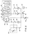
- developer unit 38 of an electrophotographic printing machine in which a belt 10 having a photoconductive surface 12 is moved in the direction of arrow 16 Electrostatic latent images on the belt 10 are developed by developer unit 38
- developer unit 38 includes a housing 66 defining a chamber 44 for storing a supply of developer material therein.
- Donor roller 40 , electrode wires 42 and magnetic roller 46 are mounted in chamber 44 of housing 66 .
- the donor roller can be rotated in either the 'with' or 'against' direction relative to the direction of motion of belt 10 .
- donor roller 40 is shown rotating in the direction of arrow 41 , i.e. the against direction.
- the magnetic roller can be rotated in either the 'with' or 'against' direction relative to the direction of motion of donor roller 40 .
- magnetic roller 46 is shown rotating in the direction of arrow 48 i.e. the against direction.
- Donor roller 40 is preferably overcoated with a layer of anodized aluminum.
- Other possible donor roll overcoatings include various polymers loaded with carbon black or graphite.
- Electrode wires 42 are disposed in the space between the belt 10 and donor roller 40 . Although only two wires are illustrated here for clarity, a plurality of electrode wires are typically used. The electrode wires are normally in intimate contact with donor roller 40 . A plurality, i.e.
- Each electrode wire extends in a direction substantially parallel to the longitudinal axis of the donor roller.
- Each electrode wire is made from a thin (i.e. 50 to 100 ⁇ m diameter) stainless steel strand.
- the extremities of the wires are supported by the tops of end bearing blocks which also support the donor roller for rotation.
- the wire extremities are attached so that they are tangential to and in contact with the surface of the donor roller. Mounting the wires in such a manner makes them insensitive to roll runout due to their self-spacing.
- an alternating electrical bias is applied to the electrode wires by an AC voltage source 90 .
- the applied AC establishes an alternating electrostatic field between the wires and the donor roller which is effective in detaching toner from the surtace of the donor roller and forming a toner cloud about the wires, the height of the cloud being such as not to be substantially in contact with the belt 10 .
- the applied A.C. is a biased waveform having a net DC component offset 89 causing the wire 42 to be more negatively charged on average than the donor roller.
- the bias keeps the electrode wires relatively free of negatively charged toner effecting an electrostatic cleaning.
- the AC voltage source 90 generates a balanced waveform with an average voltage of zero.
- the DC voltage source 89 whereby the AC source 90 "rides" an average D.C. bias according to the connection illustrated.
- the AC voltage source 90 itself may generate an unbalanced waveform with a non-zero average voltage.
- the non-zero average voltage alone or in combination with the DC source 89 is equivalent to the arrangement illustrated in FIGURE 1.
- An advantage of the present invention is that the electrode wires are electrostatically cleaned during application of the A.C. forming the toner cloud during the development operation. That is, the electrode wires are electrostatically cleaned on-thefly, rather than in an off-line process as in the past.
- the magnitude of the AC voltage is relatively low and is on the order of 200 to 600 volts peak at a frequency ranging from about 3 kHz to about 18 kHz.
- a DC bias supply 50 which applies approximately -350 volts to donor roller 40 establishes an electrostatic field between photoconductive surface 12 of belt 10 and donor roller 40 for attracting the detached toner particles from the cloud surrounding the wires to the latent image recorded on the photoconductive surface.
- the use of a dielectric coating on either the electrode wires or donor roller prevents shorting of the applied AC voltage.
- a cleaning blade 60 strips all of the toner from donor roller 40 after development so that magnetic roller 46 meters fresh toner to a clean donor roller. Magnetic roller 46 meters a constant quantity of toner having a substantially constant charge on to donor roller 40 .
- the donor roller provides a constant amount of toner having a substantially constant charge in the development gap.
- the combination of donor roller spacing, i.e. spacing between the donor roller and the magnetic roller, the compressed pile height of the developer material on the magnetic roller, and the magnetic properties of the magnetic roller in conjunction with the use of a conductive, magnetic developer material achieves the deposition of a constant quantity of toner having a substantially constant charge on the donor roller.
- DC bias supply 56 applies approximately -75 volts D.C.
- Magnetic roller 46 includes a non-magnetic tubular member or sleeve 52 made preferably from aluminum and having the exterior circumferential surface thereof roughened.
- An elongated multiple magnet 68 is positioned interiorly of and spaced from the tubular member The magnet is mounted stationarily.
- the tubular member is mounted on suitable bearings and is coupled to motor 64 for rotation thereby.
- the tubular member 52 rotates in the direction of arrow 48 to advance the developer material adhering thereto into the nip defined by donor roller 40 and magnetic roller 46 . Toner particles are attracted from the carrier granules on the magnetic roller to the donor roller. Scraper blade 58 moves denuded carrier granules on extraneous developer material from the surface of tubular member 52 .
- augers are located in chamber 44 of housing 66 .
- Augers 54 are mounted rotatably in chamber 44 to mix and transport developer material.
- the augers have blades extending spirally outwardly from a shaft. The blades are designed to advance the developer material in the axial direction substantially parallel to the longitudinal axis of the shaft.
- a toner dispenser (not shown) stores a supply of toner particles.
- the toner dispenser is in communication with chamber 44 of housing 66 .
- fresh toner particles are furnished to the developer material in the chamber from the toner dispenser.
- the augers in the chamber of the housing mix the fresh toner particles with the remaining developer material so that the resultant developer material therein is substantially uniform with the concentration of toner particles being optimized. In this way, a substantially constant amount of toner particles are in the chamber of the developer housing with the toner particles having a constant charge.
- the developer material in the chamber of the developer housing is magnetic and may be electrically conductive.
- the carrier granules include a ferromagnetic core with a non-continuous layer of resinous material.
- the toner particles are made from a resinous material, such as a vinyl polymer, mixed with a coloring material, such as carbon black.
- the developer material comprises from about 95% to about 99% by weight of carrier and from 5% to about 1% by weight of toner.
- any suitable developer material having at least carrier granules and toner particles may be used.
- FIGURE 2 there is shown the circuitry for electrostatic cleaning of electrode wires 42 using a D.C. bias according to the preterred embodiment.
- the DC voltages sources 50 , 56 shown in FIGURE 1 are illustrated here as being preferably a single first DC voltage source 100 with a polarity as indicated.
- the magnetic roller 46 is biased to be somewhat more negative than the donor roller 40 .
- a second DC voltage source 102 connects the magnetic roller 46 to the first DC voltage source 100 through a current limiting resistor 104 .
- the first DC voltage source 100 is set to -350 volts DC while the second DC voltage source 102 is set to -75 volts DC resulting in a bias on the donor roller 40 of -350 volts DC and a bias on the magnetic roller 46 of -425 volts DC.
- a first square wave AC voltage source 110 is connected to the magnetic roller 46 through a coupling capacitor 112 to influence a uniform deposit of development material onto the magnetic roller 46 from the chamber 44 .
- the magnetic roller 46 meters a constant quantity of toner having a substantially constant toner layer space charge of approximately -50 V to -75 V onto the donor roller 40 .
- a feature of the present invention is to provide the electrode wires 42 with an average electrostatic DC negative voltage offset with respect to the donor roller bias equal to the toner layer space charge level.
- the average DC negative voltage offset has been found to be approximately 25-150 volts and prererably about 50 volts. That is, for negatively charged contaminants, the electrode wires should be 50 volts more negative than the donor roller bias and equal to the toner layer space charge in the development gap. Of course, for positively charged contaminants, the electrode wires should be 50 volts more positive than the donor roller bias and equal to the toner layer space charge in the development gap.
- a second square wave AC voltage source 120 is capacitively coupled to the electrode wires 42 through a coupling capacitor 122 and a current limiting resistor 124 .
- the applied AC from the second square wave AC voltage source 120 establishes an alternating electrostatic field between the wires 42 and the donor roller 40 which is effective is detaching toner form the surface of the donor roller and forming a toner cloud about the wires 42 in the development gap.
- a third DC voltage source 130 is connected in parallel with the second square wave AC voltage source 120 through a current limiting resistor 132 .
- the third DC voltage source 130 is set to between -50 volts DC and -75 volts DC to effect a difference in potential between the wires 42 and the donor roller 40 of approximately 50 to 75 volts. This has been found to effectively eliminate the accumulation of toner build-up on the wires 42 which is a major cause of both ghosting and streaks in the developed image.
- two power supplies 120 , 130 are illustrated, it is possible to provide a single AC voltage which includes a biased waveform having a net DC component offset causing the electrode wires to be more negatively charged on average than the donor roller.
- the donor roller 40 is substantially cleaned of toner between print cycles or off-line by adjusting the DC bias on variable supplies 102 and/or 100 such that toner particles are electrostatically driven to move from the donor roller surface back onto the carrier granules.
- the small amount of toner remaining on the donor roller is typically of opposite polarity from the toner used for development of the latent image.
- the space charge of this toner on the donor roller during this off-line donor cleaning cycle is positive.
- the DC bias 130 applied to the electrodes 42 is changed to approximately positive 20 to 150 volts relative to the donor roller to prevent toner build-up on the wires.
- the electrostatic attraction of the electrode to the donor roller is reduced and the electrode vibration is thereby reduced.
- a first sinusoidal wave AC voltage source 140 is connected between the donor roller 40 and the first DC voltage source 100 through a transformer 142 .
- This voltage source may be included as desired to control the developability of lines in the degree of interaction between the toner and the receiver as taught in US-A-5,010,367 to Hays.
- the development system of the present invention includes an electrostatic negative DC offset on the electrode wires positioned closely adjacent the exterior surface of a more positively biased donor roll in the gap defining the development zone between the donor roll and the photoconductive belt.
- An electrostatic field is generated between the electrode wires and the donor roll whereby the electrostatic field discourages build-up of toner particles on the development wires.
- An average negative DC voltage is applied to the electrode wires to generate an electrostatic field thereon.
- the electrostatic field in combination with the charge on the donor roller substantially reduces the build-up of negatively charged toner on the electrode wires.
Landscapes
- Physics & Mathematics (AREA)
- General Physics & Mathematics (AREA)
- Dry Development In Electrophotography (AREA)
- Developing For Electrophotography (AREA)
- Cleaning In Electrography (AREA)
Claims (10)
- Dispositif de formation d'image destiné à former des images sur une surface de réception d'image (10, 12) à l'aide d'un dispositif de développement, le dispositif comprenant :caractérisé en ce queune réserve (38) de particules de marquage,un moyen de transport (40) destiné à transporter des particules de marquage depuis la réserve (38) jusqu'à une zone voisine de la surface de réception d'image (10, 12),une structure de filaments d'électrode (42) disposée entre le moyen de transport (40) et la surface de réception d'image (10, 12) afin de former un nuage de particules de marquage transportées, etune source de tension en courant alternatif (120) destinée à appliquer un potentiel de tension alternatif à la structure de filaments d'électrode (42) par rapport au moyen de transport (40),
d'autres moyens électrostatiques (122, 124, 130, 132) destinés à nettoyer la structure de filaments d'électrode (42) en créant en plus un potentiel de tension électrostatique moyen sur la structure de filaments d'électrode (42) par rapport au moyen de transport (40) sont prévus et reliés de façon qu'en utilisation, un potentiel de tension électrostatique moyen soit créé sur la structure de filaments d'électrode (42) par rapport au moyen de transport (40) en appliquant un signal de tension de décalage à au moins l'une parmi la structure de filaments d'électrode (42) et la source de tension en courant alternatif (120). - Dispositif selon la revendication 1, dans lequel la source de tension (120) comprend une source de tension en courant alternatif à signaux carrés.
- Dispositif selon la revendication 1 ou 2, dans lequel le moyen de transport (40) comprend un rouleau donneur destiné à transporter lesdites particules de marquage depuis ladite réserve (38) jusqu'à ladite zone à proximité de la surface de réception d'image (10, 12), les particules transportées accumulant un potentiel de tension de charge d'espace d'une polarité donnée, et le signal de tension moyenne de décalage polarise la structure de filaments d'électrode (42) à la polarité donnée par rapport au rouleau donneur.
- Dispositif selon la revendication 3, dans lequel le décalage de tension en courant continu électrostatique moyen appliqué aux filaments d'électrode (42) par rapport au rouleau donneur est égal à la charge d'espace de la couche de toner dans l'interstice de développement.
- Procédé de nettoyage d'une structure de filaments d'électrode (42) dans un dispositif de formation d'image selon l'une quelconque des revendications précédentes, le procédé consistant à
polariser la structure de filaments d'électrode (42) à l'aide d'un signal de tension électrostatique en courant alternatif par rapport au moyen de transport (40),
caractérisé en ce que
la structure de filaments d'électrode (42) est en outre polarisée à l'aide d'un signal de tension en courant continu électrostatique moyen par rapport au moyen de transport (40) afin de repousser les particules de marquage à l'écart de la structure de filaments d'électrode (42). - Procédé selon la revendication 5, dans lequel
la tension en courant continu électrostatique moyenne qui polarise la structure de filaments d'électrode (42) par rapport au rouleau donneur (40) est établie à la polarité donnée par le potentiel de tension de charge d'espace qui est accumulé par les particules de marquage transportées par le moyen de transport (40). - Procédé selon la revendication 5, dans lequel
le décalage de tension en courant continu électrostatique moyen entre la structure de filaments d'électrode (42) et le moyen de transport (40) est négatif. - Procédé selon la revendication 5, 6 ou 7, dans lequel
la structure de filaments d'électrode (42) est polarisée à l'aide d'un signal de tension en courant alternatif à signaux carrés présentant une composante de tension en courant continu négative par rapport au moyen de transport (40). - Procédé selon la revendication 8, dans lequel
le signal de tension en courant alternatif à signaux carrés et le signal de tension en courant continu négative sont appliqués en permanence à la structure de filaments d'électrode (42) pendant le développement de l'image latente sur la surface de réception (10, 12). - Procédé selon la revendication 8, comprenant, entre des cycles de développement, l'étape consistant à polariser électriquement la structure de filaments d'électrode (42) à l'aide d'un signal de tension présentant une composante de tension électrostatique moyenne par rapport au moyen de transport (40) afin de détacher du toner de celle-ci.
Applications Claiming Priority (2)
| Application Number | Priority Date | Filing Date | Title |
|---|---|---|---|
| US110460 | 1993-08-23 | ||
| US08/110,460 US5311258A (en) | 1993-08-23 | 1993-08-23 | On-the-fly electrostatic cleaning of scavengeless development electrode wires with D.C. bias |
Publications (3)
| Publication Number | Publication Date |
|---|---|
| EP0640887A2 EP0640887A2 (fr) | 1995-03-01 |
| EP0640887A3 EP0640887A3 (fr) | 1995-05-10 |
| EP0640887B1 true EP0640887B1 (fr) | 1999-08-04 |
Family
ID=22333132
Family Applications (1)
| Application Number | Title | Priority Date | Filing Date |
|---|---|---|---|
| EP94305840A Expired - Lifetime EP0640887B1 (fr) | 1993-08-23 | 1994-08-05 | Nettoyage électrostatique avec tension continue pour les filaments non abrasés d'électrode |
Country Status (4)
| Country | Link |
|---|---|
| US (1) | US5311258A (fr) |
| EP (1) | EP0640887B1 (fr) |
| JP (1) | JP3466719B2 (fr) |
| DE (1) | DE69419850T2 (fr) |
Families Citing this family (22)
| Publication number | Priority date | Publication date | Assignee | Title |
|---|---|---|---|---|
| US5499084A (en) * | 1994-03-14 | 1996-03-12 | Xerox Corporation | Development system for use in a color printer |
| US5734954A (en) * | 1996-05-07 | 1998-03-31 | Xerox Corporation | Hybrid scavengeless development using a power supply controller to prevent toner contamination |
| KR0174689B1 (ko) * | 1996-09-11 | 1999-04-01 | 삼성전자주식회사 | 현상롤러의 고스트 방지장치 |
| US5787329A (en) * | 1997-04-29 | 1998-07-28 | Xerox Corporation | Organic coated development electrodes and methods thereof |
| US5778290A (en) * | 1997-04-29 | 1998-07-07 | Xerox Corporation | Composite coated development electrodes and methods thereof |
| US5848327A (en) * | 1997-04-29 | 1998-12-08 | Xerox Corporation | Coating compositions for development electrodes and methods thereof |
| US5761587A (en) * | 1997-04-29 | 1998-06-02 | Xerox Corporation | Coated development electrodes and methods thereof |
| US5805964A (en) * | 1997-04-29 | 1998-09-08 | Xerox Corporation | Inorganic coated development electrodes and methods thereof |
| US5864734A (en) * | 1997-07-21 | 1999-01-26 | Xerox Corporation | Development system producing reduced airborne toner contamination |
| US6049686A (en) * | 1998-10-02 | 2000-04-11 | Xerox Corporation | Hybrid scavengeless development using an apparatus and a method for preventing wire contamination |
| US6198886B1 (en) | 1999-08-12 | 2001-03-06 | Xerox Corporation | Method and apparatus comprising process control for scavengeless development in a xerographic printer |
| US6201936B1 (en) | 1999-12-03 | 2001-03-13 | Xerox Corporation | Method and apparatus for adaptive black solid area estimation in a xerographic apparatus |
| US7340204B2 (en) * | 2004-10-25 | 2008-03-04 | Ricoh Company, Ltd. | Color image forming apparatus and process cartridge therefor |
| JP4234667B2 (ja) * | 2004-11-30 | 2009-03-04 | 株式会社東芝 | 移動体用ofdm受信装置 |
| US7312010B2 (en) * | 2005-03-31 | 2007-12-25 | Xerox Corporation | Particle external surface additive compositions |
| US7862970B2 (en) * | 2005-05-13 | 2011-01-04 | Xerox Corporation | Toner compositions with amino-containing polymers as surface additives |
| US7754408B2 (en) | 2005-09-29 | 2010-07-13 | Xerox Corporation | Synthetic carriers |
| DE102007035994A1 (de) * | 2007-08-01 | 2009-02-05 | OCé PRINTING SYSTEMS GMBH | Vorrichtung und Verfahren zum Beseitigen von Tonerablagerungen auf der Oberfläche eines Reinigungselements |
| JP5177649B2 (ja) * | 2008-05-21 | 2013-04-03 | 株式会社リコー | 現像装置、プロセスユニット及び画像形成装置 |
| JP5354370B2 (ja) * | 2009-09-14 | 2013-11-27 | 株式会社リコー | 現像装置及び画像形成装置 |
| JP2012118261A (ja) * | 2010-11-30 | 2012-06-21 | Ricoh Co Ltd | 現像装置、プロセスカートリッジ、及び、画像形成装置 |
| US8750769B2 (en) * | 2012-04-23 | 2014-06-10 | Xerox Corporation | Inferring toner contamination of electrodes from printing parameters |
Family Cites Families (14)
| Publication number | Priority date | Publication date | Assignee | Title |
|---|---|---|---|---|
| JPS58135752U (ja) * | 1982-03-05 | 1983-09-12 | ティーディーケイ株式会社 | 静電式複写機用帯電装置 |
| US4568955A (en) * | 1983-03-31 | 1986-02-04 | Tokyo Shibaura Denki Kabushiki Kaisha | Recording apparatus using a toner-fog generated by electric fields applied to electrodes on the surface of the developer carrier |
| US5010367A (en) * | 1989-12-11 | 1991-04-23 | Xerox Corporation | Dual AC development system for controlling the spacing of a toner cloud |
| US4984019A (en) * | 1990-02-26 | 1991-01-08 | Xerox Corporation | Electrode wire cleaning |
| US5063875A (en) * | 1990-03-19 | 1991-11-12 | Xerox Corporation | Development apparatus having a transport roll rotating at least twice the surface velocity of a donor roll |
| US5053824A (en) * | 1990-04-16 | 1991-10-01 | Xerox Corporation | Scavengeless development apparatus having a donor belt |
| US5134442A (en) * | 1990-07-26 | 1992-07-28 | Xerox Corporation | Electrode wire contamination prevention and detection |
| US5212037A (en) * | 1991-08-01 | 1993-05-18 | Xerox Corporation | Toner process with metal oxides |
| US5144371A (en) * | 1991-08-02 | 1992-09-01 | Xerox Corporation | Dual AC/dual frequency scavengeless development |
| US5124749A (en) * | 1991-09-13 | 1992-06-23 | Xerox Corporation | Damping electrode wires of a developer unit |
| US5144370A (en) * | 1991-10-31 | 1992-09-01 | Xerox Corporation | Apparatus for detecting the vibration of electrode wires and canceling the vibration thereof |
| US5204719A (en) * | 1992-02-10 | 1993-04-20 | Xerox Corporation | Development system |
| US5153648A (en) * | 1992-03-02 | 1992-10-06 | Xerox Corporation | Electrode wire mounting for scavengeless development |
| US5172170A (en) * | 1992-03-13 | 1992-12-15 | Xerox Corporation | Electroded donor roll for a scavengeless developer unit |
-
1993
- 1993-08-23 US US08/110,460 patent/US5311258A/en not_active Expired - Lifetime
-
1994
- 1994-08-05 DE DE69419850T patent/DE69419850T2/de not_active Expired - Lifetime
- 1994-08-05 EP EP94305840A patent/EP0640887B1/fr not_active Expired - Lifetime
- 1994-08-11 JP JP18958194A patent/JP3466719B2/ja not_active Expired - Fee Related
Also Published As
| Publication number | Publication date |
|---|---|
| JP3466719B2 (ja) | 2003-11-17 |
| US5311258A (en) | 1994-05-10 |
| EP0640887A3 (fr) | 1995-05-10 |
| DE69419850D1 (de) | 1999-09-09 |
| JPH0784450A (ja) | 1995-03-31 |
| DE69419850T2 (de) | 1999-11-25 |
| EP0640887A2 (fr) | 1995-03-01 |
Similar Documents
| Publication | Publication Date | Title |
|---|---|---|
| EP0640887B1 (fr) | Nettoyage électrostatique avec tension continue pour les filaments non abrasés d'électrode | |
| US4984019A (en) | Electrode wire cleaning | |
| US5172170A (en) | Electroded donor roll for a scavengeless developer unit | |
| USRE35698E (en) | Donor roll for scavengeless development in a xerographic apparatus | |
| EP0426420B1 (fr) | Appareil de développement | |
| EP0601786B1 (fr) | Bon chargement d'un rouleau donneur en développement hybride | |
| EP0414455A2 (fr) | Système de développement hybride | |
| US5592271A (en) | Donor rolls with capacitively cushioned commutation | |
| EP0571117B1 (fr) | ContrÔle des impuretés pour le développement sans contact dans un appareil xérographique | |
| JP3238531B2 (ja) | 画像形成装置及び方法 | |
| US5517287A (en) | Donor rolls with interconnected electrodes | |
| US4990958A (en) | Reload member for a single component development housing | |
| US5134442A (en) | Electrode wire contamination prevention and detection | |
| US5144370A (en) | Apparatus for detecting the vibration of electrode wires and canceling the vibration thereof | |
| US6668146B2 (en) | Hybrid scavengeless development using direct current voltage shift to remove wire history | |
| US5422709A (en) | Electrode wire grid for developer unit | |
| US5053824A (en) | Scavengeless development apparatus having a donor belt | |
| US5515142A (en) | Donor rolls with spiral electrodes for commutation | |
| US20030228177A1 (en) | Apparatus and method for reducing ghosting defects in a printing machine | |
| US5204719A (en) | Development system | |
| US5523826A (en) | Developer units with residual toner removal to assist reloading | |
| US5742885A (en) | Development system employing acoustic toner fluidization for donor roll | |
| US5761587A (en) | Coated development electrodes and methods thereof | |
| US6631250B2 (en) | Developer filtration module | |
| US5499084A (en) | Development system for use in a color printer |
Legal Events
| Date | Code | Title | Description |
|---|---|---|---|
| PUAI | Public reference made under article 153(3) epc to a published international application that has entered the european phase |
Free format text: ORIGINAL CODE: 0009012 |
|
| AK | Designated contracting states |
Kind code of ref document: A2 Designated state(s): DE FR GB |
|
| PUAL | Search report despatched |
Free format text: ORIGINAL CODE: 0009013 |
|
| RHK1 | Main classification (correction) |
Ipc: G03G 15/095 |
|
| AK | Designated contracting states |
Kind code of ref document: A3 Designated state(s): DE FR GB |
|
| 17P | Request for examination filed |
Effective date: 19951110 |
|
| 17Q | First examination report despatched |
Effective date: 19970128 |
|
| GRAG | Despatch of communication of intention to grant |
Free format text: ORIGINAL CODE: EPIDOS AGRA |
|
| GRAG | Despatch of communication of intention to grant |
Free format text: ORIGINAL CODE: EPIDOS AGRA |
|
| GRAH | Despatch of communication of intention to grant a patent |
Free format text: ORIGINAL CODE: EPIDOS IGRA |
|
| GRAH | Despatch of communication of intention to grant a patent |
Free format text: ORIGINAL CODE: EPIDOS IGRA |
|
| GRAA | (expected) grant |
Free format text: ORIGINAL CODE: 0009210 |
|
| AK | Designated contracting states |
Kind code of ref document: B1 Designated state(s): DE FR GB |
|
| REF | Corresponds to: |
Ref document number: 69419850 Country of ref document: DE Date of ref document: 19990909 |
|
| ET | Fr: translation filed | ||
| PLBE | No opposition filed within time limit |
Free format text: ORIGINAL CODE: 0009261 |
|
| STAA | Information on the status of an ep patent application or granted ep patent |
Free format text: STATUS: NO OPPOSITION FILED WITHIN TIME LIMIT |
|
| 26N | No opposition filed | ||
| REG | Reference to a national code |
Ref country code: GB Ref legal event code: IF02 |
|
| REG | Reference to a national code |
Ref country code: GB Ref legal event code: 746 Effective date: 20050512 |
|
| PGFP | Annual fee paid to national office [announced via postgrant information from national office to epo] |
Ref country code: FR Payment date: 20090814 Year of fee payment: 16 |
|
| PGFP | Annual fee paid to national office [announced via postgrant information from national office to epo] |
Ref country code: GB Payment date: 20090805 Year of fee payment: 16 Ref country code: DE Payment date: 20090730 Year of fee payment: 16 |
|
| GBPC | Gb: european patent ceased through non-payment of renewal fee |
Effective date: 20100805 |
|
| REG | Reference to a national code |
Ref country code: FR Ref legal event code: ST Effective date: 20110502 |
|
| REG | Reference to a national code |
Ref country code: DE Ref legal event code: R119 Ref document number: 69419850 Country of ref document: DE Effective date: 20110301 |
|
| PG25 | Lapsed in a contracting state [announced via postgrant information from national office to epo] |
Ref country code: DE Free format text: LAPSE BECAUSE OF NON-PAYMENT OF DUE FEES Effective date: 20110301 Ref country code: FR Free format text: LAPSE BECAUSE OF NON-PAYMENT OF DUE FEES Effective date: 20100831 |
|
| PG25 | Lapsed in a contracting state [announced via postgrant information from national office to epo] |
Ref country code: GB Free format text: LAPSE BECAUSE OF NON-PAYMENT OF DUE FEES Effective date: 20100805 |