EP0640480A2 - Ink jet printer head and a method of driving the same - Google Patents
Ink jet printer head and a method of driving the same Download PDFInfo
- Publication number
- EP0640480A2 EP0640480A2 EP94306314A EP94306314A EP0640480A2 EP 0640480 A2 EP0640480 A2 EP 0640480A2 EP 94306314 A EP94306314 A EP 94306314A EP 94306314 A EP94306314 A EP 94306314A EP 0640480 A2 EP0640480 A2 EP 0640480A2
- Authority
- EP
- European Patent Office
- Prior art keywords
- pressure chamber
- side walls
- electrodes
- pressure chambers
- ink
- Prior art date
- Legal status (The legal status is an assumption and is not a legal conclusion. Google has not performed a legal analysis and makes no representation as to the accuracy of the status listed.)
- Granted
Links
Images


Classifications
-
- B—PERFORMING OPERATIONS; TRANSPORTING
- B41—PRINTING; LINING MACHINES; TYPEWRITERS; STAMPS
- B41J—TYPEWRITERS; SELECTIVE PRINTING MECHANISMS, i.e. MECHANISMS PRINTING OTHERWISE THAN FROM A FORME; CORRECTION OF TYPOGRAPHICAL ERRORS
- B41J2/00—Typewriters or selective printing mechanisms characterised by the printing or marking process for which they are designed
- B41J2/005—Typewriters or selective printing mechanisms characterised by the printing or marking process for which they are designed characterised by bringing liquid or particles selectively into contact with a printing material
- B41J2/01—Ink jet
- B41J2/015—Ink jet characterised by the jet generation process
- B41J2/04—Ink jet characterised by the jet generation process generating single droplets or particles on demand
- B41J2/045—Ink jet characterised by the jet generation process generating single droplets or particles on demand by pressure, e.g. electromechanical transducers
- B41J2/04501—Control methods or devices therefor, e.g. driver circuits, control circuits
- B41J2/04581—Control methods or devices therefor, e.g. driver circuits, control circuits controlling heads based on piezoelectric elements
-
- B—PERFORMING OPERATIONS; TRANSPORTING
- B41—PRINTING; LINING MACHINES; TYPEWRITERS; STAMPS
- B41J—TYPEWRITERS; SELECTIVE PRINTING MECHANISMS, i.e. MECHANISMS PRINTING OTHERWISE THAN FROM A FORME; CORRECTION OF TYPOGRAPHICAL ERRORS
- B41J2/00—Typewriters or selective printing mechanisms characterised by the printing or marking process for which they are designed
- B41J2/005—Typewriters or selective printing mechanisms characterised by the printing or marking process for which they are designed characterised by bringing liquid or particles selectively into contact with a printing material
- B41J2/01—Ink jet
- B41J2/015—Ink jet characterised by the jet generation process
- B41J2/04—Ink jet characterised by the jet generation process generating single droplets or particles on demand
- B41J2/045—Ink jet characterised by the jet generation process generating single droplets or particles on demand by pressure, e.g. electromechanical transducers
- B41J2/04501—Control methods or devices therefor, e.g. driver circuits, control circuits
- B41J2/04588—Control methods or devices therefor, e.g. driver circuits, control circuits using a specific waveform
-
- B—PERFORMING OPERATIONS; TRANSPORTING
- B41—PRINTING; LINING MACHINES; TYPEWRITERS; STAMPS
- B41J—TYPEWRITERS; SELECTIVE PRINTING MECHANISMS, i.e. MECHANISMS PRINTING OTHERWISE THAN FROM A FORME; CORRECTION OF TYPOGRAPHICAL ERRORS
- B41J2/00—Typewriters or selective printing mechanisms characterised by the printing or marking process for which they are designed
- B41J2/005—Typewriters or selective printing mechanisms characterised by the printing or marking process for which they are designed characterised by bringing liquid or particles selectively into contact with a printing material
- B41J2/01—Ink jet
- B41J2/015—Ink jet characterised by the jet generation process
- B41J2/04—Ink jet characterised by the jet generation process generating single droplets or particles on demand
- B41J2/045—Ink jet characterised by the jet generation process generating single droplets or particles on demand by pressure, e.g. electromechanical transducers
- B41J2/04501—Control methods or devices therefor, e.g. driver circuits, control circuits
- B41J2/04593—Dot-size modulation by changing the size of the drop
-
- B—PERFORMING OPERATIONS; TRANSPORTING
- B41—PRINTING; LINING MACHINES; TYPEWRITERS; STAMPS
- B41J—TYPEWRITERS; SELECTIVE PRINTING MECHANISMS, i.e. MECHANISMS PRINTING OTHERWISE THAN FROM A FORME; CORRECTION OF TYPOGRAPHICAL ERRORS
- B41J2/00—Typewriters or selective printing mechanisms characterised by the printing or marking process for which they are designed
- B41J2/005—Typewriters or selective printing mechanisms characterised by the printing or marking process for which they are designed characterised by bringing liquid or particles selectively into contact with a printing material
- B41J2/01—Ink jet
- B41J2/135—Nozzles
- B41J2/14—Structure thereof only for on-demand ink jet heads
- B41J2002/14491—Electrical connection
-
- B—PERFORMING OPERATIONS; TRANSPORTING
- B41—PRINTING; LINING MACHINES; TYPEWRITERS; STAMPS
- B41J—TYPEWRITERS; SELECTIVE PRINTING MECHANISMS, i.e. MECHANISMS PRINTING OTHERWISE THAN FROM A FORME; CORRECTION OF TYPOGRAPHICAL ERRORS
- B41J2202/00—Embodiments of or processes related to ink-jet or thermal heads
- B41J2202/01—Embodiments of or processes related to ink-jet heads
- B41J2202/10—Finger type piezoelectric elements
Definitions
- the present invention relates to a drop-on-demand ink jet print head mounted on an ink jet printer and a method of driving the same.
- Fig. 1 shows a passage (a pressure chamber) having a hard wall on one side and a shearing strain actuator wall on the other side.
- the shearing strain actuator wall consists of piezoelectric ceramic. An upper portion and a lower portion of these walls are joined to each other on their boundary surfaces thereof. They are also fixedly joined to a top wall and a bottom wall.
- Metallized metal electrodes are formed on surfaces of the both walls of the shearing strain actuator disposed on one side of the two side walls.
- the actuator wall is deformed toward the passage and thus pressure is provided to ink throughout the entire length of the passage, as a shearing deformation is caused in the piezoelectric ceramic by applying a pulse voltage between the electrodes. If the pressure against the ink thus applied is beyond the predetermined minimum value, the ink is jetted is extracted through a nozzle.
- Fig. 9 (a) in the above mentioned Laid-open discloses the ink jet print head having a pair of shearing strain actuators formed on both sides of passage walls.
- An upper and lower portions of the passage consist of a top wall and a bottom wall.
- Electrodes of the actuators are formed on an inner surface of the passage and two surfaces on outside of both walls of the passage in the form of metal electrodes.
- Laid-open also describes that the size of an ink droplet can be controlled by changing the voltage to be applied.
- the ink jet print head which jets ink by driving an actuator formed on one side of a passage (pressure chamber), and the ink jet print head which jets ink by simultaneously changing similar actuators respectively formed on both sides of a passage.
- pressure variation in a pressure chamber is utilized by changing the voltage to be applied in order to change the size of a droplet. Therefore, the same number of voltages to be applied as the number of gradation degrees is required.
- an apparatus to switch a connection of a plurality of electric sources corresponding to the gradation degrees and electrodes of each actuator is required which is costly.
- a first object of the present invention in the graphic printing is to provide an ink jet print head and a method of driving the same which perform gradation with a simply constructed device.
- a second object of the present invention is to provide an ink jet print head and a method of driving the same which perform gradation in the graphic printing by a unique control.
- a third object of the present invention is to provide an ink jet print head and a method of driving the same which perform gradation in the graphic printing without changing the structure of device as compared with conventional ink jet print head and a method of driving the same.
- a fourth object of the present invention is to provide an ink jet print head and a method of driving the same which perform gradation in the graphic printing at a low cost.
- An ink jet print head has a plurality of pressure chambers and electrodes, ink jets and driving units corresponding to the pressure chambers.
- Pressure chambers are divided by side walls at least partially formed of a piezoelectric member.
- the electrodes are formed on surfaces of the side walls such that they contact the piezoelectric member in the pressure chambers.
- Ink jets are formed to communicate with the pressure chambers so as to jet ink in the pressure chambers.
- a control unit applies voltage to an electric source to deform the side walls in shearing strain mode thereby to jet the ink through the ink jets.
- the piezoelectric member is driven such that voltage to be applied to the electrode corresponding to one side walls and to the other side walls of the pressure chamber differ.
- pressure in the pressure chamber varies in three ways, i.e., 1) when driving only one side wall of the pressure chamber, 2) when driving only the other side walls of the pressure chamber, and 3) when driving both side walls of the pressure chambers.
- the size of the droplet can be controlled by changing the pressure in the pressure chambers as mentioned above. Therefore, the gradation can be readily acquired only by setting two driving voltage values.
- An ink jet print head has a plurality of pressure chambers and electrodes, ink jets and driving units corresponding to the pressure chambers.
- Pressure chambers are divided by side walls at least partially formed of a piezoelectric member. Each side wall formed on both sides of the pressure chamber has different operating characteristic of shearing strain mode.
- the electrodes are formed on the surfaces of the side walls so that they contact the piezoelectric member in the pressure chamber.
- Ink jets are formed communicating with the pressure chambers so as to jet ink in the pressure chambers.
- a control unit applies voltage to an electric source to deform the side walls in shearing strain mode and to drive the piezoelectric member thereby to jet the ink in the pressure chamber through the ink jets.
- pressure in the pressure chambers varies in three ways, i.e., 1) when driving only one side walls of the pressure chambers, 2) when driving only the other side walls of the pressure chambers, and 3) when driving both side walls of the pressure chambers.
- the size of the droplet can be controlled by changing the pressure in the pressure chamber as mentioned above. Therefore, gradation can be readily acquired by setting a driving voltage value.
- a method of driving an ink jet print head uses the ink jet print head comprising a plurality of pressure chambers and electrodes, ink jets and driving units corresponding to the pressure chambers.
- Pressure chambers are divided by side walls at least partially formed of a piezoelectric member.
- the electrodes are formed on side wall surfaces such that they contact the piezoelectric member in the pressure chambers.
- Ink jets are formed communicating with the pressure chambers so as to jet ink in the pressure chambers.
- a control unit applies voltage to an electric source to deform the side walls in shearing strain mode and to drive the piezoelectric member thereby to jet the ink through the ink jets.
- the voltage to be applied to the electrodes can be varied in every pressure chamber in three ways, i.e., 1) when deforming only one side wall of the pressure chamber, 2) when deforming only the other side wall of the pressure chamber, and 3) when deforming both side walls of the pressure chamber.
- the size of the droplet can be controlled by changing the pressure in the pressure chamber as mentioned above. Therefore, gradation can be readily acquired.
- a method of driving an ink jet print head uses the ink jet print head comprising a plurality of pressure chambers and electrodes, ink jets and driving units corresponding to the pressure chambers.
- the pressure chambers are divided by side walls at least partially formed of a piezoelectric member.
- the electrodes are formed on surfaces of the side walls such that they contact the piezoelectric member in the pressure chambers.
- Ink jets are formed communicating with the pressure chambers so as to jet ink in the pressure chambers.
- a control unit applies voltage to an electric source to deform the side walls in shearing strain mode and to drive the piezoelectric member thereby to jet the ink through the ink jets.
- the electrodes are alternately connected to two electric sources having different voltage in every two pressure chambers. Accordingly, the pressure in the pressure chambers varies in three ways when the voltage is applied to 1) the electrodes on one side of the pressure chambers, 2) to the electrodes on the other side of the pressure chambers or 3) to the electrodes on both sides of the pressure chambers to change the size of the droplets, as well as earthing the electrodes in the pressure chambers from which droplet is to be jetted. Therefore, gradation can be readily acquired.
- a method of driving an ink jet print head uses the ink jet print head comprising a plurality of pressure chambers and electrodes, ink jets and driving units corresponding to the pressure chambers.
- Pressure chambers are divided by side walls at least partially formed of a piezoelectric member.
- the electrodes are formed on surfaces of the side walls such that they contact the piezoelectric member in the pressure chambers.
- Ink jets are formed communicating with the pressure chambers so as to jet ink in the pressure chambers.
- a control unit applies voltage to an electric source to deform the side walls in shearing strain mode and to drive the piezoelectric member thereby to jet the ink through the ink jet outlets.
- Fig. 1 is a longitudinal sectional rear views of an ink jet print head including driving circuits according to a first embodiment of the present invention.
- Fig. 2 is a timing chart showing status of voltage applied to electrodes.
- Fig. 3(A) is a sectional view of ink jet illustrating a status of ink held by surface tension.
- Fig. 3(B) is a sectional view of an ink jet illustrating status of ink when pressure in pressure chamber is reduced.
- Fig. 3(C) is a sectional view of the ink jet illustrating status of ink resulting from the status shown in Fig. 3(B) when the pressure is increased in the pressure chamber.
- Fig. 3(D) is a sectional view of the ink jet illustrating status of ink resulting from the status shown in Fig. 3(C) when an ink droplet is grown.
- Fig. 3(E) is a sectional view of the ink jet illustrating status of the ink droplet having a pinch resulting from the status shown in Fig. 3(D) .
- Fig. 3(F) is a sectional view of the ink jet outlet illustrating status of ink resulting from the status shown in Fig. 3(E) when the ink droplet is jetted.
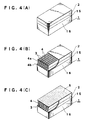
- Fig. 4(A) is a perspective view illustrating a fabricating step (a).
- Fig. 4 (B) is a perspective view illustrating a fabricating step (b) for forming grooves by grinding and a fabricating step (c) for implementing a pretreatment for electroless plating.
- Fig. 4(C) is a perspective view illustrating a fabricating step (d) for forming a mask over a piezoelectric member.
- Fig. 5(A) is a perspective view illustrating a fabricating step (e) for implementing an exposure and development process with a resist mask placed on the piezoelectric member.
- Fig. 5(B) is a perspective view illustrating a fabricating step (e) when the exposure and development process is finished.
- Fig. 6(A) is a perspective view illustrating a fabricating step (f) for electroless plating.
- Fig. 6(B) is a perspective view illustrating a fabricating step (g) for peeling off the resist film.
- Fig. 6(C) is a perspective view illustrating a fabricating step (g) when the all the steps are finished and an ink jet print head is completed.
- Fig. 7 is a longitudinal sectional rare view of an ink jet print head including driving circuits according to a second embodiment of the present invention.
- Fig. 8 is a timing chart showing status of voltage applied to electrodes.
- a first embodiment of the present invention will be described hereinafter with reference to Fig. 1 to Fig. 6.
- a structure of an ink jet print head according to the present invention will be described with reference to Fig. 4 to Fig. 6 in order of fabricating steps thereof.
- a base plate 1 is formed as shown in Fig. 4(A) by coating a resin adhesive containing as a principal component an epoxy resin having a high bonding strength over a bottom plate 16 of aluminum or glass having a high rigidity and a low thermal deformation.
- a piezoelectric member 2 polarized in the direction of its thickness is put on the adhesive. Then, the bottom plate 16, bottom layer 15 consisting of the adhesive and the piezoelectric member 2 are joined together to form three overlapped layers by hardening the adhesive.
- a plurality of parallel grooves 3 are formed at predetermined intervals through the surface of the piezoelectric member 2 into the bottom layer 15 by grinding.
- This also forms side walls 4 on both sides of the grooves 3.
- the side walls 4 consist of an upper side wall 4a formed of the piezoelectric member and a lower side wall 4b formed of the bottom layer 15 having lower rigidity than that of the piezoelectric member 2.
- the base plate 1 is then subject to washing, catalyzing and accelerating treatment as a pretreatment before forming electrodes by electroless plating.
- the base plate 1 is washed to activate plated surfaces and to make it hydrophilic such that catalyzing liquid, accelerating liquid and plating liquid can readily flow into the grooves 3.
- Catalyzing treatment is carried out to adsorb Pd-Sn complex on inner surfaces of the grooves 3 by immersing the base plate 1 in the catalyzing liquid used as pretreatment liquid , containing Palladium chloride, Stannous chloride, concentrated Sulfuric acid and the like.
- Pd-Sn complex is deposited on the surfaces of upper side walls 4a and lower walls 4b forming each groove 3.
- Accelerating treatment is carried out to catalyze the complex deposited by catalyzing treatment such that the complex deposited on the side walls 4 becomes metallized Pd, i.e., a catalyst core.
- a mask is formed over the surface of the piezoelectric member 2. This is carried out by putting a dry film 5 on the surface of the piezoelectric member 2 as shown in Fig. 4(C).
- a resist mask 6 is placed on the dry film 5 excluding portions in which a wiring pattern to be formed as shown in Fig. 5(A). Then, the dry film 5 is exposed to light and subject to development. Consequently, as shown in Fig. 5(B), resist film 7 formed with the dry film 5 remains over the surface of the piezoelectric member 2 excluding portions in which the wiring pattern is to be formed. Therefore, the metallized Pd is exposed on the wiring pattern of the piezoelectric member 2 and on the inner surface of the grooves 3.
- the base plate 1 is immersed in a plating bath for electroless plating.
- the plating bath contains a metallic salt and a reducing agent as principal components and additives such as a pH regulator, a buffer, a complexing agent, an accelerator, a stabilizer and a modifier.
- a plate is formed around metallized Pd used as a catalyst core thereby forming electrodes 8 on the surface of the grooves 3 in the side walls 4 and on the wiring pattern 9 communicating with the electrodes 8 on the piezoelectric member 2 shown in Fig 6(A).
- the resist film 7 placed on the surface of the piezoelectric member 2 is peeled off as shown in Fig. 6(B). Then, a top plate 10 is attached to the surface of the piezoelectric member 2 at which the plurality of parallel grooves 3 are formed and a nozzle plate 12 having ink jets 11 formed thereon is fixedly attached to the side surface of the base plate 1 and the top plate 10. The ink jets 11 are communicating with the tips of the each groove 3. As shown in Fig. 1, the grooves 3 are closed by the top plate 10 to form pressure chambers 14. Before attaching the nozzle plate 12, side surfaces of the base plate 1 and the top plate 10 on which the nozzle plate 12 is attached should be ground to align the side surfaces thoseof. An ink supply pipe 13 is attached to top plate 10 to supply ink to each grooves 3 from an ink supply passage (not shown) and the ink jet print head is finally completed.
- Fig. 1 also shows that all the electrodes 8 in every two pressure chambers are alternately connected to two electric sources 17,18 having different voltage.
- the electric source 17 applies the voltage V1 and the electric source 18 applies the voltage V2.
- the combination of the electric sources 17,18 and the electrodes 8 are determined such that the voltage V1 and V2 are applied to the electrodes 8 formed in the pressure chambers 14 adjacent to each other in order of V1, V1, V2, V2, V1, V1, «
- numeral 14b refers to a middle pressure chamber
- 14a indicates a pressure chamber disposed on the left-hand side of middle pressure chamber 14b
- 14c designates a pressure chamber disposed on the right-hand side of middle pressure chamber 14b.
- a first electric field is applied to the left side wall 4 defining the middle pressure chamber 14b by the voltage V1 when transistors Q1, Q2' are on.
- a second electric field reverse to the first electric field is applied to the right side wall 4 defining the middle pressure chamber 14b by the voltage V2 when transistors Q1, Q2'' are on.
- Timing chart in Fig. 2 shows operating waveforms of the transistors Q1, Q2, Q1', Q2', Q1'', Q2'' shown in Fig. 1.
- Potential B applied to the electrode 8 in the middle pressure chamber 14b through which the ink is to be jetted, potential A applied to the electrode 8 in the lefthand side pressure chamber 14a and potential C applied to the electrode 8 in the right-hand side pressure chamber are respectively shown in correspondence with the operating waveforms.
- meniscus in the ink jet 11 is generally held in the shape of a concave by the surface tension in the initial stage.
- Electric field generated by the voltage V1 is gradually applied to the left side wall 4 of the middle pressure chamber 14b and electric field by voltage V2 is also applied to the right side wall 4 of pressure chamber 14b respectively when transistors Q1, Q2, Q2'' are on and Q1', Q1'', Q2 are off.
- Both side walls in the middle pressure chamber 14b are then gradually deformed outwardly by the sharing strain of piezoelectric member 2 of side walls such that the volume of the middle pressure chamber 14b is increased and the pressure therein is reduced. Consequently, ink is supplied to the middle pressure chamber 14b from an ink supply unit (not shown) and is slightly backed the meniscus in the ink jet 11 as shown in Fig. 3(B).
- the volumes of the right and left pressure chambers 14a, 14c are compressed when the volume of the middle pressure chamber 14b is increased. However, the volume of the middle pressure chamber is changed gradually, ink is not jetted through the ink jets 11 of right and left-hand side pressure chamber 14a, 14c.
- the transistors Q1, Q2', Q2'' are turned off and Q1', Q1'' are turned on, the potential V1, V2 applied respectively to the electrodes 8 in the pressure chamber 14a, 14c are earthen rapidly. Accordingly, the side walls 4 defining the middle pressure chamber 14b are sharply deformed inwardly as the piezoelectric member 2 restores its original shape. As the volume of the middle pressure chamber 14b is rapidly decreased and the pressure therein is increased, the ink droplet grows at ink jet 11 as shown in Fig. 3(C), (D) and starts to fly through the ink jet 11 of the middle pressure chamber 14b. The pressure in the pressure chambers 14 varies as time passes.
- a potential difference is generated between the electrodes 8 in the middle pressure chamber 14b and those in the left-hand side pressure chamber 14a when the transistors Q1, Q2' are on and the transistor Q1' is off to operate the left side wall 4 of the middle pressure chamber 14b by the voltage V1. Consequently, the left side wall 4 of the middle pressure chamber 14b is gradually deformed outwardly as the shearing strain occurs in the piezoelectric member 2 of left side wall 4. Therefore, the volume in the middle pressure chamber 14b is increased and the pressure therein is reduced to a negative pressure. The ink is then supplied to the middle pressure chamber 14b. At this moment, the right side wall 4 is not deformed. This is because no potential difference is produced between the electrode 8 in the middle pressure chamber 14b and that in the right-hand side pressure chamber 14c and thus no electric field is provided to the piezoelectric member 2 there between.
- the potential V1 applied to the electrode 8 in the pressure chamber 14a is grounded instantaneously when the transistors Q1, Q2' are turned off and transistors Q1' is turned on. Consequently, the left side wall 4 of the middle pressure chamber 14b is deformed inwardly such that the volume of the middle pressure chamber 14b is decreased rapidly and the pressure therein is increased. The ink is then jetted through the ink jet 11 thereof.
- the right side wall 4 of the middle pressure chamber 14b is driven by the voltage V2, which is predetermined to be smaller than the voltage V1.
- a potential difference is generated between the electrode 8 in the middle pressure chamber 14b and that in the adjacent right-hand side pressure chamber 14c when the transistors Q1, Q2'' are on and transistor Q1'' is off. Consequently, the right side wall 4 of the middle pressure chamber 14b is gradually deformed outwardly as the shearing strain occurs in the piezoelectric member 2 of right side wall 4. Therefore, the volume of pressure chamber 14b is increased and the pressure therein is reduced to a negative pressure. Ink is then supplied to the middle pressure chamber 14b from the ink supply unit (not shown). At this moment, the left side wall 4 is not deformed. This is because no potential difference is produced between the electrodes 8 in the middle pressure chamber 14b and that in the left-hand side pressure chamber 14a and thus no electric field is provided to the piezoelectric member 2 there between.
- the potential V2 applied to electrode 8 in the pressure chamber 14c is instantaneously earthen when the transistors Q1, Q2'' are off, and the transistor Q1'' is on. Consequently, the right side wall 4 of the middle pressure chamber 14b is rapidly deformed inwardly. Therefore, the volume of pressure chamber 14b is rapidly decreased and the pressure therein is increased. Ink is then jetted through the ink jet 11 of the middle pressure chamber 14b.
- a jetted ink is smaller than that jetted by driving both side walls 4.
- the voltage V2 for driving the right side wall 4 is smaller than the voltage V1 for driving the left side wall 4
- a jetted ink droplet is smaller when driving the right side wall 4 than when driving the left side wall 4. Therefore, three different sizes of an ink droplet can be selected by applying two different voltage V1, V2 respectively to one side wall 4 and to the other side wall 4 defining the pressure chamber 14 to change the operating charasteric of the side walls 4.
- the size of the ink droplet is changed by connecting the electrodes to a plurality of electric sources and by switching the connection in the conventional art. According to the present invention, as switching the connection line between two electrodes 8 and two different electric sources is not necessary, electric circuits can be simple.
- the pressure increased in the pressure chambers 14 differs when driving both side walls 4 from when driving each one of them separately.
- the flying speed of the ink droplet can be changed in correspondence with the differences in pressure.
- timing offset is not noticeable on a printed surface.
- positions of jetted ink droplets on the printed surface (paper) are shifted considerably according to the pressure difference in the pressure chambers 14 thereby degrading printing accuracy. Accordingly, the timing of driving one side wall 4 should be earlier than that of driving the both side walls 4 according to the difference in the flying speed of droplets.
- a first driving in which voltage is supplied to one side wall 4 should be executed prior to a second driving in which voltage is supplied to both side walls 4 by the amount of time difference that the droplets reach the printing surface between first and second drivings (timing offset is shown in Fig. 2). Therefore, jetted positions of ink droplet on the printing surface in the first driving can be the same as that in the second driving to carry out a high speed printing.
- Fig. 7 shows a sectional structure of the pressure chambers 14 in this embodiment. The same voltage V is applied to electrodes 8 in each pressure chamber 14 from the corresponding electric sources 17.
- a middle pressure chamber 14b, a left-hand side pressure chamber 14a and a right-hand side pressure chamber 14c are shown in Fig. 7.
- Fig. 8 shows a timing chart of operating waveforms of transistors Q1, Q2, Q1', Q2', Q1'', Q2'' shown in Fig. 7.
- Potential B, potential A and potential C respectively applied in correspondence with above stated operating waveforms to an electrode 8 in the pressure chamber 14b from which the ink is to be jetted, the electrode 8 in the left-hand side pressure chamber 14a and the electrode 8 in the right-hand side pressure chamber 14c are also shown.
- the timing chart in Fig. 8 corresponds to the one in Fig. 2.
- the ink droplet can be jetted in three ways i.e., 1) by driving only the left side wall 4 of the pressure chamber 14b, 2) by driving only the right side wall 4 or 3) by driving both side walls 4 simultaneously.
- electric field provided to the side walls 4 can be different such that the operating characteristics of the side walls 4 can be different even though the same voltage V1 is applied to the electrodes 8 in both side walls 4 defining the pressure chamber 14b. Therefore, gradation can be readily controlled by changing the pressure in the pressure chamber 14 in three ways thereby changing the size of the ink droplet.
- the pressure in the pressure chamber 14 can be changed by driving either one of the side walls 4 or the both side walls 4 selectively.
- Timing offset is shown in Fig. 8. Therefore, jetted positions of jetted ink droplets can be same thereby improving printing quality even when printing frequency is high. Also, the driving circuits can be simple as it requires only one electric source 17.
Landscapes
- Particle Formation And Scattering Control In Inkjet Printers (AREA)
Abstract
Description
- The present invention relates to a drop-on-demand ink jet print head mounted on an ink jet printer and a method of driving the same.
- A conventional ink jet print head is disclosed in Japanese Patent Laid-open (Kokai) No. Sho 63-247051. Fig. 1 shows a passage (a pressure chamber) having a hard wall on one side and a shearing strain actuator wall on the other side. The shearing strain actuator wall consists of piezoelectric ceramic. An upper portion and a lower portion of these walls are joined to each other on their boundary surfaces thereof. They are also fixedly joined to a top wall and a bottom wall. Metallized metal electrodes are formed on surfaces of the both walls of the shearing strain actuator disposed on one side of the two side walls.
- In the above-described ink jet printer having the shearing strain actuator on one side of the two side walls, the actuator wall is deformed toward the passage and thus pressure is provided to ink throughout the entire length of the passage, as a shearing deformation is caused in the piezoelectric ceramic by applying a pulse voltage between the electrodes. If the pressure against the ink thus applied is beyond the predetermined minimum value, the ink is jetted is extracted through a nozzle.
- Also, Fig. 9 (a) in the above mentioned Laid-open discloses the ink jet print head having a pair of shearing strain actuators formed on both sides of passage walls. An upper and lower portions of the passage consist of a top wall and a bottom wall. Electrodes of the actuators are formed on an inner surface of the passage and two surfaces on outside of both walls of the passage in the form of metal electrodes.
- In the ink jet print head having the shearing strain actuators formed on both passage walls, when voltage is applied across the electrodes on the inner surface of the passage and the electrodes on the outside of the both walls of the passage, the equal amount of electric field is provided to the actuators on each wall of the passage reversely. Therefore, each wall facing the passage is deformed toward the passage and pressure is provided to ink in the passage thereby to jet an ink droplet through the passage.
- The above mentioned Laid-open also describes that the size of an ink droplet can be controlled by changing the voltage to be applied.
- However, the conventional ink jet print heads stated above have following disadvantages. There has been a large demand for graphic printing lately by requirements of users and an improvement of Host computer, etc. In order to print a graphic of a good quality, gradation is a critical factor.
- Two types of the ink jet print head are disclosed in the above mentioned Laid-open, i.e., the ink jet print head which jets ink by driving an actuator formed on one side of a passage (pressure chamber), and the ink jet print head which jets ink by simultaneously changing similar actuators respectively formed on both sides of a passage. In any case, pressure variation in a pressure chamber is utilized by changing the voltage to be applied in order to change the size of a droplet. Therefore, the same number of voltages to be applied as the number of gradation degrees is required. Also, an apparatus to switch a connection of a plurality of electric sources corresponding to the gradation degrees and electrodes of each actuator is required which is costly.
-
- A first object of the present invention in the graphic printing is to provide an ink jet print head and a method of driving the same which perform gradation with a simply constructed device.
- A second object of the present invention is to provide an ink jet print head and a method of driving the same which perform gradation in the graphic printing by a unique control.
- A third object of the present invention is to provide an ink jet print head and a method of driving the same which perform gradation in the graphic printing without changing the structure of device as compared with conventional ink jet print head and a method of driving the same.
- A fourth object of the present invention is to provide an ink jet print head and a method of driving the same which perform gradation in the graphic printing at a low cost..
- An ink jet print head according to the present invention has a plurality of pressure chambers and electrodes, ink jets and driving units corresponding to the pressure chambers. Pressure chambers are divided by side walls at least partially formed of a piezoelectric member. The electrodes are formed on surfaces of the side walls such that they contact the piezoelectric member in the pressure chambers. Ink jets are formed to communicate with the pressure chambers so as to jet ink in the pressure chambers. A control unit applies voltage to an electric source to deform the side walls in shearing strain mode thereby to jet the ink through the ink jets. The piezoelectric member is driven such that voltage to be applied to the electrode corresponding to one side walls and to the other side walls of the pressure chamber differ. Accordingly, pressure in the pressure chamber varies in three ways, i.e., 1) when driving only one side wall of the pressure chamber, 2) when driving only the other side walls of the pressure chamber, and 3) when driving both side walls of the pressure chambers. The size of the droplet can be controlled by changing the pressure in the pressure chambers as mentioned above. Therefore, the gradation can be readily acquired only by setting two driving voltage values.
- An ink jet print head according to other aspect of the present invention has a plurality of pressure chambers and electrodes, ink jets and driving units corresponding to the pressure chambers. Pressure chambers are divided by side walls at least partially formed of a piezoelectric member. Each side wall formed on both sides of the pressure chamber has different operating characteristic of shearing strain mode. The electrodes are formed on the surfaces of the side walls so that they contact the piezoelectric member in the pressure chamber. Ink jets are formed communicating with the pressure chambers so as to jet ink in the pressure chambers. A control unit applies voltage to an electric source to deform the side walls in shearing strain mode and to drive the piezoelectric member thereby to jet the ink in the pressure chamber through the ink jets. Accordingly, pressure in the pressure chambers varies in three ways, i.e., 1) when driving only one side walls of the pressure chambers, 2) when driving only the other side walls of the pressure chambers, and 3) when driving both side walls of the pressure chambers. The size of the droplet can be controlled by changing the pressure in the pressure chamber as mentioned above. Therefore, gradation can be readily acquired by setting a driving voltage value.
- A method of driving an ink jet print head according to the present invention uses the ink jet print head comprising a plurality of pressure chambers and electrodes, ink jets and driving units corresponding to the pressure chambers. Pressure chambers are divided by side walls at least partially formed of a piezoelectric member.
The electrodes are formed on side wall surfaces such that they contact the piezoelectric member in the pressure chambers. Ink jets are formed communicating with the pressure chambers so as to jet ink in the pressure chambers. A control unit applies voltage to an electric source to deform the side walls in shearing strain mode and to drive the piezoelectric member thereby to jet the ink through the ink jets. In above mentioned ink jet print head, different voltage is applied to the electrodes corresponding to the one side walls and to the other side walls of the pressure chambers. Accordingly, the voltage to be applied to the electrodes can be varied in every pressure chamber in three ways, i.e., 1) when deforming only one side wall of the pressure chamber, 2) when deforming only the other side wall of the pressure chamber, and 3) when deforming both side walls of the pressure chamber. The size of the droplet can be controlled by changing the pressure in the pressure chamber as mentioned above. Therefore, gradation can be readily acquired. - A method of driving an ink jet print head according to other aspect of the present invention uses the ink jet print head comprising a plurality of pressure chambers and electrodes, ink jets and driving units corresponding to the pressure chambers. The pressure chambers are divided by side walls at least partially formed of a piezoelectric member. The electrodes are formed on surfaces of the side walls such that they contact the piezoelectric member in the pressure chambers. Ink jets are formed communicating with the pressure chambers so as to jet ink in the pressure chambers. A control unit applies voltage to an electric source to deform the side walls in shearing strain mode and to drive the piezoelectric member thereby to jet the ink through the ink jets. In above mentioned ink jet print head, all the electrodes are alternately connected to two electric sources having different voltage in every two pressure chambers. Accordingly, the pressure in the pressure chambers varies in three ways when the voltage is applied to 1) the electrodes on one side of the pressure chambers, 2) to the electrodes on the other side of the pressure chambers or 3) to the electrodes on both sides of the pressure chambers to change the size of the droplets, as well as earthing the electrodes in the pressure chambers from which droplet is to be jetted. Therefore, gradation can be readily acquired.
- A method of driving an ink jet print head according to other aspect of the present invention uses the ink jet print head comprising a plurality of pressure chambers and electrodes, ink jets and driving units corresponding to the pressure chambers. Pressure chambers are divided by side walls at least partially formed of a piezoelectric member. The electrodes are formed on surfaces of the side walls such that they contact the piezoelectric member in the pressure chambers. Ink jets are formed communicating with the pressure chambers so as to jet ink in the pressure chambers. A control unit applies voltage to an electric source to deform the side walls in shearing strain mode and to drive the piezoelectric member thereby to jet the ink through the ink jet outlets. In above mentioned ink jet print head, voltage is applied to the electrodes in every pressure chamber when 1) deforming the walls on one side of each pressure chambers, 2) when deforming the walls on the side of each pressure chambers, or 3) when deforming the walls on both side walls of each pressure chambers. In this case, operating charasteric of shearing strain mode of one side of the pressure chambers is different from that of the other side of the pressure chambers. Therefore, as the pressure in the pressure chambers can be varied in three ways thereby to change the size of the droplets, gradation can be readily acquired.
-
- These and other objects and advantages of this invention will become more apparent and more readily appreciated from the following detailed description of the presently preferred exemplary embodiments of the invention taken in conjunction with the accompanying drawings wherein:
- Fig. 1 is a longitudinal sectional rear views of an ink jet print head including driving circuits according to a first embodiment of the present invention.
- Fig. 2 is a timing chart showing status of voltage applied to electrodes.
- Fig. 3(A) is a sectional view of ink jet illustrating a status of ink held by surface tension.
- Fig. 3(B) is a sectional view of an ink jet illustrating status of ink when pressure in pressure chamber is reduced.
- Fig. 3(C) is a sectional view of the ink jet illustrating status of ink resulting from the status shown in Fig. 3(B) when the pressure is increased in the pressure chamber.
- Fig. 3(D) is a sectional view of the ink jet illustrating status of ink resulting from the status shown in Fig. 3(C) when an ink droplet is grown.
- Fig. 3(E) is a sectional view of the ink jet illustrating status of the ink droplet having a pinch resulting from the status shown in Fig. 3(D) .
- Fig. 3(F) is a sectional view of the ink jet outlet illustrating status of ink resulting from the status shown in Fig. 3(E) when the ink droplet is jetted.
- Fig. 4(A) is a perspective view illustrating a fabricating step (a).
- Fig. 4 (B) is a perspective view illustrating a fabricating step (b) for forming grooves by grinding and a fabricating step (c) for implementing a pretreatment for electroless plating.
- Fig. 4(C) is a perspective view illustrating a fabricating step (d) for forming a mask over a piezoelectric member.
- Fig. 5(A) is a perspective view illustrating a fabricating step (e) for implementing an exposure and development process with a resist mask placed on the piezoelectric member.
- Fig. 5(B) is a perspective view illustrating a fabricating step (e) when the exposure and development process is finished.
- Fig. 6(A) is a perspective view illustrating a fabricating step (f) for electroless plating.
- Fig. 6(B) is a perspective view illustrating a fabricating step (g) for peeling off the resist film.
- Fig. 6(C) is a perspective view illustrating a fabricating step (g) when the all the steps are finished and an ink jet print head is completed.
- Fig. 7 is a longitudinal sectional rare view of an ink jet print head including driving circuits according to a second embodiment of the present invention.
- Fig. 8 is a timing chart showing status of voltage applied to electrodes.
- A first embodiment of the present invention will be described hereinafter with reference to Fig. 1 to Fig. 6. A structure of an ink jet print head according to the present invention will be described with reference to Fig. 4 to Fig. 6 in order of fabricating steps thereof.
- First, a
base plate 1 is formed as shown in Fig. 4(A) by coating a resin adhesive containing as a principal component an epoxy resin having a high bonding strength over abottom plate 16 of aluminum or glass having a high rigidity and a low thermal deformation. Apiezoelectric member 2 polarized in the direction of its thickness is put on the adhesive. Then, thebottom plate 16,bottom layer 15 consisting of the adhesive and thepiezoelectric member 2 are joined together to form three overlapped layers by hardening the adhesive. - Consequently, a plurality of
parallel grooves 3 are formed at predetermined intervals through the surface of thepiezoelectric member 2 into thebottom layer 15 by grinding. This also formsside walls 4 on both sides of thegrooves 3. Theside walls 4 consist of an upper side wall 4a formed of the piezoelectric member and alower side wall 4b formed of thebottom layer 15 having lower rigidity than that of thepiezoelectric member 2. - The
base plate 1 is then subject to washing, catalyzing and accelerating treatment as a pretreatment before forming electrodes by electroless plating. - The
base plate 1 is washed to activate plated surfaces and to make it hydrophilic such that catalyzing liquid, accelerating liquid and plating liquid can readily flow into thegrooves 3. - Catalyzing treatment is carried out to adsorb Pd-Sn complex on inner surfaces of the
grooves 3 by immersing thebase plate 1 in the catalyzing liquid used as pretreatment liquid , containing Palladium chloride, Stannous chloride, concentrated Sulfuric acid and the like. Pd-Sn complex is deposited on the surfaces of upper side walls 4a andlower walls 4b forming eachgroove 3. - Accelerating treatment is carried out to catalyze the complex deposited by catalyzing treatment such that the complex deposited on the
side walls 4 becomes metallized Pd, i.e., a catalyst core. - A mask is formed over the surface of the
piezoelectric member 2. This is carried out by putting adry film 5 on the surface of thepiezoelectric member 2 as shown in Fig. 4(C). - A resist
mask 6 is placed on thedry film 5 excluding portions in which a wiring pattern to be formed as shown in Fig. 5(A). Then, thedry film 5 is exposed to light and subject to development. Consequently, as shown in Fig. 5(B), resistfilm 7 formed with thedry film 5 remains over the surface of thepiezoelectric member 2 excluding portions in which the wiring pattern is to be formed. Therefore, the metallized Pd is exposed on the wiring pattern of thepiezoelectric member 2 and on the inner surface of thegrooves 3. - Then, the
base plate 1 is immersed in a plating bath for electroless plating. The plating bath contains a metallic salt and a reducing agent as principal components and additives such as a pH regulator, a buffer, a complexing agent, an accelerator, a stabilizer and a modifier. A plate is formed around metallized Pd used as a catalyst core thereby formingelectrodes 8 on the surface of thegrooves 3 in theside walls 4 and on thewiring pattern 9 communicating with theelectrodes 8 on thepiezoelectric member 2 shown in Fig 6(A). - The resist
film 7 placed on the surface of thepiezoelectric member 2 is peeled off as shown in Fig. 6(B). Then, atop plate 10 is attached to the surface of thepiezoelectric member 2 at which the plurality ofparallel grooves 3 are formed and anozzle plate 12 havingink jets 11 formed thereon is fixedly attached to the side surface of thebase plate 1 and thetop plate 10. Theink jets 11 are communicating with the tips of the eachgroove 3. As shown in Fig. 1, thegrooves 3 are closed by thetop plate 10 to formpressure chambers 14. Before attaching thenozzle plate 12, side surfaces of thebase plate 1 and thetop plate 10 on which thenozzle plate 12 is attached should be ground to align the side surfaces thoseof. Anink supply pipe 13 is attached totop plate 10 to supply ink to eachgrooves 3 from an ink supply passage (not shown) and the ink jet print head is finally completed. - Fig. 1 also shows that all the
electrodes 8 in every two pressure chambers are alternately connected to twoelectric sources electric source 17 applies the voltage V1 and theelectric source 18 applies the voltage V2. The combination of theelectric sources electrodes 8 are determined such that the voltage V1 and V2 are applied to theelectrodes 8 formed in thepressure chambers 14 adjacent to each other in order of V1, V1, V2, V2, V1, V1,...... - In Fig. 1, numeral 14b refers to a middle pressure chamber, 14a indicates a pressure chamber disposed on the left-hand side of
middle pressure chamber 14b and 14c designates a pressure chamber disposed on the right-hand side of middle pressure chamber 14b. A first electric field is applied to theleft side wall 4 defining the middle pressure chamber 14b by the voltage V1 when transistors Q1, Q2' are on. Also, a second electric field reverse to the first electric field is applied to theright side wall 4 defining the middle pressure chamber 14b by the voltage V2 when transistors Q1, Q2'' are on. - A method of driving the ink jet print head will be described hereinafter in jetting ink through the pressure chamber 14b shown in Fig. 1. Timing chart in Fig. 2 shows operating waveforms of the transistors Q1, Q2, Q1', Q2', Q1'', Q2'' shown in Fig. 1. Potential B applied to the
electrode 8 in the middle pressure chamber 14b through which the ink is to be jetted, potential A applied to theelectrode 8 in the lefthand side pressure chamber 14a and potential C applied to theelectrode 8 in the right-hand side pressure chamber are respectively shown in correspondence with the operating waveforms. - As shown in Fig. 3(A), meniscus in the
ink jet 11 is generally held in the shape of a concave by the surface tension in the initial stage. - Electric field generated by the voltage V1 is gradually applied to the
left side wall 4 of the middle pressure chamber 14b and electric field by voltage V2 is also applied to theright side wall 4 of pressure chamber 14b respectively when transistors Q1, Q2, Q2'' are on and Q1', Q1'', Q2 are off. Both side walls in the middle pressure chamber 14b are then gradually deformed outwardly by the sharing strain ofpiezoelectric member 2 of side walls such that the volume of the middle pressure chamber 14b is increased and the pressure therein is reduced. Consequently, ink is supplied to the middle pressure chamber 14b from an ink supply unit (not shown) and is slightly backed the meniscus in theink jet 11 as shown in Fig. 3(B). The volumes of the right and leftpressure chambers 14a, 14c are compressed when the volume of the middle pressure chamber 14b is increased. However, the volume of the middle pressure chamber is changed gradually, ink is not jetted through theink jets 11 of right and left-handside pressure chamber 14a, 14c. - When the transistors Q1, Q2', Q2'' are turned off and Q1', Q1'' are turned on, the potential V1, V2 applied respectively to the
electrodes 8 in thepressure chamber 14a, 14c are earthen rapidly. Accordingly, theside walls 4 defining the middle pressure chamber 14b are sharply deformed inwardly as thepiezoelectric member 2 restores its original shape. As the volume of the middle pressure chamber 14b is rapidly decreased and the pressure therein is increased, the ink droplet grows atink jet 11 as shown in Fig. 3(C), (D) and starts to fly through theink jet 11 of the middle pressure chamber 14b. The pressure in thepressure chambers 14 varies as time passes. When time L/a (L indicates a length of thepressure chambers 14, a indicates a velocity of the pressure wave in the pressure chambers 14) has passed from time the pressure was applied to ink, the pressure in the vicinity of theink jet 11 drops to a negative pressure and the ink droplet to be jetted is shaped in an elongated ellipsoid (Fig. 3(E)). The ink droplet is then separated naturally (Fig. 3 (F)). The method of driving of the ink jet print head in jetting a large droplet by simultaneously driving bothside walls 4 defining the middle pressure chamber 14b was thus described. - An operation of driving the ink jet print head in jetting a small ink droplet by driving each
side wall 4 of the middle pressure chamber 14b alternately will be described. The basic operation and the meniscus in the vicinity of theink jet 11 are similar to what is stated above so that it will be described briefly. - First, a potential difference is generated between the
electrodes 8 in the middle pressure chamber 14b and those in the left-hand side pressure chamber 14a when the transistors Q1, Q2' are on and the transistor Q1' is off to operate theleft side wall 4 of the middle pressure chamber 14b by the voltage V1. Consequently, theleft side wall 4 of the middle pressure chamber 14b is gradually deformed outwardly as the shearing strain occurs in thepiezoelectric member 2 ofleft side wall 4. Therefore, the volume in the middle pressure chamber 14b is increased and the pressure therein is reduced to a negative pressure. The ink is then supplied to the middle pressure chamber 14b. At this moment, theright side wall 4 is not deformed. This is because no potential difference is produced between theelectrode 8 in the middle pressure chamber 14b and that in the right-handside pressure chamber 14c and thus no electric field is provided to thepiezoelectric member 2 there between. - Secondly, the potential V1 applied to the
electrode 8 in the pressure chamber 14a is grounded instantaneously when the transistors Q1, Q2' are turned off and transistors Q1' is turned on. Consequently, theleft side wall 4 of the middle pressure chamber 14b is deformed inwardly such that the volume of the middle pressure chamber 14b is decreased rapidly and the pressure therein is increased. The ink is then jetted through theink jet 11 thereof. - Thirdly, only the
right side wall 4 of the middle pressure chamber 14b is driven by the voltage V2, which is predetermined to be smaller than the voltage V1. A potential difference is generated between theelectrode 8 in the middle pressure chamber 14b and that in the adjacent right-handside pressure chamber 14c when the transistors Q1, Q2'' are on and transistor Q1'' is off. Consequently, theright side wall 4 of the middle pressure chamber 14b is gradually deformed outwardly as the shearing strain occurs in thepiezoelectric member 2 ofright side wall 4. Therefore, the volume of pressure chamber 14b is increased and the pressure therein is reduced to a negative pressure. Ink is then supplied to the middle pressure chamber 14b from the ink supply unit (not shown). At this moment, theleft side wall 4 is not deformed. This is because no potential difference is produced between theelectrodes 8 in the middle pressure chamber 14b and that in the left-hand side pressure chamber 14a and thus no electric field is provided to thepiezoelectric member 2 there between. - Then, the potential V2 applied to
electrode 8 in thepressure chamber 14c is instantaneously earthen when the transistors Q1, Q2'' are off, and the transistor Q1'' is on. Consequently, theright side wall 4 of the middle pressure chamber 14b is rapidly deformed inwardly. Therefore, the volume of pressure chamber 14b is rapidly decreased and the pressure therein is increased. Ink is then jetted through theink jet 11 of the middle pressure chamber 14b. - As the ink is jetted by driving only either one of the
side walls 4 in the middle pressure chamber 14b, a jetted ink is smaller than that jetted by driving bothside walls 4. Also, since the voltage V2 for driving theright side wall 4 is smaller than the voltage V1 for driving theleft side wall 4, a jetted ink droplet is smaller when driving theright side wall 4 than when driving theleft side wall 4. Therefore, three different sizes of an ink droplet can be selected by applying two different voltage V1, V2 respectively to oneside wall 4 and to theother side wall 4 defining thepressure chamber 14 to change the operating charasteric of theside walls 4. - The size of the ink droplet is changed by connecting the electrodes to a plurality of electric sources and by switching the connection in the conventional art. According to the present invention, as switching the connection line between two
electrodes 8 and two different electric sources is not necessary, electric circuits can be simple. - The pressure increased in the
pressure chambers 14 differs when driving bothside walls 4 from when driving each one of them separately. The flying speed of the ink droplet can be changed in correspondence with the differences in pressure. When respectively driving bothside walls 4 and oneside wall 4 by applying the voltage for the same period of time at a low printing frequency, timing offset is not noticeable on a printed surface. However, when driving at a high printing frequency, positions of jetted ink droplets on the printed surface (paper) are shifted considerably according to the pressure difference in thepressure chambers 14 thereby degrading printing accuracy. Accordingly, the timing of driving oneside wall 4 should be earlier than that of driving the bothside walls 4 according to the difference in the flying speed of droplets. In other words, a first driving in which voltage is supplied to oneside wall 4 should be executed prior to a second driving in which voltage is supplied to bothside walls 4 by the amount of time difference that the droplets reach the printing surface between first and second drivings (timing offset is shown in Fig. 2). Therefore, jetted positions of ink droplet on the printing surface in the first driving can be the same as that in the second driving to carry out a high speed printing. - Now, a second embodiment of the present invention will be described with reference to Fig. 7 and 8. Numerals used in the first embodiment are also used in this embodiment to indicate similar elements there-between. An ink jet print head is fabricated in the same order as the first embodiment. However, intervals between
grooves 3 are alternately different such that width of eachside wall 4 along the array of thepressure chambers 14 are alternately different from one the other. Steps are as the same as those in the first embodiment after step for forming thegrooves 3 . Fig. 7 shows a sectional structure of thepressure chambers 14 in this embodiment. The same voltage V is applied toelectrodes 8 in eachpressure chamber 14 from the correspondingelectric sources 17. - In the ink head print head thus constructed, a middle pressure chamber 14b, a left-hand side pressure chamber 14a and a right-hand
side pressure chamber 14c are shown in Fig. 7. The operation of the ink head print head will be described in jetting ink through the middle pressure chamber 14b, Fig. 8 shows a timing chart of operating waveforms of transistors Q1, Q2, Q1', Q2', Q1'', Q2'' shown in Fig. 7. Potential B, potential A and potential C respectively applied in correspondence with above stated operating waveforms to anelectrode 8 in the pressure chamber 14b from which the ink is to be jetted, theelectrode 8 in the left-hand side pressure chamber 14a and theelectrode 8 in the right-handside pressure chamber 14c are also shown. The timing chart in Fig. 8 corresponds to the one in Fig. 2. - In this embodiment, the ink droplet can be jetted in three ways i.e., 1) by driving only the
left side wall 4 of the pressure chamber 14b, 2) by driving only theright side wall 4 or 3) by driving bothside walls 4 simultaneously. As the widths ofopposed side walls 4 having the pressure chamber 14b there between are different from each other, electric field provided to theside walls 4 can be different such that the operating characteristics of theside walls 4 can be different even though the same voltage V1 is applied to theelectrodes 8 in bothside walls 4 defining the pressure chamber 14b. Therefore, gradation can be readily controlled by changing the pressure in thepressure chamber 14 in three ways thereby changing the size of the ink droplet. The pressure in thepressure chamber 14 can be changed by driving either one of theside walls 4 or the bothside walls 4 selectively. - An timing to apply the voltage when driving one
side wall 4 should be earlier than when driving bothside walls 4 according to the flying speed of the droplets (timing offset is shown in Fig. 8). Therefore, jetted positions of jetted ink droplets can be same thereby improving printing quality even when printing frequency is high. Also, the driving circuits can be simple as it requires only oneelectric source 17. - When the gradation is carried out by dither method using two values, i.e., whether there is a dot of the ink droplet or not, resolution degrades as gradation degree increases. However, according to the present invention, since three different gradation can be obtained by jetting three different sizes of the ink droplet, it is possible to achieve a high level gradation using dither method without degrading the resolution.
- The present invention has been described with respect to specific embodiment. However, other embodiments based on the principles of the present invention should be obvious to those of ordinary skill in the art. Such embodiments are intended to be covered by the claims.
Claims (14)
- An ink jet print head comprising:
a plurality of pressure chambers divided by side walls at least partially formed of a piezoelectric member;
electrodes formed on said side walls such that they contact said piezoelectric member;
ink jet communicating with said pressure chambers; and
driving units for jetting ink in said pressure chamber through said ink jet by applying voltage to said electrodes thereby causing deformation of shearing strain mode to said side walls, said driving units applying voltage to said electrodes in different levels between said electrodes corresponding to one of said side wall and the other side wall of said pressure chamber. - An ink jet print head according to claim 1, wherein said driving units include an electric source connected to said electrodes, first switching transistors for selectively turning on and off the connection between said electrodes and said electric source and second switching transistors for selectively earthing said electrodes.
- An ink jet print head according to claim 2, wherein the voltage level of said electric source connected to said electrodes corresponding to one of said side walls of each one of said pressure chambers is different from that of said electric source connected to said electrodes corresponding to the other side walls of each one of said pressure chambers.
- An ink jet print head according to claim 2, wherein the voltage level of said electric source corresponding to electrodes formed in said pressure chambers is different in every two pressure chambers.
- An ink jet print head according to claim 1, wherein said driving units drive said piezoelectric member to earth said electrodes in said pressure chamber as a working pressure chamber from which ink droplet is to be jetted, as well as to apply voltage selectively either to said electrode in one of said pressure chamber next to said working pressure chamber, to said electrode in the other pressure chamber next to said working pressure chamber, or to said electrodes in both pressure chambers next to said working pressure chamber.
- An ink jet print head according to claim 1, wherein said side walls include a first layer formed of a piezoelectric member and a second layer formed of a member having lower rigidity than said piezoelectric member.
- An ink jet print head comprising:
a plurality of pressure chambers divided by side walls at least partially formed of a piezoelectric member, said side walls disposed on both sides of said pressure chamber, having different operating characteristics in shearing strain mode;
electrodes formed on surface of said side walls such that they contact said piezoelectric member;
ink jets communicating with said pressure chambers; and
driving units for jetting ink in said pressure chamber through said ink jet by applying voltage to said electrodes thereby causing deformation of shearing strain mode to said side walls. - An ink jet print head according to claim 7, wherein said side walls disposed on both sides of each one of said pressure chambers are formed in different width one another along the direction of arrangement of said pressure chamber such that operational characteristics of shearing strain of said side walls disposed on both sides of said pressure chamber are different one another.
- An ink jet print head according to claim 7, wherein said driving units drive said piezoelectric member to earth said electrodes in said pressure chamber as a working pressure chamber from which ink droplet is to be jetted, as well as to apply voltage selectively either to said electrode in one of said pressure chamber next to said working pressure chamber, to said electrode in the other pressure chamber next to said working pressure chamber, or to said electrodes in both pressure chambers next to said working pressure chamber.
- An ink jet print head according to claim 7 wherein said side walls include a first layer formed of a piezoelectric member and a second layer formed of a member having lower rigidity than said piezoelectric member.
- A method of driving an ink jet print head comprising
pressure chambers divided by a plurality of side walls at least partially formed of a piezoelectric member and disposed alternately;
electrodes formed on inner surfaces of said pressure chambers such that they contact said piezoelectric member; and
driving units for jetting ink in said pressure chambers by applying voltage to said electrodes thereby causing deformation of shearing strain mode to said side walls; including the steps of:
applying voltage to said electrodes in different levels between said electrodes corresponding to one side of said side wall and the other side of said side wall of said pressure chamber; and
applying voltage to said electrodes as either deforming one side of said side wall, deforming the other side of said side wall, or deforming both sides of said side walls simultaneously, in every one of said pressure chamber - A method of driving an ink jet print head comprising
pressure chambers divided by a plurality of side walls at least partially formed of a piezoelectric member and disposed alternately;
electrodes formed on inner surfaces of said pressure chambers such that they contact said piezoelectric member;
ink jets communicating with said pressure chambers; and driving units for jetting ink in said pressure chambers by applying voltage to said electrodes thereby causing deformation of shearing strain mode to said side walls; including the steps of:
connecting alternately all of said electrodes to two electric sources having voltage in different levels in every two pressure chambers; and
driving said piezoelectric member to earth said electrodes in said pressure chamber as a working pressure chamber from which ink droplet is to be jetted, as well as to apply voltage selectively either to said electrode in one of said pressure chamber next to said working pressure chamber, to said electrode in the other pressure chamber next to said working pressure chamber, or to said electrodes in both pressure chambers next to said working pressure chamber. - A method of driving an ink jet print head comprising
pressure chambers divided by a plurality of side walls at least partially formed of a piezoelectric member and disposed alternately;
electrodes formed on inner surfaces of said pressure chambers such that they contact said piezoelectric member;
ink jets communicating with said pressure chambers; and
driving units for jetting ink in said pressure chambers by applying voltage to said electrodes thereby causing deformation of shearing strain mode to said side walls; including the steps of:
differing one side of said side walls and the other side of said side walls of said pressure chamber from each other in operating characteristics of shearing strain mode; and
applying voltage to said electrodes as either deforming one side of said side walls, deforming the other side of said side walls, or deforming both sides of said side walls simultaneously, in every one of said pressure chamber - A method of driving ink jet print head according to claim 13, differing widths of said side walls disposed on both sides of each one of said pressure chambers along the direction of arrangement of said pressure chambers each other such that said side walls disposed on both sides of said pressure chambers are different each other in operating characteristics.
Applications Claiming Priority (2)
| Application Number | Priority Date | Filing Date | Title |
|---|---|---|---|
| JP212845/93 | 1993-08-27 | ||
| JP5212845A JP2854508B2 (en) | 1993-08-27 | 1993-08-27 | Ink jet printer head and driving method thereof |
Publications (3)
| Publication Number | Publication Date |
|---|---|
| EP0640480A2 true EP0640480A2 (en) | 1995-03-01 |
| EP0640480A3 EP0640480A3 (en) | 1996-01-10 |
| EP0640480B1 EP0640480B1 (en) | 1998-07-29 |
Family
ID=16629290
Family Applications (1)
| Application Number | Title | Priority Date | Filing Date |
|---|---|---|---|
| EP94306314A Expired - Lifetime EP0640480B1 (en) | 1993-08-27 | 1994-08-26 | Ink jet printer head and a method of driving the same |
Country Status (4)
| Country | Link |
|---|---|
| US (1) | US5594475A (en) |
| EP (1) | EP0640480B1 (en) |
| JP (1) | JP2854508B2 (en) |
| DE (1) | DE69412015T2 (en) |
Cited By (4)
| Publication number | Priority date | Publication date | Assignee | Title |
|---|---|---|---|---|
| WO1997018952A1 (en) * | 1995-11-23 | 1997-05-29 | Xaar Technology Limited | Operation of pulsed droplet deposition apparatus |
| EP0778132A3 (en) * | 1995-12-05 | 1997-11-05 | Kabushiki Kaisha TEC | Head driving device of ink-jet printer |
| EP0968823A3 (en) * | 1998-07-02 | 2000-07-26 | Kabushiki Kaisha TEC | A driving method of an ink-jet head |
| WO2006005952A3 (en) * | 2004-07-10 | 2007-07-12 | Xaar Technology Ltd | Droplet deposition apparatus |
Families Citing this family (9)
| Publication number | Priority date | Publication date | Assignee | Title |
|---|---|---|---|---|
| JP3484841B2 (en) * | 1994-09-26 | 2004-01-06 | セイコーエプソン株式会社 | Ink jet recording head |
| US5838339A (en) * | 1995-04-12 | 1998-11-17 | Eastman Kodak Company | Data distribution in monolithic print heads |
| US6270193B1 (en) * | 1996-06-05 | 2001-08-07 | Brother Kogyo Kabushiki Kaisha | Ink-jet and ink jet recording apparatus having IC chip attached to head body by resin material |
| JP3245360B2 (en) * | 1996-07-30 | 2002-01-15 | キヤノン株式会社 | Image recording device |
| EP0822086B1 (en) * | 1996-07-30 | 2002-11-20 | Canon Kabushiki Kaisha | Recording apparatus and method for gradation recording in divided or overlapped regions of a recording medium |
| JPH1120154A (en) * | 1997-06-27 | 1999-01-26 | Brother Ind Ltd | Ink jet printer and method of adjusting ink ejection speed in ink jet printer |
| US6074046A (en) * | 1998-03-06 | 2000-06-13 | Eastman Kodak Company | Printer apparatus capable of varying direction of an ink droplet to be ejected therefrom and method therefor |
| JP4003860B2 (en) * | 2000-11-02 | 2007-11-07 | 富士通株式会社 | Microactuator and manufacturing method thereof |
| JP4496799B2 (en) * | 2004-02-20 | 2010-07-07 | 富士ゼロックス株式会社 | Recording head and recording apparatus |
Family Cites Families (12)
| Publication number | Priority date | Publication date | Assignee | Title |
|---|---|---|---|---|
| JPS59230762A (en) * | 1983-06-14 | 1984-12-25 | Canon Inc | Liquid injection head drive device |
| US4879568A (en) * | 1987-01-10 | 1989-11-07 | Am International, Inc. | Droplet deposition apparatus |
| JPH04363250A (en) * | 1991-03-19 | 1992-12-16 | Tokyo Electric Co Ltd | Inkjet printer head and its manufacturing method |
| JPH04357037A (en) * | 1991-03-19 | 1992-12-10 | Tokyo Electric Co Ltd | Ink jet printer head |
| JP2744536B2 (en) * | 1991-10-04 | 1998-04-28 | 株式会社テック | Ink jet printer head and method of manufacturing the same |
| JP3215147B2 (en) * | 1991-04-05 | 2001-10-02 | 株式会社リコー | Driving method of liquid jet recording head |
| JPH04353460A (en) * | 1991-05-31 | 1992-12-08 | Brother Ind Ltd | droplet injection device |
| JP2693656B2 (en) * | 1991-06-19 | 1997-12-24 | 株式会社テック | Driving method for inkjet printer head |
| JP2744535B2 (en) * | 1991-07-08 | 1998-04-28 | 株式会社テック | Method of manufacturing ink jet printer head |
| US5351183A (en) * | 1991-09-19 | 1994-09-27 | Brother Kogyo Kabushiki Kaisha | Ink droplet ejection device for a drop-on-demand type printer |
| JP2843199B2 (en) * | 1992-03-26 | 1999-01-06 | 株式会社テック | Method of manufacturing ink jet printer head |
| JP2798845B2 (en) * | 1992-03-26 | 1998-09-17 | 株式会社テック | Method of manufacturing ink jet printer head |
-
1993
- 1993-08-27 JP JP5212845A patent/JP2854508B2/en not_active Expired - Fee Related
-
1994
- 1994-08-26 DE DE69412015T patent/DE69412015T2/en not_active Expired - Lifetime
- 1994-08-26 EP EP94306314A patent/EP0640480B1/en not_active Expired - Lifetime
- 1994-08-26 US US08/297,032 patent/US5594475A/en not_active Expired - Lifetime
Cited By (8)
| Publication number | Priority date | Publication date | Assignee | Title |
|---|---|---|---|---|
| WO1997018952A1 (en) * | 1995-11-23 | 1997-05-29 | Xaar Technology Limited | Operation of pulsed droplet deposition apparatus |
| US6010202A (en) * | 1995-11-23 | 2000-01-04 | Xaar Technology Limited | Operation of pulsed droplet deposition apparatus |
| EP0778132A3 (en) * | 1995-12-05 | 1997-11-05 | Kabushiki Kaisha TEC | Head driving device of ink-jet printer |
| US5936644A (en) * | 1995-12-05 | 1999-08-10 | Kabushiki Kaisha Tec | Head driving device of ink-jet printer |
| EP0968823A3 (en) * | 1998-07-02 | 2000-07-26 | Kabushiki Kaisha TEC | A driving method of an ink-jet head |
| US6193343B1 (en) | 1998-07-02 | 2001-02-27 | Toshiba Tec Kabushiki Kaisha | Driving method of an ink-jet head |
| WO2006005952A3 (en) * | 2004-07-10 | 2007-07-12 | Xaar Technology Ltd | Droplet deposition apparatus |
| US7780273B2 (en) | 2004-07-10 | 2010-08-24 | Xaar Technology Limited | Droplet deposition apparatus |
Also Published As
| Publication number | Publication date |
|---|---|
| DE69412015D1 (en) | 1998-09-03 |
| EP0640480B1 (en) | 1998-07-29 |
| JPH0760961A (en) | 1995-03-07 |
| DE69412015T2 (en) | 1999-02-25 |
| EP0640480A3 (en) | 1996-01-10 |
| US5594475A (en) | 1997-01-14 |
| JP2854508B2 (en) | 1999-02-03 |
Similar Documents
| Publication | Publication Date | Title |
|---|---|---|
| EP0640480B1 (en) | Ink jet printer head and a method of driving the same | |
| US5252994A (en) | Ink-jet recording head | |
| JP2931817B1 (en) | Driving method of inkjet head | |
| US7673953B2 (en) | Liquid ejection apparatus for suppressing a decrease in speed of liquid droplets which are discharged from adjacent nozzles during the same discharge period | |
| EP1053872B1 (en) | Ink-jet head, ink-jet printer, and its driving method | |
| US5666145A (en) | Single side drive system interconnectable ink jet printhead | |
| US20010007460A1 (en) | Ink-jet head, ink-jet printer, and its driving method | |
| US6505918B1 (en) | Piezoelectric material and method of polarizing the same | |
| EP1020289A2 (en) | Driving device and driving method of on-demand ink jet printer head | |
| US7234789B2 (en) | Apparatus for ejecting droplets, actuator controller used in the apparatus, and method for controlling the actuator | |
| EP1075949B1 (en) | Driving method and driving device for an inkjet head | |
| US5898448A (en) | Ink ejecting device having ink chambers of differing shapes | |
| JP2009233946A (en) | Liquid ejection device | |
| US6158842A (en) | Printer apparatus | |
| US5365643A (en) | Ink jet printing head producing method | |
| US5980027A (en) | Ink jet print head including adhesive layers enabling optimal electrode coverage and ink droplet velocity | |
| US12528289B2 (en) | Liquid droplet discharging apparatus | |
| US12508815B2 (en) | Liquid droplet discharging apparatus | |
| JPH1142779A (en) | Ink jet recording device | |
| JP3551055B2 (en) | Ink jet head and driving method thereof | |
| JP2000037888A (en) | Ink jet printer | |
| JP2001310464A (en) | Method and apparatus for driving electrostatic ink jet head, ink jet printer | |
| JPH1016216A (en) | Ink jet head and printer | |
| JPWO1997037851A1 (en) | Printer device and manufacturing method thereof | |
| JP2000334942A (en) | Ink jet head and driving method thereof |
Legal Events
| Date | Code | Title | Description |
|---|---|---|---|
| PUAI | Public reference made under article 153(3) epc to a published international application that has entered the european phase |
Free format text: ORIGINAL CODE: 0009012 |
|
| 17P | Request for examination filed |
Effective date: 19940905 |
|
| AK | Designated contracting states |
Kind code of ref document: A2 Designated state(s): DE GB |
|
| PUAL | Search report despatched |
Free format text: ORIGINAL CODE: 0009013 |
|
| RAP1 | Party data changed (applicant data changed or rights of an application transferred) |
Owner name: KABUSHIKI KAISHA TEC |
|
| AK | Designated contracting states |
Kind code of ref document: A3 Designated state(s): DE FR GB |
|
| 17Q | First examination report despatched |
Effective date: 19970212 |
|
| GRAG | Despatch of communication of intention to grant |
Free format text: ORIGINAL CODE: EPIDOS AGRA |
|
| GRAG | Despatch of communication of intention to grant |
Free format text: ORIGINAL CODE: EPIDOS AGRA |
|
| GRAG | Despatch of communication of intention to grant |
Free format text: ORIGINAL CODE: EPIDOS AGRA |
|
| GRAG | Despatch of communication of intention to grant |
Free format text: ORIGINAL CODE: EPIDOS AGRA |
|
| GRAH | Despatch of communication of intention to grant a patent |
Free format text: ORIGINAL CODE: EPIDOS IGRA |
|
| RBV | Designated contracting states (corrected) |
Designated state(s): DE GB |
|
| GRAH | Despatch of communication of intention to grant a patent |
Free format text: ORIGINAL CODE: EPIDOS IGRA |
|
| GRAA | (expected) grant |
Free format text: ORIGINAL CODE: 0009210 |
|
| AK | Designated contracting states |
Kind code of ref document: B1 Designated state(s): DE GB |
|
| REF | Corresponds to: |
Ref document number: 69412015 Country of ref document: DE Date of ref document: 19980903 |
|
| PLBE | No opposition filed within time limit |
Free format text: ORIGINAL CODE: 0009261 |
|
| STAA | Information on the status of an ep patent application or granted ep patent |
Free format text: STATUS: NO OPPOSITION FILED WITHIN TIME LIMIT |
|
| 26N | No opposition filed | ||
| REG | Reference to a national code |
Ref country code: GB Ref legal event code: IF02 |
|
| PGFP | Annual fee paid to national office [announced via postgrant information from national office to epo] |
Ref country code: GB Payment date: 20090826 Year of fee payment: 16 Ref country code: DE Payment date: 20090821 Year of fee payment: 16 |
|
| GBPC | Gb: european patent ceased through non-payment of renewal fee |
Effective date: 20100826 |
|
| REG | Reference to a national code |
Ref country code: DE Ref legal event code: R119 Ref document number: 69412015 Country of ref document: DE Effective date: 20110301 |
|
| PG25 | Lapsed in a contracting state [announced via postgrant information from national office to epo] |
Ref country code: DE Free format text: LAPSE BECAUSE OF NON-PAYMENT OF DUE FEES Effective date: 20110301 |
|
| PG25 | Lapsed in a contracting state [announced via postgrant information from national office to epo] |
Ref country code: GB Free format text: LAPSE BECAUSE OF NON-PAYMENT OF DUE FEES Effective date: 20100826 |